


Researchers from the Xidian University have published a paper titled First Demonstration of Ga₂O₃ Reverse Blocking Transistors with BV²/Ron,sp Figure-of-Merit Over 1 GW/cm² and Dual Blocking of 8 kV by Double Super-Junction Design in VLSI Technology and Circuits.
Background
Reverse blocking transistors are core power electronic components that can replace the traditional series topology of transistors and diodes, simplifying circuit structures such as AC-AC matrix converters. Commercial reverse blocking devices based on Si IGBTs have been developed, yet silicon suffers from a low critical breakdown electric field, limiting its application in high-voltage and high-power systems. The ultra-wide bandgap (UWBG) semiconductor Ga₂O₃ possesses a bandgap of 4.8 eV and a theoretical critical electric field of 8 MV/cm, making it a promising candidate for next-generation high-voltage power devices. Heterojunctions formed by p-NiO and n-Ga₂O₃ have been adopted to fabricate bipolar devices with breakdown voltages exceeding 10 kV. Nevertheless, power devices inherently face a trade-off between specific on-resistance Rₒₙ,ₛₚ and breakdown voltage (BV). Super-junction (SJ) technology is recognized as an effective strategy to mitigate this limitation. Integrating SJ structures into reverse blocking transistors reduces turn-on voltage Vₒₙ and conduction loss via the junction barrier Schottky (JBS) structure at the drain region. However, state-of-the-art reverse blocking transistors based on Si, SiC, GaN and Ga₂O₃ all fail to achieve a reverse blocking voltage over 5 kV, and fundamental physical and manufacturing engineering challenges of SJ technology in Ga₂O₃ transistors remain unresolved. To address these bottlenecks, this work proposes and fabricates p-NiO/n-Ga₂O₃ double super-junction MOS junction-FETs (DSJ-MOSJFETs) for the first time, with comprehensive device fabrication, electrical characterization and simulation analysis performed.
Abstract
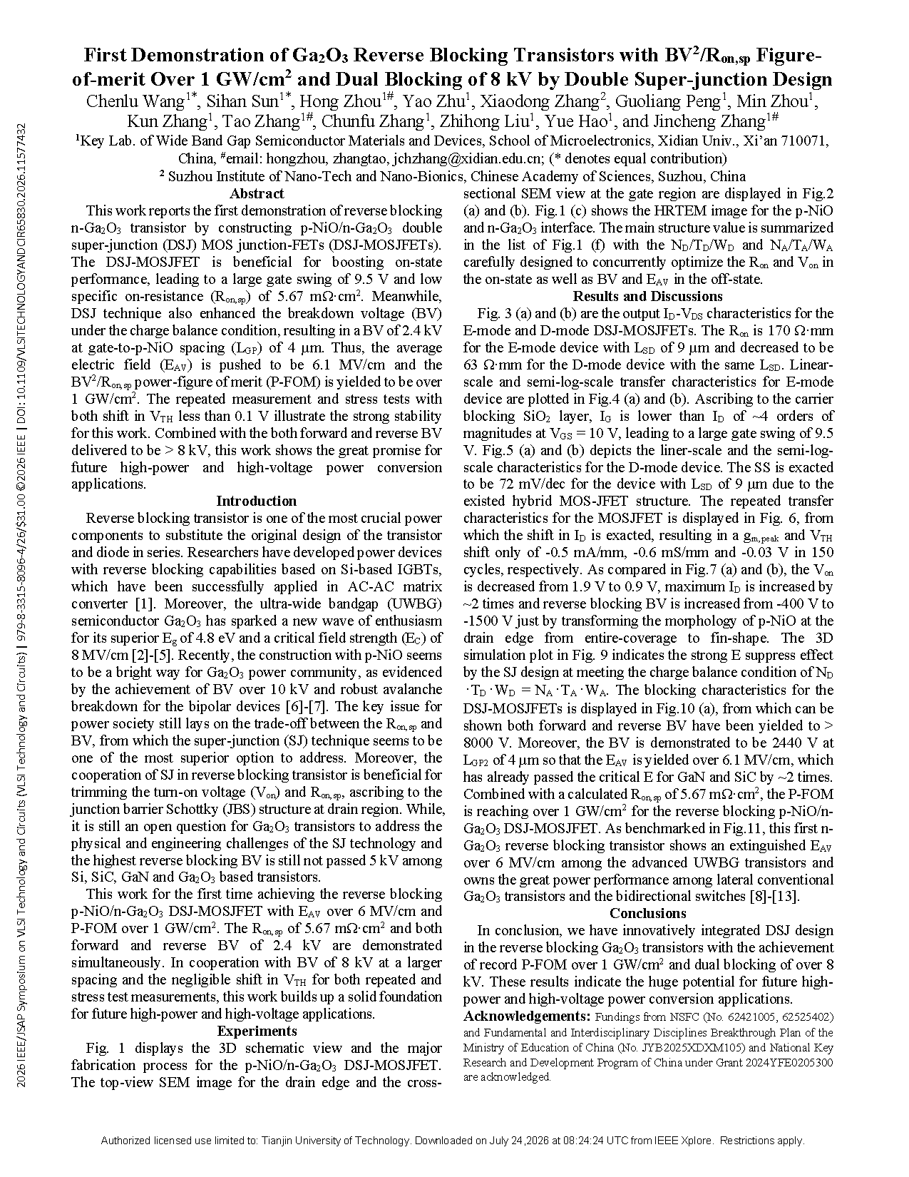
This work reports the first demonstration of reverse blocking n-Ga₂O₃ transistor by constructing p-NiO/n-Ga₂O₃ double super-junction (DSJ) MOS junction-FETs (DSJ-MOSJFETs). The DSJ-MOSJFET is beneficial for boosting on-state performance, leading to a large gate swing of 9.5 V and low specific on-resistance (Rₒₙ,ₛₚ) of 5.67 mΩ·cm². Meanwhile, DSJ technique also enhanced the breakdown voltage (BV) under the charge balance condition, resulting in a BV of 2.4 kV at gate-to-p-NiO spacing (LGP) of 4 μm. Thus, the average electric field (EAV) is pushed to be 6.1 MV/cm and the BV²/Rₒₙ,ₛₚ power-figure of merit (P-FOM) is yielded to be over 1 GW/cm². The repeated measurement and stress tests with both shift in VTH less than 0.1 V illustrate the strong stability for this work. Combined with the both forward and reverse BV delivered to be >8 kV, this work shows the great promise for future high-power and high-voltage power conversion applications.
Highlights
①First-ever fabrication of reverse blocking p-NiO/n-Ga₂O₃ DSJ-MOSJFET, breaking the limitation that reverse blocking voltage of existing Ga₂O₃ transistors is below 5 kV;
②Fin-shaped p-NiO drain-side super-junction alleviates channel depletion effect, reduces turn-on voltage Vₒₙ and specific on-resistance Rₒₙ,ₛₚ, and achieves a wide gate swing of 9.5 V with greatly improved on-state performance;
③Charge-balanced double super-junction realizes 3D uniform electric field modulation. At LGP=4 μm, forward/reverse BV reaches 2.4 kV with average electric field EAV=6.1 MV/cm, delivering a record power FOM over 1 GW/cm² (twice the critical electric field of GaN and SiC); bidirectional blocking voltage exceeds 8 kV with enlarged gate-drain spacing;
④Outstanding device stability verified by cycling and gate stress tests: VTH shift is only 0.03 V after 150 transfer cycles, and VTH drift is less than 0.1 V after 1000 s positive gate stress, proving high-quality gate oxide SiO₂ and p-NiO/n-Ga₂O₃ heterojunction interface.
Conclusion
In conclusion, we have innovatively integrated DSJ design in the reverse blocking Ga₂O₃ transistors with the achievement of record P-FOM over 1 GW/cm² and dual blocking of over 8 kV. These results indicate the huge potential for future high-power and high-voltage power conversion applications.
Project Support
This work was supported by the National Natural Science Foundation of China (Grant No. 62421005, 62525402), Fundamental and Interdisciplinary Disciplines Breakthrough Plan of the Ministry of Education of China (No. JYB2025XDXM105), and National Key Research and Development Program of China under Grant 2024YFE0205300.
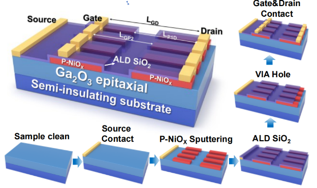
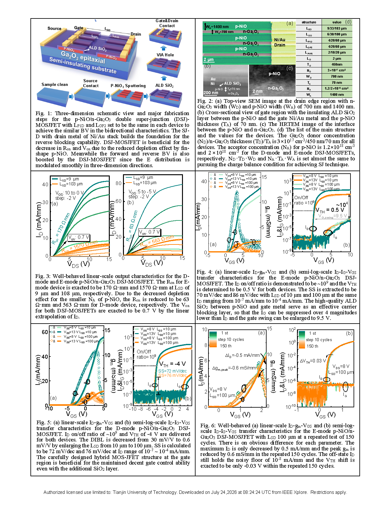
Fig. 1: Three-dimension schematic view and major fabrication steps for the p-NiO/n-Ga₂O₃ double super-junction (DSJ) MOSJFET with LP1D and LGP2 set to be the same in each device to achieve the similar BV in the bidirectional characteristics. The SJD with drain metal of Ni/Au stack builds the foundation for the reverse blocking capability. DSJ-MOSJFET is beneficial for the decrease in Rₒₙ and Vₒₙ due to the reduced depletion effect by finshape P-NiO. Meanwhile the forward and reverse BV is also boosted by the DSJ-MOSJFET since the E distribution is modulated smoothly in three-dimension directions.
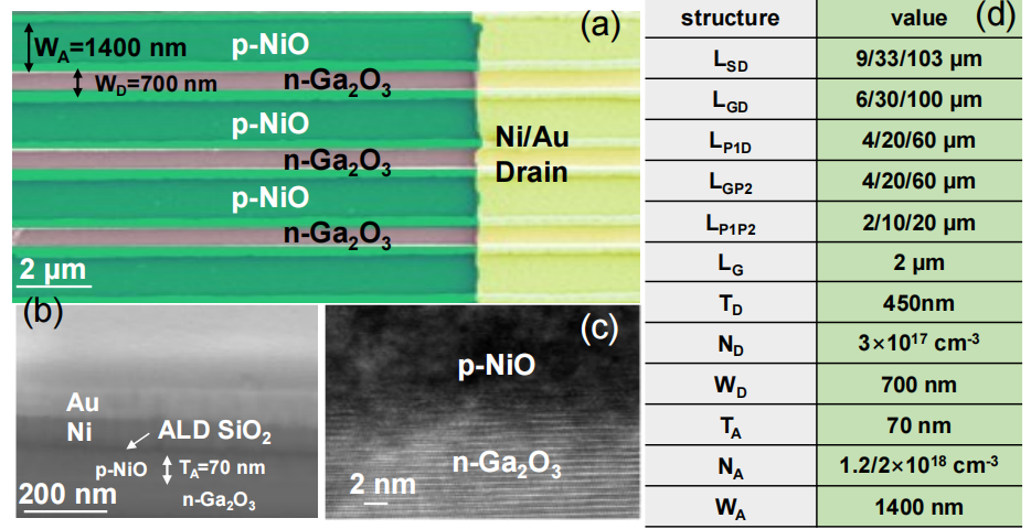
Fig. 2: (a) Top-view SEM image at the drain edge region with n-Ga₂O₃ width (WD) and P-NiO width (WA) of 700 nm and 1400 nm. (b) Cross-sectional view of gate region with the insulating ALD SiO₂ layer between the p-NiO and the gate Ni/Au metal and the p-NiO thickness (TA) of 70 nm. (c) The HRTEM image of the interface between the p-NiO and n-Ga₂O₃. (d) The list of the main structure and the values for the devices. The Ga₂O₃ donor concentration (ND)/n-Ga₂O₃ thickness (TD)/TA is 3×10¹⁷ cm⁻³/450 nm/70 nm for all devices. The acceptor concentration (NA) for p-NiO is 1.2×10¹⁸ cm⁻³ and 2×10¹⁸ cm⁻³ for the D-mode and E-mode DSJ-MOSJFETs, respectively. ND・TD・WD and NA・TA・WA is set almost the same to pursuing the charge balance condition for achieving SJ technique.
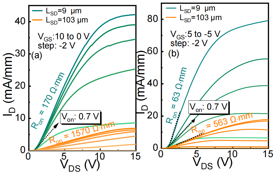
Fig. 3: Well-behaved linear-scale output characteristics for the D-mode and E-mode p-NiO/n-Ga₂O₃ DSJ-MOSJFET. The Rₒₙ for E-mode device is exacted to be 170 Ω・mm and 1570 Ω・mm at LSD of 9 μm and 108 μm, respectively. Due to the decreased depletion effect for the smaller NA of p-NiO, the Rₒₙ is reduced to be 63 Ω・mm and 563 Ω・mm for D-mode device, respectively. The Vₒₙ for both DSJ-MOSJFETs are exacted to be 0.7 V by the linear extrapolation of ID.
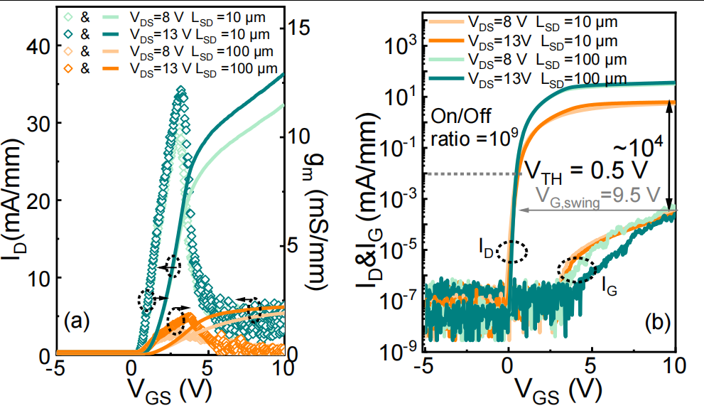
Fig. 4: (a) linear-scale ID-gm-Vgs and (b) semi-log-scale ID-Ig-VGs transfer characteristics for the E-mode p-NiO/n-Ga₂O₃ DSJ-MOSJFET. The ID on/off ratio is demonstrated to be ~109 and the VTH is determined to be 0.5 V for both devices. The SS is extracted to be 70 mV/dec and 86 mV/dec with Lsd of 10 um and 100 um at the same ID ranging from 10-7 mA/mm to 104 mA/mm. The high-quality ALD SiO2 between p-NiO and gate metal serve as an effective carrier blocking layer, so that the Ig can be suppressed over 4 magnitudes lower than ID and the gate swing can be enlarged to 9.5 V.
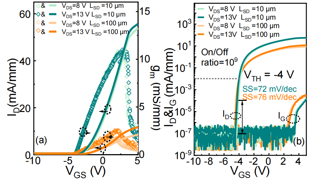
Fig. 5: (a) linear-scale ID-gₘ-VGS and (b) semi-log-scale ID-IG-VGS transfer characteristics for the D-mode p-NiO/n-Ga₂O₃ DSJ-MOSJFET. ID on/off ratio of ~10⁹ and VTH of -4 V are delivered for both devices. The DIBL is decreased from 30 mV/V to 0.6 mV/V by enlarging the LSD from 10 μm to 100 μm. SS is calculated to be 72 mV/dec and 76 mV/dec at ID range of 10⁻⁷ ~ 10⁻⁴ mA/mm. The carefully designed hybrid MOS-JFET structure at the gate region is beneficial for the maintained decent gate control ability even with the additional SiO₂ layer.
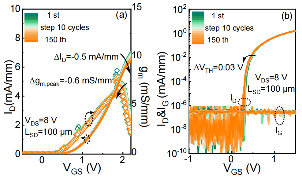
Fig. 6: Well-behaved (a) linear-scale ID-gₘ-VGS and (b) semi-logscale ID-IG-VGS transfer characteristics for the E-mode p-NiO/n-Ga₂O₃ DSJ-MOSJFET with LSD 100 μm at a repeated test of 150 cycles. There is no obvious difference for each parameter. The maximum ID is only decreased by 0.5 mA/mm and the peak gₘ is reduced by 0.6 mS/mm in the repeated 150 cycles. The off-state ID still holds the noisy floor of 10⁻⁸ mA/mm and the VTH shift is exacted to be only -0.03 V within the repeated 150 cycles.
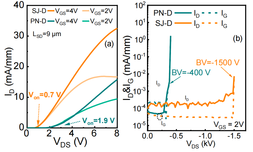
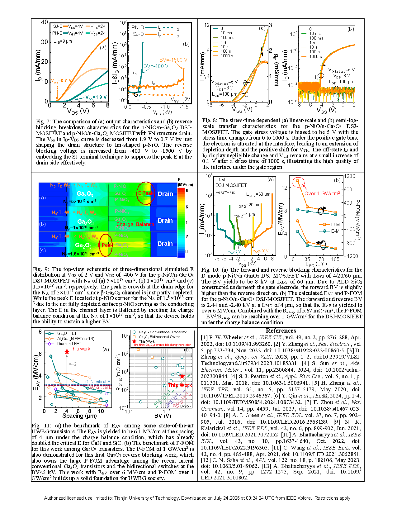
Fig. 7: The comparison of (a) output characteristics and (b) reverse blocking breakdown characteristics for the p-NiO/n-Ga₂O₃ DSJ-MOSJFET and p-NiO/n-Ga₂O₃ MOSJFET with PN structure drain. The Vₒₙ in ID-VDS curve is decreased from 1.9 V to 0.7 V by just shaping the drain structure to fin-shaped p-NiO. The reverse blocking voltage is increased from -400 V to -1500 V by embedding the SJ terminal technique to suppress the peak E at the drain side effectively.
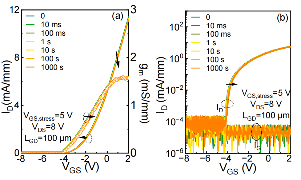
Fig. 8: The stress-time dependent (a) linear-scale and (b) semi-logscale transfer characteristics for the p-NiO/n-Ga₂O₃ DSJ-MOSJFET. The gate stress voltage is biased to be 5 V with the stress time changes from 0 to 1000 s. Under the positive gate bias, the electron is attracted at the interface, leading to an extension of depletion depth and the positive shift for VTH. The off-state ID and IG display negligible change and VTH remains at a small increase of 0.1 V after a stress time of 1000 s, illustrating the high quality of the interface under the gate region.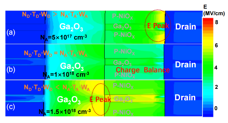
Fig. 9: The top-view schematic of three-dimensional simulated E distribution at VGS of 2 V and VDS of -400 V for the p-NiO/n-Ga₂O₃ DSJ-MOSJFET with NA of (a) 5×10¹⁷ cm⁻³, (b) 1×10¹⁸ cm⁻³ and (c) 1.5×10¹⁸ cm⁻³, respectively. The peak E crowds at the drain edge for the NA of 5×10¹⁷ cm⁻³ since β-Ga₂O₃ channel is just partly depleted. While the peak E located at p-NiO corner for the NA=1.5×10¹⁸ cm⁻³ due to the not fully depleted surface p-NiO serving as the conducting layer. The E in the channel layer is flattened by meeting the charge balance condition at the NA of 1×10¹⁸ cm⁻³, so that the device holds the ability to sustain a higher BV.
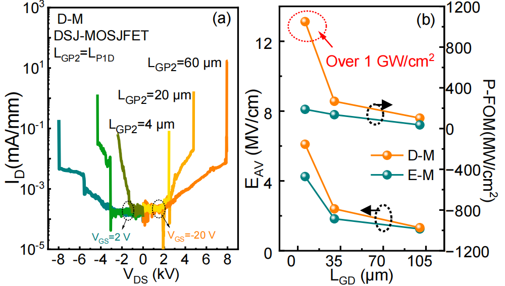
Fig. 10: (a) The forward and reverse blocking characteristics for the D-mode p-NiO/n-Ga₂O₃ DSJ-MOSJFET with LGP2 of 4/20/60 μm. The BV yields to be 8 kV at LGP2=60 μm. Due to ALD SiO₂ constructed underneath the gate electrode, the forward BV is slightly higher than the reverse direction. (b) The calculated EAV and P-FOM for the p-NiO/n-Ga₂O₃ DSJ-MOSJFET. The forward and reverse BV is 2.44 and -2.40 kV at a LP1D of 4 μm, so that the EAV is yielded to over 6 MV/cm. Combined with the Rₒₙ,ₛₚ 5.67 mΩ・cm², the P-FOM = BV²/Rₒₙ,ₛₚ can be reaching over 1 GW/cm² for the DSJ-MOSJFET under the charge balance condition.
DOI :
10.1109/VLSITechnologyandCir65830.2026.11577432
Instruction
Official Account

Cooperation
Top
