


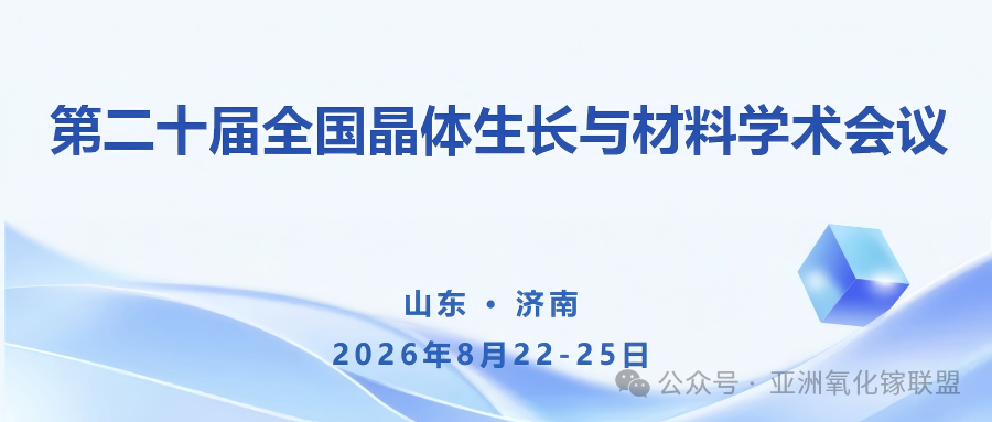
From August 22 to 25, the 20th National Conference on Crystal Growth and Materials (CCCG-20) will be held at the South Suburb Hotel in Jinan, Shandong Province. The conference focuses on crystal growth theory, semiconductor crystals, crystal growth technologies and equipment, and will concurrently host industry forums and equipment exhibitions. As a co-organizer of this conference, Garen Semiconductor will deeply engage in the conference exchanges, joining peers from across the industry to discuss technological innovation and industrial development.

During the conference, Professor Zhang Hui—jointly appointed by Zhejiang University and the Hangzhou International Science and Technology Innovation Center, and Chairman of Hangzhou Garen Semiconductor Co., Ltd.—will deliver an academic presentation titled "Progress and Challenges of Large-Size High-Quality Gallium Oxide Wafers" at the session on "Crystal Growth Technologies and Equipment." He will share relevant research progress with experts, scholars, and industry professionals, and jointly explore the opportunities and challenges in the development of large-size high-quality gallium oxide wafers.
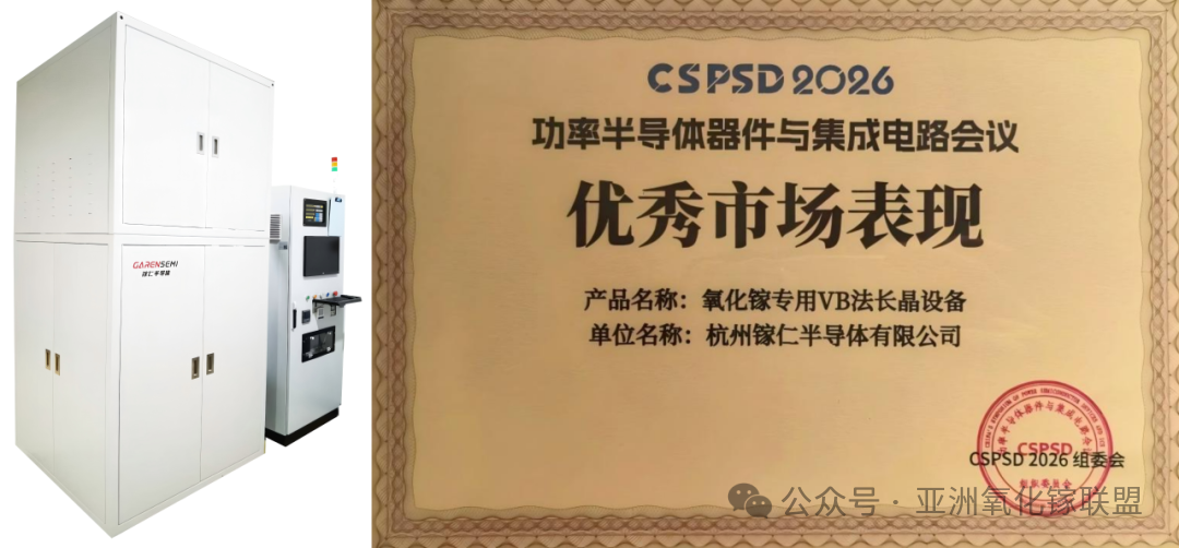
Crystal growth technologies and equipment represent a key focus area of this conference. Leveraging its deep expertise in gallium oxide crystal growth, Garen Semiconductor has independently developed a dedicated VB-method crystal growth equipment for gallium oxide. This equipment eliminates the need for frequent replacement of core components and flexibly accommodates the VB growth of 2- to 8-inch gallium oxide single crystals. It offers temperature control accuracy of ±0.1 °C with real-time data monitoring, and features a simple deployment process without requiring additional supply conditions such as process gases, compressed air, or cooling water. Additionally, the company provides a supporting growth process package, offering comprehensive support—from equipment to process—for universities, research institutes, and enterprises engaged in gallium oxide crystal growth research.
Recognized for its technological innovation and strong market performance, this equipment recently received the CSPSD 2026 Outstanding Market Performance Award, reflecting the market's recognition of the technical strength and application value of Garen Semiconductor's dedicated VB-method gallium oxide crystal growth equipment.
Garen Semiconductor sincerely invites you to join us in Jinan to exchange insights on technological advances and collectively shape the future of the industry.
About Garen Semiconductor
Hangzhou Garen Semiconductor Co., Ltd. is a global provider of gallium oxide materials and equipment solutions, specializing in the R&D and commercialization of ultra-wide-bandgap semiconductor technologies. The company’s core products include 2–8 inch gallium oxide single crystals and substrates (including the world’s first 8-inch products), vertical Bridgman (VB) gallium oxide crystal growth equipment, and 2–8 inch gallium oxide homoepitaxial wafers (including the world’s first 8-inch products). Garen Semiconductor is dedicated to building a fully integrated “equipment–crystal growth–substrate–epitaxy” industrial ecosystem and providing comprehensive solutions for global customers. The company’s achievements in gallium oxide have been widely recognized and featured by leading media outlets, including People’s Daily, Xinhua News Agency, Science and Technology Daily, Sina Finance, China Blue News, and The Paper.
For more information, please visit the official website: http://garen.cc/
Or contact us:
Mr. Jiang
Phone: +86 159 1871 9807
Email: jiangjiwei@garen.cc
Mr. Xia
Phone: +86 190 1127 8792
Email: xianing@garen.cc
Instruction
Official Account

Cooperation
Top
