


Recently, Fujia Gallium successfully grew a 6-inch Ga₂O₃ single-crystal ingot with a constant-diameter length exceeding 70 mm using its proprietary Vertical Bridgman (VB) method. High-resolution X-ray diffraction (HRXRD) characterization conducted by the Pinghu Laboratory confirmed excellent crystalline quality. Electrical characterization by the National Institute of Metrology (NIM), China, further demonstrated that the material meets the substrate requirements of the SiC industry.
Bulk Thickness Exceeds 70 mm, Further Highlighting Its Industrialization Potential
Ingot thickness is a key indicator of the maturity and industrialization of single-crystal growth technology. A thicker ingot allows more substrate wafers to be cut from a single crystal, directly reducing the cost per wafer.
The thickness of the 6-inch ingot was independently measured by the National Institute of Metrology (NIM), China, with an average thickness of 70.58 mm, exceeding the typical 20–50 mm thickness of mainstream SiC bulks.
HRXRD Multi-Point Measurements Confirm Excellent Crystal Quality
The Pinghu Laboratory conducted multi-point high-resolution X-ray diffraction (HRXRD) rocking-curve measurements on the VB-grown Ga₂O₃ substrate. The results are shown below:
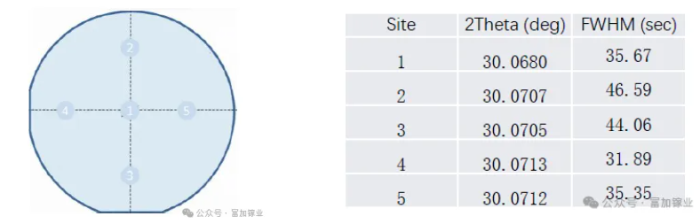
Multi-Point HRXRD Rocking-Curve Measurements of a 6-Inch VB-Grown Ga₂O₃ Substrate
The average FWHM across the five measurement points is 38.71 arcsec, with all five values below 50 arcsec, indicating excellent overall crystal quality and uniformity of the substrate.
Electrical Performance Verified by an Authoritative Third Party
Resistivity is a key parameter affecting the forward conduction performance of devices, while its uniformity is critical to device-to-device consistency and manufacturing yield. The National Institute of Metrology (NIM), China conducted electrical performance measurements on the 6-inch substrate, showing an average resistivity of 16.4 mΩ·cm and a uniformity of 6.8%.
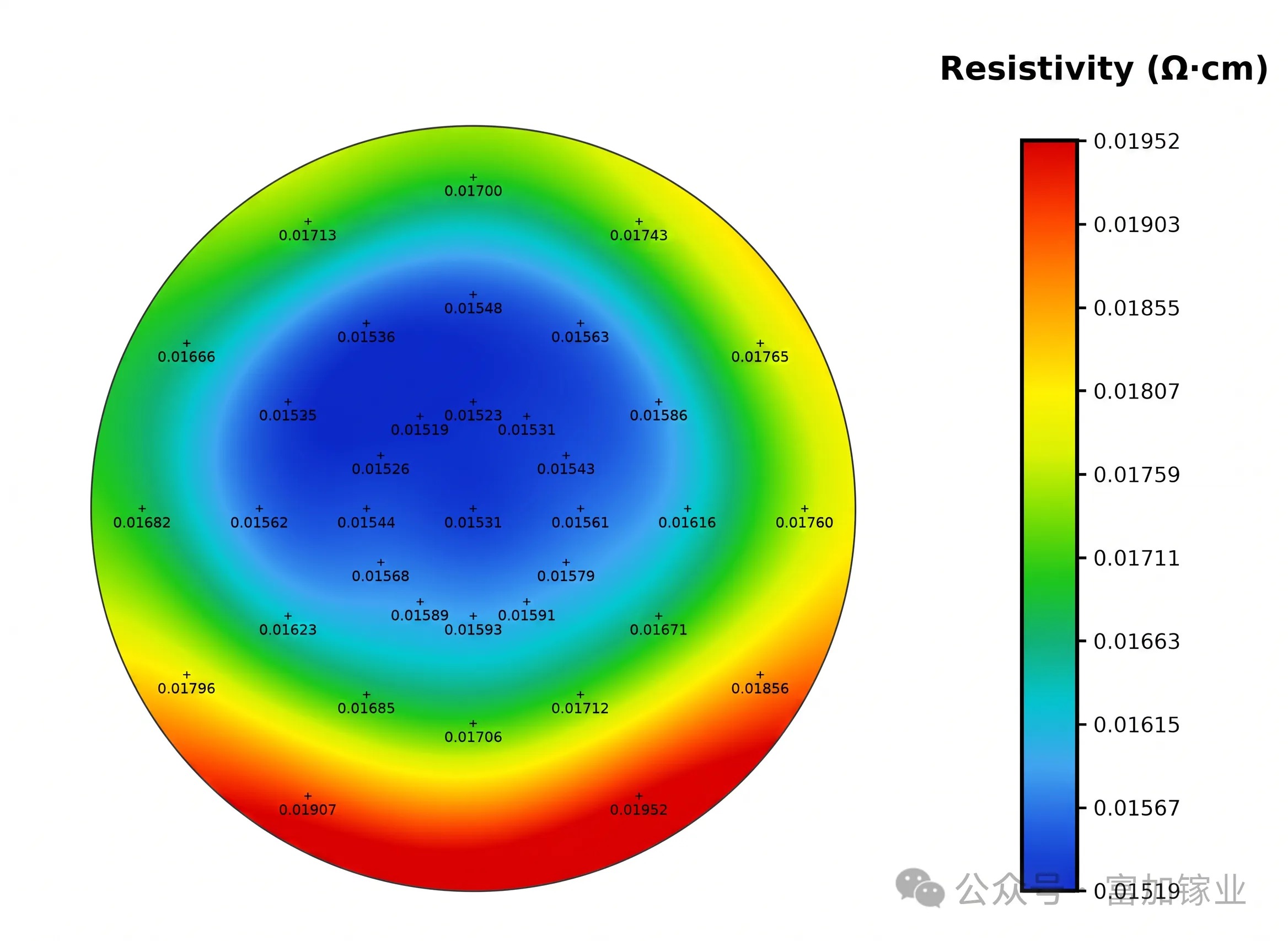
Electrical Performance Testing of a 6-Inch VB-Grown Ga₂O₃ Substrate
The test results indicate that the electrical performance meets the substrate requirements of the SiC industry.
Featured at the National Conference On Crystal Growth And Materials
It is worth noting that the 20th National Conference On Crystal Growth And Materials will be held from August 22 to 25, 2026, at the Nanjiao Hotel in Jinan, Shandong Province. Organized by the Crystal Growth and Materials Branch of the Chinese Ceramic Society and hosted by Shandong University, the conference will bring together experts and researchers in crystal growth and materials science.
Qi Hongji, a researcher at the Shanghai Institute of Optics and Fine Mechanics and Chairman of Fujia Gallium, will deliver a keynote presentation titled An Overview of the Industrialization Status of Gallium Oxide Single Crystals and Epitaxial Materials, sharing the latest progress in Ga₂O₃ industrialization.
During the conference exhibition, Fujia Gallium will also showcase a range of 2–8 inch Ga₂O₃ substrates and epitaxial products with different crystallographic orientations, including (100), (010), (001), and (011). Experts, researchers, and industry peers are welcome to visit the booth for discussion and exchange.
See you in Jinan, the City of Springs, for a gathering of the crystal-growth community.
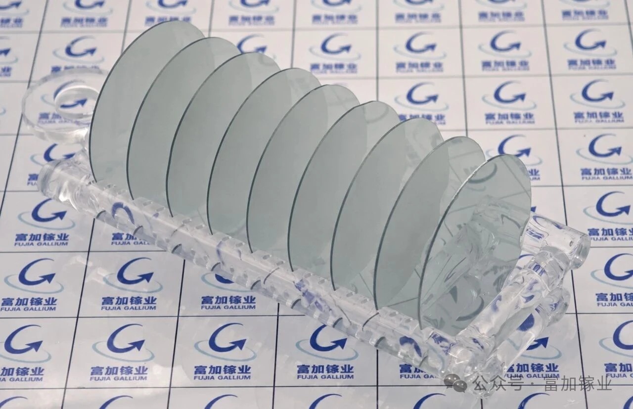
2-Inch Ga₂O₃ Substrate
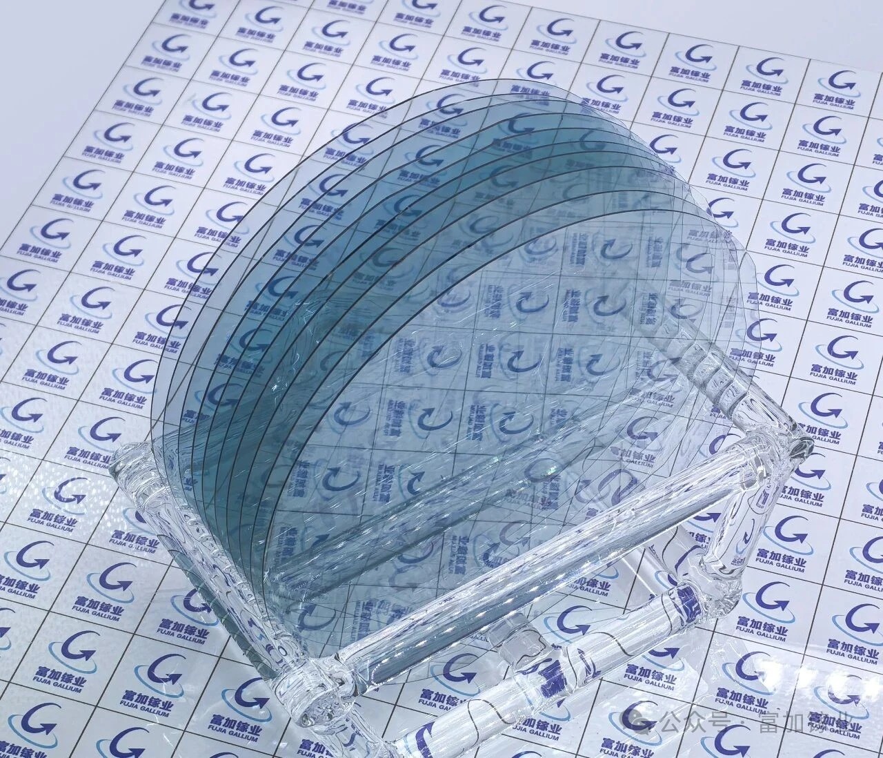
6-Inch Ga₂O₃ Substrate
From continuous breakthroughs in ingot thickness to comprehensive validation of crystal quality and electrical performance, Fujia Gallium is accelerating the industrialization of Ga₂O₃ materials, working to bring high-quality materials to customers worldwide.
Bringing Better Materials to the World — that’s what we’re working toward.
About Hangzhou Fujia Gallium
Hangzhou Fujia Gallium Technology Co., Ltd. was established on December 31, 2019. Guided by the vision of “Bringing Better Materials to the World,” the company is dedicated to the industrialization of ultra-wide-bandgap gallium oxide semiconductor materials. Its core products include gallium oxide single-crystal substrates, MOCVD/MBE epitaxial wafers, and crystal growth equipment based on the Vertical Bridgman (VB) and Edge-Defined Film-Fed Growth (EFG) methods. Recognized as a National High-Tech Enterprise, the company has undertaken multiple national and provincial/ministerial-level projects from the Ministry of Science and Technology, the National Development and Reform Commission, and the Ministry of Industry and Information Technology. It has been authorized nearly 65 international and domestic patents, and serves as the initiator and primary drafter of China's national standards in the field of gallium oxide. The company's series of major achievements in promoting gallium oxide industrialization have been featured in special coverages by prominent media outlets, including CCTV, People’s Daily, Xinhua News Agency, China Securities Journal, and The Paper.
Instruction
Official Account

Cooperation
Top
