


The development of a new product by Hangzhou Time-Tech Spectra has reached an important milestone. The SN-9000, the world’s first non-destructive dislocation inspection system for gallium oxide (Ga₂O₃) wafers, has officially been shipped and successfully delivered to a leading customer in the industry.
Designed to meet the dislocation-defect inspection needs of Ga₂O₃ substrates and epitaxial materials, the system provides critical inspection capabilities for Ga₂O₃ material research and development, quality control, and large-scale industrial production. The delivery marks a further breakthrough for Hangzhou Time-Tech Spectra in the field of materials inspection for fourth-generation semiconductors.

Key Equipment Highlights | SN-9000 Ga₂O₃ Wafer Non-Destructive Dislocation Inspection System
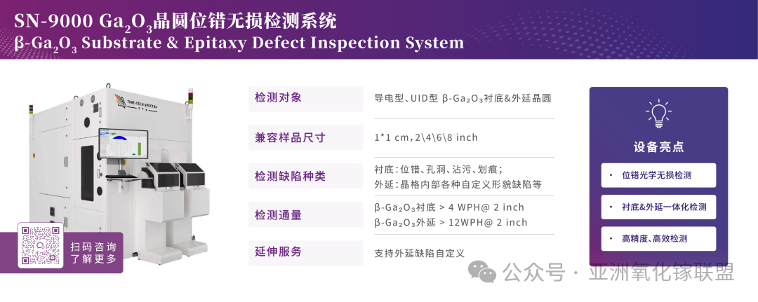
The SN-9000 from Hangzhou Time-Tech Spectra is built around two core advantages: non-destructive inspection and integrated testing. Combining high-speed, high-precision inspection, wide-size compatibility, and customizable defect analysis, the system provides a comprehensive inspection solution for β-Ga₂O₃ substrates and epitaxial materials, supporting applications from R&D and process development through mass production.
01 | Optical Non-Destructive Inspection for Wafer-by-Wafer and Batch Testing
The system employs optical non-destructive dislocation inspection technology, enabling precise identification of internal defects without damaging the sample. This not only ensures reliable inspection results but also avoids the loss of costly substrates and epitaxial wafers, making it particularly suitable for batch release and R&D validation of high-value β-Ga₂O₃ materials.
02 | Integrated Substrate and Epitaxial Wafer Inspection for One-Stop Quality Control
The system supports integrated inspection of both substrates and epitaxial wafers on a single platform, eliminating the need to switch between different inspection systems. This enables end-to-end quality monitoring from Ga₂O₃ substrates and epitaxial layers through epitaxial layers, significantly reducing handling time and the risk of cross-contamination while improving overall production-line efficiency.
03 | Precise Benchmarking Against XRT with Several-Fold Higher Inspection Efficiency
The SN-9000 delivers results that closely correlate with XRT measurements for detecting [010] dislocation lines in Ga₂O₃ substrates. Unlike XRT, which requires switching between multiple diffraction planes and performing separate scans to characterize dislocations in different orientations, the SN-9000 can identify dislocations with multiple orientations in a single inspection.
This enables several-fold higher inspection efficiency than XRT, while offering strong cost-effectiveness and a simplified operating workflow, making the system well suited for batch quality inspection and outgoing-product quality control on production lines.
04 | High Precision and High Throughput for Both Quality and Productivity
The SN-9000 can clearly distinguish dislocations, voids, contamination, and scratches, as well as various user-defined morphological defects within epitaxial layers.
For 2-inch wafers, the system achieves a throughput of more than 4 WPH for β-Ga₂O₃ substrate inspection and more than 12 WPH for epitaxial wafer inspection, delivering leading throughput at a comparable precision level and meeting the stringent speed requirements of high-volume production lines.
05 | Wide-Size Compatibility for Flexible Process Adaptation
The SN-9000 is compatible with 1 × 1 cm small samples and standard 2-, 4-, 6-, and 8-inch wafers, covering the full range of wafer sizes from R&D samples to large-scale production. Its multi-size compatibility enables a single system to serve multiple applications, helping reduce duplicate equipment investment.
06 | Customizable Epitaxial Defect Identification and Defect Traceability
The SN-9000 enables precise detection of various morphological defects in Ga₂O₃ epitaxial layers, with customizable defect-recognition capabilities to help manufacturers trace defect origins and continuously optimize epitaxial growth processes.
Leveraging its integrated substrate and epitaxial wafer inspection capability together with sub-micron-level positioning accuracy, the system can precisely correlate defect locations across the substrate and epitaxial layers. This makes it possible to directly observe how defects propagate from the substrate into the epitaxial layer, helping identify their underlying causes and providing actionable feedback for iterative improvements in Ga₂O₃ substrate preparation and epitaxial growth processes.

Scan the QR code to learn more about the equipment. We welcome inquiries and opportunities for collaboration.
Deepening Expertise to Empower the Upgrading of the Semiconductor Industry
As Ga₂O₃ materials continue to advance toward larger wafer sizes, high-volume manufacturing, and downstream device applications, the requirements for material defect inspection, quality assessment, and production process control are becoming increasingly stringent. The delivery of the Ga₂O₃ wafer non-destructive dislocation inspection system marks an important achievement for Hangzhou Time-Tech Spectra in continuously advancing product development and industrial applications to meet the inspection needs of fourth-generation semiconductor materials.
Looking ahead, Hangzhou Time-Tech Spectra will continue to address the inspection needs of compound semiconductor materials including SiC, GaN, Ga₂O₃, InP, and GaAs, while further developing an optical inspection product portfolio covering substrates, epitaxial layers, and devices. The company aims to further advance the non-destructive, automated, and data-driven capabilities of material defect inspection, providing robust technical support for the R&D and large-scale manufacturing of emerging semiconductor materials.
Instruction
Official Account

Cooperation
Top
