


From August 22 to 25, 2026, the 20th National Conference On Crystal Growth And Materials (CCCG-20) was held in Jinan. Hangzhou Fujia Gallium Technology Co., Ltd. showcased a number of high-profile products at the concurrent exhibition. The company disclosed for the first time detailed information on its breakthrough achievement of producing 6-inch gallium oxide ingots with an equal-diameter thickness exceeding 70 mm, and also exhibited 6-inch Ga₂O₃ substrate wafers in volume for the first time, drawing significant attention across the industry.
Ingot thickness is a key indicator of the maturity of single-crystal growth technology and its readiness for industrial-scale production. Using its proprietary vertical Bridgman (VB) method, Fujia Gallium has successfully grown 6-inch Ga₂O₃ single-crystal ingots with an equal-diameter thickness of more than 70 mm. At the exhibition, the company introduced 6-inch Ga₂O₃ substrate wafers in volume for the first time.
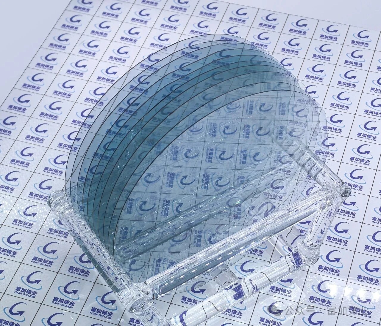
Figure 1. Fujia Gallium’s Batch of 6-Inch Ga₂O₃ Substrate Wafers
Multi-point HRXRD testing conducted by the Pinghu Laboratory in Shenzhen showed that the five measurement points on the substrate wafers had an average FWHM of only 38.71 arcsec, with all values below 50 arcsec. Electrical performance testing by the National Institute of Metrology (NIM), China, showed an average resistivity of 16.4 mΩ·cm, with a uniformity of 6.8%.
As early as October 2025, Fujia Gallium had already begun supplying 6-inch Ga₂O₃ substrate wafers. A thicker crystal ingot means more substrate wafers can be sliced from a single crystal, significantly reducing the cost per wafer. The concentrated exhibition of the ultra-thick ingots and batch-produced substrate wafers this time marks a steady improvement in the company’s capacity for volume production and supply.
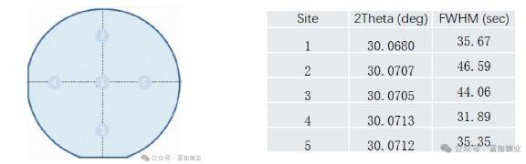
Figure 2. Multi-Point HRXRD Rocking-Curve Test Results of the 6-Inch Ga₂O₃ Substrate Wafers
The exhibition booth also showcased a range of 2- to 8-inch Ga₂O₃ substrate and epitaxial products with various crystal orientations, including (100), (010), (001), and (011).
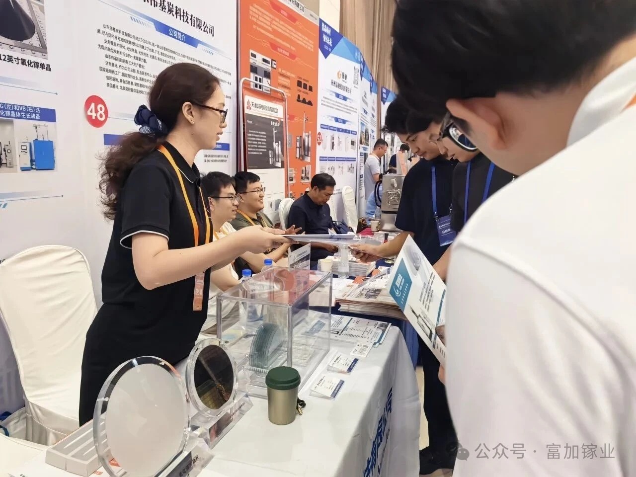
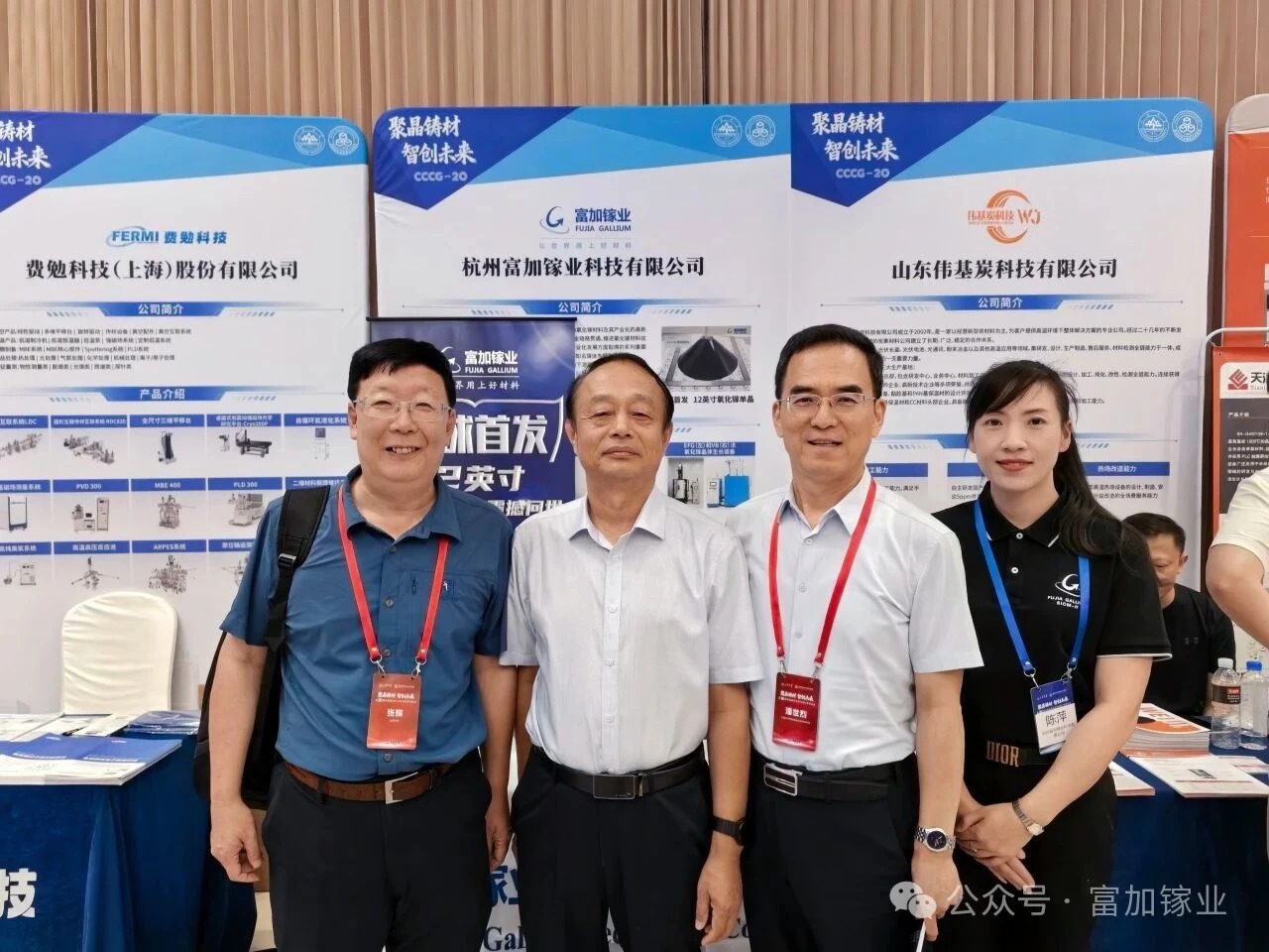
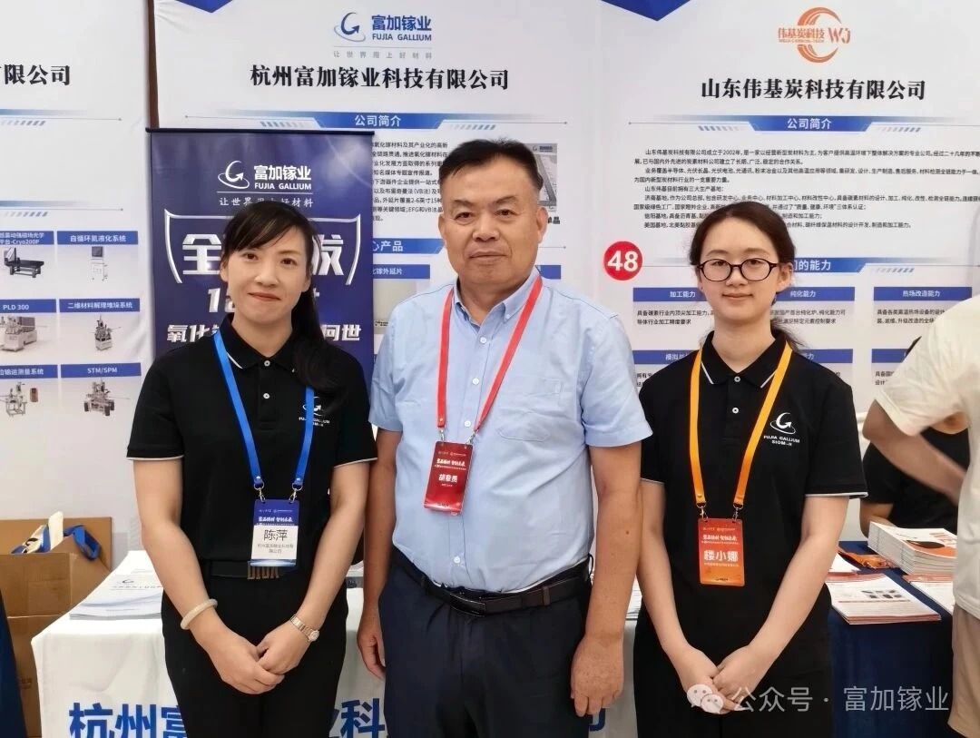
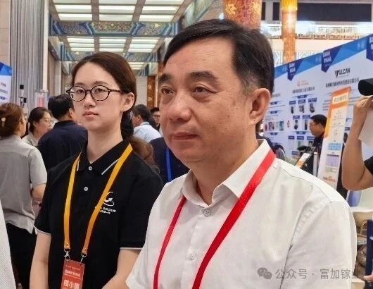
The booth attracted numerous academicians, experts, scholars, and industry professionals, who stopped by for discussions and exchanges. With its industry-leading ultra-thick crystal ingot technology and batch supply capability for 6-inch substrates, Fujia Gallium is continuing to strengthen its leading position in the industrialization of Ga₂O₃.
About Fujia Gallium
Hangzhou Fujia Gallium Technology Co., Ltd. was established on December 31, 2019. The company takes “Bringing Better Materials to the World” as its vision, and commits to the industrialization of ultra-wide bandgap semiconductor gallium oxide materials.
The company is a national high-tech enterprise, a Zhejiang Provincial specialized, refined, unique and innovative small and medium-sized enterprise, and a "quasi-unicorn" enterprise. It has undertaken many national and provincial-level projects from the Ministry of Science and Technology, National Development and Reform Commission, Ministry of Industry and Information Technology and other departments. It has obtained 65 authorized patents at home and abroad. It is the initiator and the first drafting unit of national standards in China’s gallium oxide industry. A series of important achievements achieved by the company in promoting gallium oxide industrialization have been reported and publicized by well-known media such as CCTV, People’s Daily, Xinhuanet, Science and Technology Daily, China Securities Journal and The Paper.
Instruction
Official Account

Cooperation
Top
