


Shanghai’s 15th Five-Year Plan for Integrated Circuits: Advanced Manufacturing, Compound Semiconductors and Key Equipment in Focus
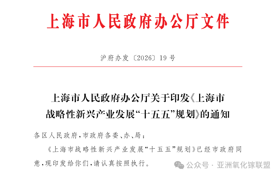
Recently, the General Office of the Shanghai Municipal People’s Government issued the 14th Five-Year Plan for the Development of Shanghai’s Strategic Emerging Industries, which identifies fourth-generation semiconductors as a key area for future frontier technology development. The plan calls for advancing R&D on ultra-wide-bandgap semiconductor technologies, including gallium oxide, diamond, and aluminum nitride, while accelerating their applications in power electronics, radio frequency, sensing, and other fields.
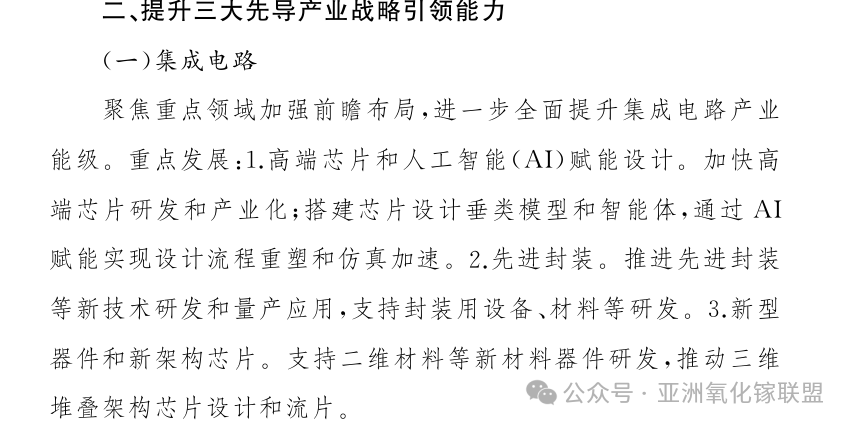
In terms of industrial positioning, Shanghai has identified integrated circuits as one of its three leading industries. During the 15th Five-Year Plan period, the city will further enhance the overall competitiveness of its integrated circuit industry, with a focus on high-end chip and AI-enabled design, advanced packaging, novel devices, and new chip architectures. The plan also calls for supporting the development of new-material devices, including those based on two-dimensional materials, and promoting the design and tape-out of chips featuring three-dimensional stacking architectures.
In the field of fourth-generation semiconductors, the plan outlines a relatively clear technological roadmap. On the one hand, it prioritizes ultra-wide-bandgap materials such as gallium oxide, diamond, and aluminum nitride; on the other, it also highlights ultra-narrow-bandgap materials such as antimonides. The focus extends beyond materials research to target application scenarios including power electronics, radio frequency, and sensing.

From the perspective of industrialization, the plan calls for advancing the R&D, commercialization, and mass production of emerging technologies such as advanced packaging, while supporting the development of packaging equipment and materials to further strengthen the industrialization capabilities and key supporting infrastructure of the integrated circuit sector.
Shanghai is also not pursuing fourth-generation semiconductors as an isolated initiative. Instead, the city is integrating them into a broader future technology ecosystem encompassing integrated circuits, novel devices, artificial intelligence, optical computing, and 6G. The plan also identifies frontier areas such as optical computing chips and 6G, providing potential application drivers for emerging semiconductor materials and devices.
In terms of industrial geography, Shanghai has established a multi-node integrated circuit industry layout. Zhangjiang Science City will focus on enhancing the capabilities of its integrated circuit industrial cluster, while the Lingang Special Area will cultivate and expand hard-tech industries including integrated circuits and civil aviation. Jiading will focus on integrated circuits and intelligent sensors, while Xuhui’s Caohejing area will continue to strengthen its integrated circuit design capabilities. Zhangjiang will also support innovation and development in future industries such as quantum technology and optical computing.
From the perspective of the overall targets, by 2030, Shanghai aims to increase the added value of its strategic emerging industries to RMB 2.1 trillion, with the total output value of strategic emerging industries in the industrial sector accounting for more than 50% of the total output value of industries above designated size. During the 15th Five-Year Plan period, the annual average growth rate of the manufacturing sector in the three leading industries is targeted to exceed 10%.
For the semiconductor industry, the key signal from the plan is that Shanghai has moved gallium oxide beyond standalone materials research and incorporated it into the broader future-industry framework for fourth-generation semiconductors, with a clear focus on extending the technology toward device applications in power electronics, RF, and sensing. Meanwhile, leveraging Shanghai’s mature integrated circuit industry chain and industrial clusters in Zhangjiang, Lingang, and Jiading, the potential for collaboration between fourth-generation semiconductors and traditional integrated circuits, novel semiconductor devices, and artificial intelligence is further expanding.
Fujian’s 15th Five-Year Plan Steps Up Investment in Semiconductor Materials: SiC and GaN Target Commercialization, While Ga₂O₃, Diamond and AlN Enter the Strategic Pipeline
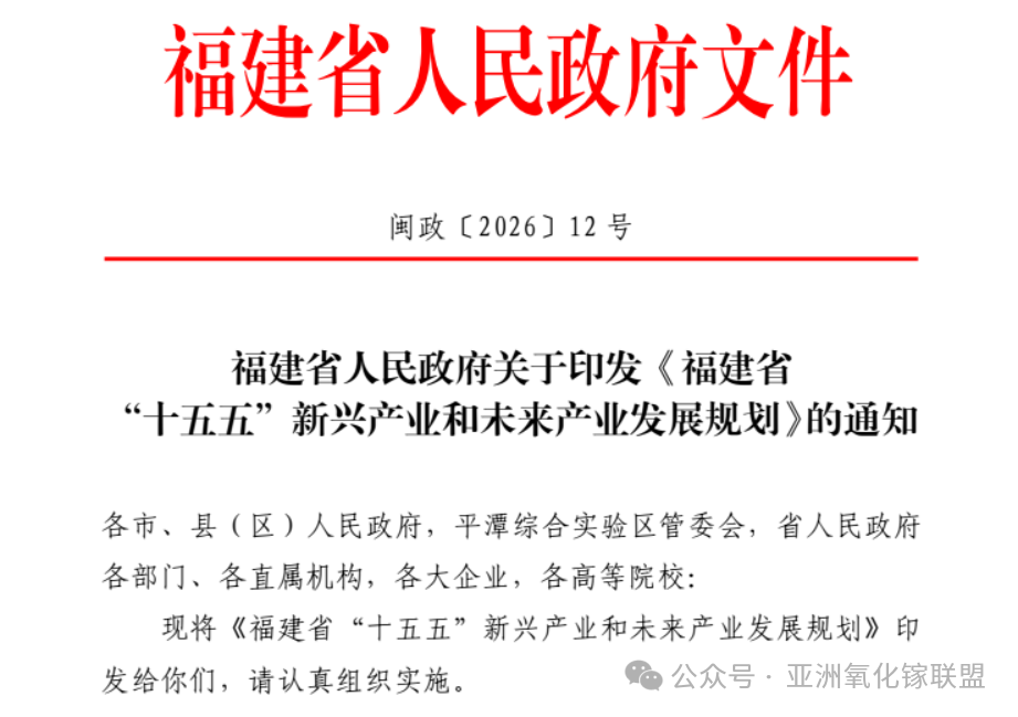
Recently, the Fujian Province 15th Five-Year Plan for the Development of Emerging and Future Industries was released. The plan proposes establishing a “369” system for emerging and future industries, identifying new energy, new materials, integrated circuits, and optoelectronics as key emerging industries. It also identifies compound semiconductors as a priority track within the integrated circuit and optoelectronics sectors.
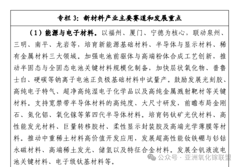
Notably, gallium oxide (Ga₂O₃) is explicitly included in Fujian’s development plans for fourth-generation semiconductor materials. In the field of energy and electronic materials, the plan calls for supporting the development of wide-bandgap semiconductor materials toward higher purity and larger wafer sizes in response to the needs of the new energy and semiconductor industries, while making forward-looking investments in fourth-generation semiconductor materials such as diamond, aluminum nitride (AlN), and gallium oxide.
Fujian’s strategy for ultra-wide-bandgap semiconductors extends beyond the materials side. Within the integrated circuit and optoelectronics industries, the plan explicitly calls for developing compound semiconductors, advancing wide-bandgap and ultra-wide-bandgap semiconductor technologies, and accelerating the development of a full-chain industrial ecosystem.
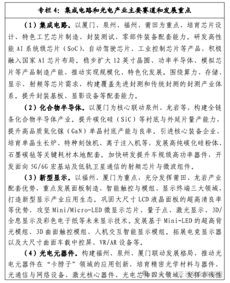
In terms of industrial chain development, Fujian plans to build a compound semiconductor industry system centered on Xiamen, with coordinated development across Quanzhou and Longyan. The plan calls for increasing the mass-production capacity of silicon carbide (SiC) substrates and epitaxial wafers, while expanding the capacity and improving the yield of high-quality gallium nitride (GaN) single-crystal substrates. It also proposes attracting key equipment companies, cultivating equipment such as single-crystal growth furnaces, specialized etching machines, and ion implanters, and developing local supply capabilities for key consumables including high-purity SiC powders and graphite carbon felts.
On the device side, Fujian will focus on the R&D of automotive-grade high-power devices, while developing RF chips and microwave components for 5G/6G macro base stations and low-Earth-orbit satellite communications. This indicates that Fujian’s strategy for wide-bandgap and ultra-wide-bandgap semiconductors is not limited to materials R&D, but extends across the entire value chain from substrates and epitaxy to equipment, consumables, devices, and applications.
In terms of industrial targets, by 2030, Fujian aims to grow its new materials industrial cluster to more than RMB 900 billion and its integrated circuit and optoelectronics industrial clusters to more than RMB 300 billion. The province also aims for the output value of strategic emerging industries in the industrial sector to account for approximately 35% of the total industrial output value of enterprises above designated size.
For the gallium oxide industry, the key signal from the plan is that Fujian has explicitly incorporated gallium oxide into its fourth-generation semiconductor materials strategy and placed it within a broader industrial framework for wide-bandgap and ultra-wide-bandgap semiconductors. Although the plan does not yet specify separate development pathways for Ga₂O₃ substrates, epitaxy, or devices, its emphasis on high-purity, large-size materials and the development of a full-chain compound semiconductor ecosystem provides clear policy entry points and industrial space for the future development of the Ga₂O₃ industry.
Instruction
Official Account

Cooperation
Top
