


Researchers from the Xidian University and Chinese Academy of Sciences have published a dissertation titled " Annealing-Driven Strain-Relaxation Transition and Its Direct Impact on Transport in Heteroepitaxial β-Ga₂O₃ MOSFETs " in IEEE Transactions on Electron Devices.
Background
Gallium oxide β-Ga₂O₃, an ultra-wide bandgap semiconductor with ultrahigh breakdown electric field, is a promising candidate material for next-generation high-power electronic devices. At present, homoepitaxial β-Ga₂O₃-based diodes and MOSFETs have achieved outstanding electrical performance, while the native single-crystal β-Ga₂O₃ substrates suffer from extremely high manufacturing cost and great difficulty in large-size wafer mass production, which restrict their industrial large-scale application.
Sapphire substrates feature low cost and availability of large-size wafers, with a bandgap of ~8.8 eV and thermal conductivity of ~40 W·m⁻¹·K⁻¹, exhibiting favorable thermal matching with β-Ga₂O₃. Therefore, sapphire serves as the most industrially valuable substrate for heteroepitaxial β-Ga₂O₃. Nevertheless, severe lattice and thermal expansion mismatch exists between β-Ga₂O₃ and sapphire. After heteroepitaxial growth, the thin films generate massive rotational domains, dislocations, oxygen vacancies Vo,gallium vacancies VGa and other defects. These defects strongly scatter carriers, degrade the on-state current, ION/IOFF ratio, breakdown voltage and high-temperature stability of devices, forming the core performance bottleneck of sapphire-based β-Ga₂O₃ power devices.
High-temperature post-annealing is a critical process to regulate the microstructure, defect concentration and interfacial strain of heteroepitaxial thin films. Existing studies only explore the influence of growth temperature on film domain structures, or separately analyze Al diffusion and defect evolution after annealing. The strain-relaxation transition mechanism at heterointerface induced by annealing has not been systematically established, and the direct correlation among “microscopic lattice-defect evolution-device transport properties” is missing. High-temperature annealing brings two competing effects: the beneficial effect including strain homogenization and defect healing, and the detrimental effect that interdiffusion of Al elements from substrate triggers localized strain accumulation and newly generated scattering defects. It remains unclear how annealing temperature forms a critical transition window balancing the two effects, the evolution rules of interfacial dislocations, shear strain and vacancy defects under different annealing temperatures, as well as the quantitative impact of such microscopic changes on MOSFET electrical characteristics and high-temperature reliability. No complete and systematic research has been reported, failing to provide standardized thermal budget guidelines for low-cost sapphire-based high-performance β-Ga₂O₃ devices.
Abstract
This work correlates the annealing-driven strain relaxation with its decisive impact on carrier transport in heteroepitaxial β-Ga₂O₃/sapphire MOSFETs. High-resolution transmission electron microscopy (HRTEM), fast Fourier transform (FFT), and geometric phase analysis (GPA) reveal that substrate clamping leads to rotational domains and dislocations, which limit transport at 800 ◦C–900 ◦C. At a critical transition temperature of 1000 ◦C, the strain field is homogenized, substrate clamping is suppressed, and gallium vacancies are reduced. Conversely, 1100 ◦C annealing triggers Al interdiffusion and reintroduces localized strain accumulation that degrades lattice quality. Consequently, MOSFETs on 1000 ◦C-annealed films exhibit a 14-fold saturation current enhancement, a 100-fold ION/IOFF ratio improvement, and a 1050-V breakdown voltage. The optimized devices also demonstrate excellent operational stability at 200 ◦C, with thermal stability comparable to homoepitaxial counterparts. By identifying the window between “defect-healing” and “damage-inducing” regimes, this study provides critical thermal budget guidelines for high-performance β-Ga₂O₃ power electronics.
Highlights
Combined multi-scale characterizations including HRTEM, FFT, GPA strain mapping, XRD, XPS, PL and EDS systematically uncover the full annealing-driven strain-relaxation transition at heterointerface of heteroepitaxial β-Ga₂O₃/sapphire thin films for the first time, and clarify three-stage microstructural evolution rule from 800 ℃ to 1100 ℃: substrate clamping generates rotational domains and high-density dislocations at 800–900 ℃; 1000 ℃ acts as the critical transition temperature with homogenized strain field and suppressed gallium vacancies; annealing at 1100 ℃ triggers Al interdiffusion from sapphire and reintroduces localized strain accumulation, deteriorating lattice quality.
Direct quantitative correlation between annealing temperature, lattice strain/defect evolution and carrier transport performance of β-Ga₂O₃ MOSFETs is established, and 1000 ℃ is confirmed as the optimal thermal budget window balancing defect healing and interfacial stability. Quantitative performance improvements are achieved on devices with 1000 ℃-annealed films: 14× higher saturation drain current, 100× enhanced ION/IOFFratio and 1050 V breakdown voltage.
Two competing annealing mechanisms are clarified: low-temperature annealing is dominated by carrier scattering induced by massive defects; 1000 ℃ annealing brings beneficial defect elimination and strain homogenization; temperature above 1100 ℃ causes irreversible device damage originating from Al interdiffusion. XPS and PL characterizations verify the minimum oxygen vacancy concentration, maximum lattice oxygen proportion and optimal activation efficiency of Si dopant under 1000 ℃ post-annealing.
MOSFETs fabricated on 1000 ℃-annealed β-Ga₂O₃ films exhibit outstanding thermal stability up to 200 ℃ with a stable specific on-resistance of 0.3 Ω·cm², whose high-temperature reliability is comparable to homoepitaxial β-Ga₂O₃ counterparts. This work delivers explicit thermal processing guidelines for industrialized low-cost sapphire-based high-power β-Ga₂O₃ electronic devices.
Conclusion
This work establishes a direct correlation between annealing-driven strain-relaxation transition and carrier transport in heteroepitaxial β-Ga₂O₃/sapphire MOSFETs. Multiscale characterization reveals pronounced structural evolution at the heterointerface. At 800 ◦C–900 ◦C, strong substrate clamping generates high-density dislocations and rotational misorientation domains that limit device transport. At the optimal temperature of 1000 ◦C, transition to a homogenized strain state effectively promotes dopant activation and suppresses charged vacancy scattering, yielding superior gate controllability, significantly reduced C–V frequency dispersion, and enhanced current drive capability. Conversely, annealing at 1100 ◦C initiates diffusion-assisted strain relaxation, where Al interdiffusion reintroduces compositional inhomogeneity and localized shear stress that degrade channel transport. The optimized MOSFETs achieve a Vbr of 1050 V and an ION/IOFF ratio two orders of magnitude higher than those of 800 ◦C devices. Furthermore, the stable transfer characteristics up to 200 ◦C demonstrate forward-bias thermal stability comparable to state-of-the-art homoepitaxial devices. These findings highlight that precisely controlling the strain-relaxation pathway to balance defect healing and interfacial stability is critical for realizing high-performance heteroepitaxial β-Ga₂O₃ power devices.
Project Support
This work was supported in part by the Key Program of Shaanxi Provincial Department of Science and Technology Support under Grant 2024CY2-GJHX-81 and in part by the National Natural Science Foundation of China under Grant 62293522.
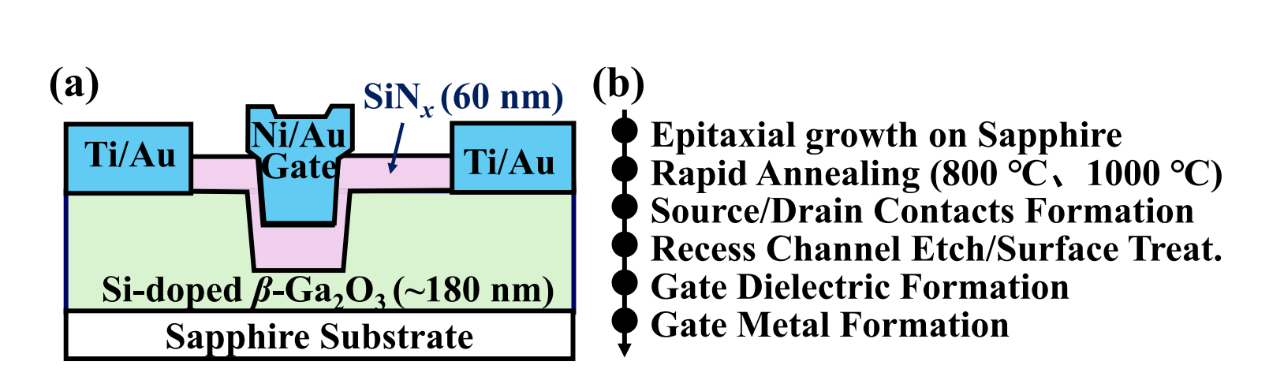
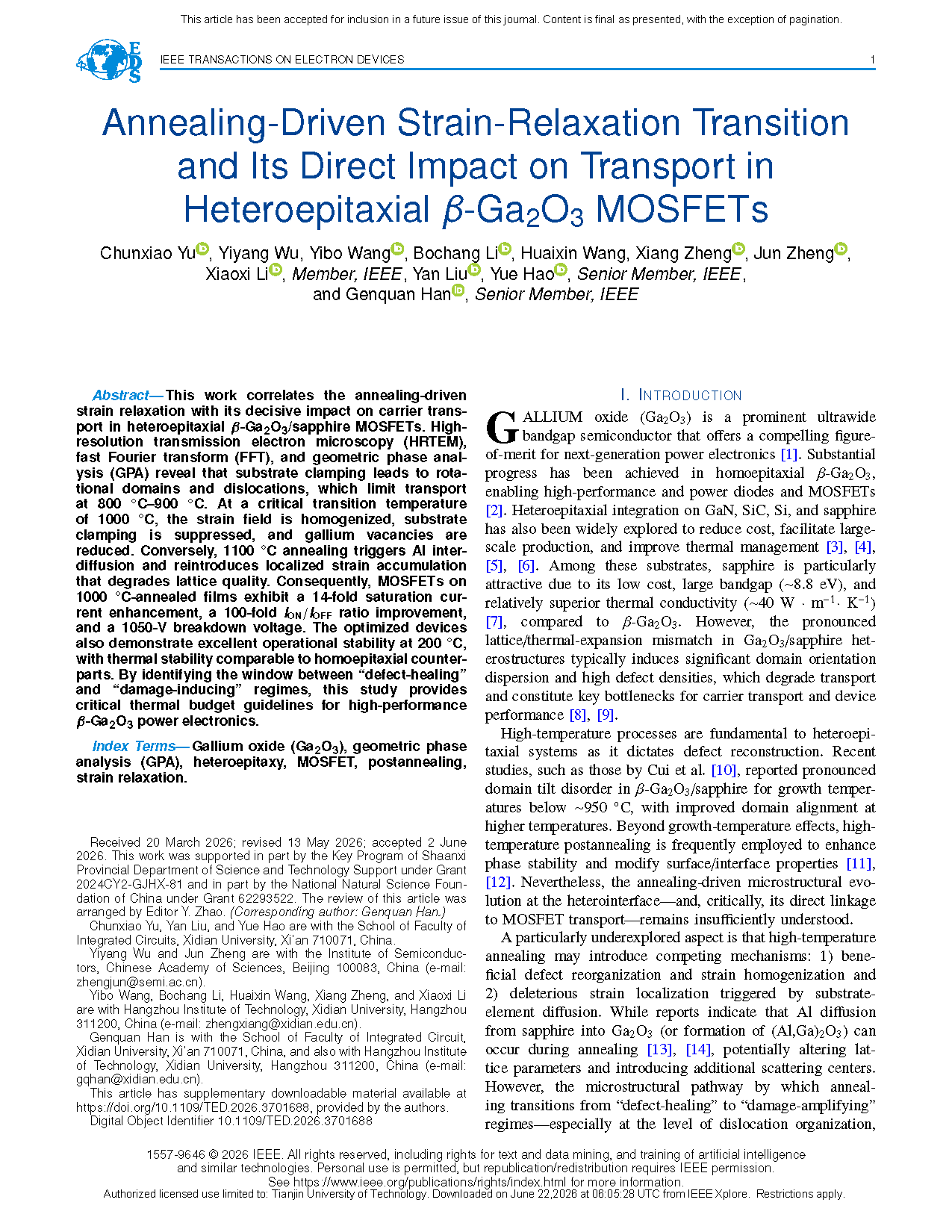
Fig. 1. (a) Schematic cross section of the fabricated recessed-gate β-Ga₂O₃/sapphire MOSFET. (b) Summary of the device fabrication process flow.
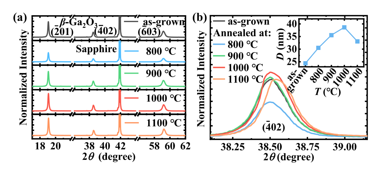
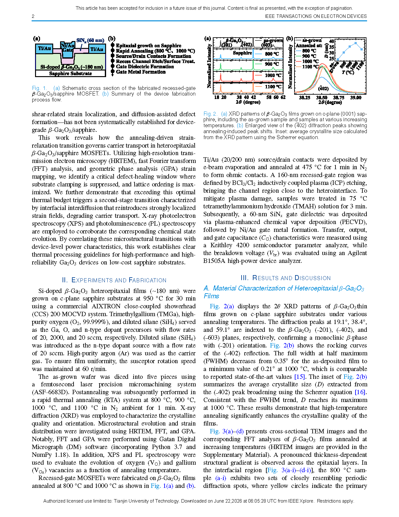
Fig. 2. (a) XRD patterns of β-Ga₂O₃ films grown on c-plane (0001) sapphire, including the as-grown sample and samples at various increasing annealing-induced peak shifts. Inset: average crystallite size calculated from the XRD pattern using the Scherrer equation.
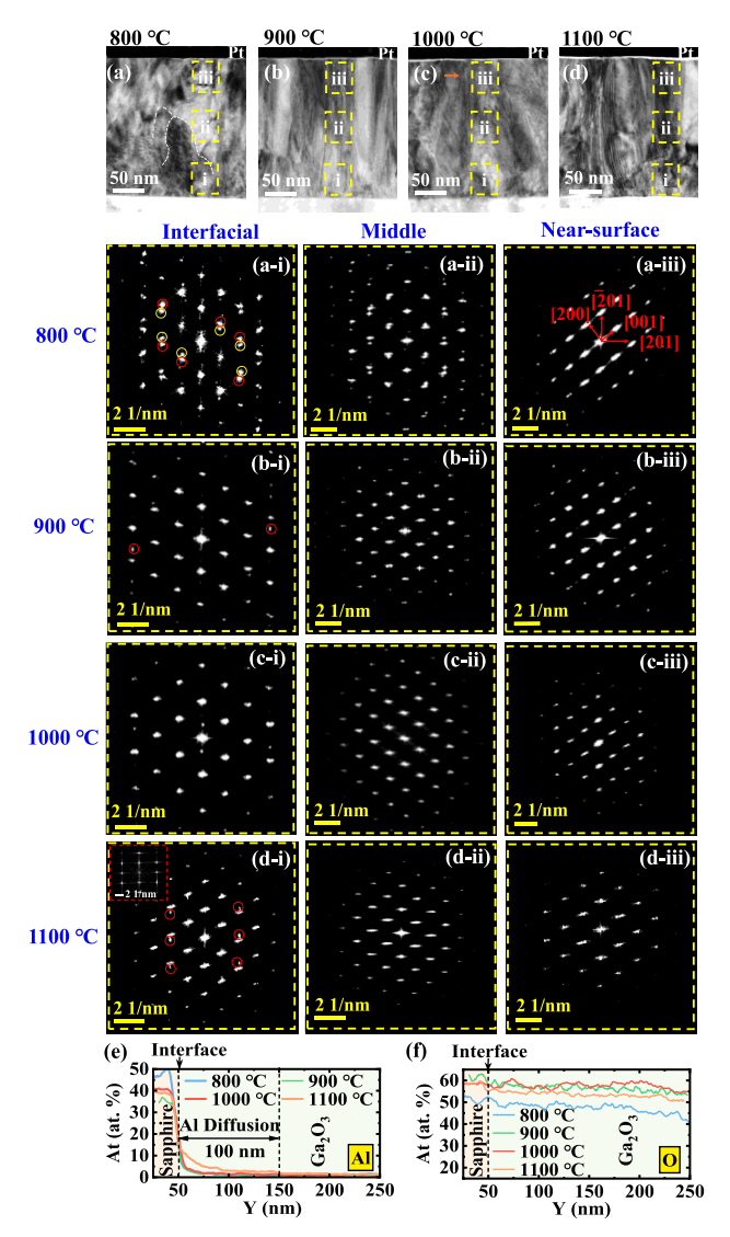
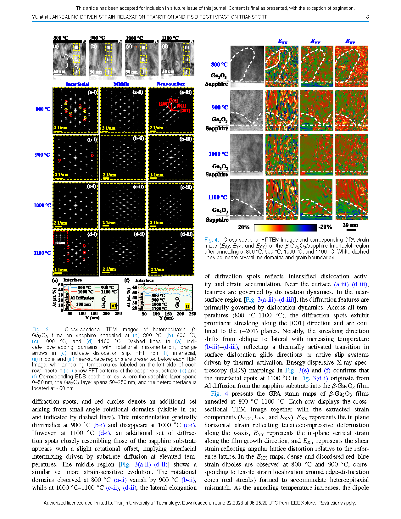
Fig. 3. Cross-sectional TEM images of heteroepitaxial Ga₂O₃ films on sapphire annealed at (a) 800 ◦C, (b) 900 ◦C, (c) 1000 ◦C, and (d) 1100 ◦C. Dashed lines in (a) indicate overlapping domains with rotational misorientation; orange arrows in (c) indicate dislocation slip. FFT from (i) interfacial, (ii) middle, and (iii) near-surface regions are presented below each TEM image, with annealing temperatures labeled on the left side of each row. Insets in (d-i) show FFT patterns of the sapphire substrate. (e) and (f) Corresponding EDS depth profiles, where the sapphire layer spans 0–50 nm, the Ga₂O₃ layer spans 50–250 nm, and the heterointerface is located at ∼50 nm.
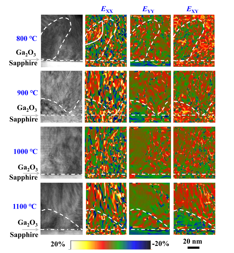
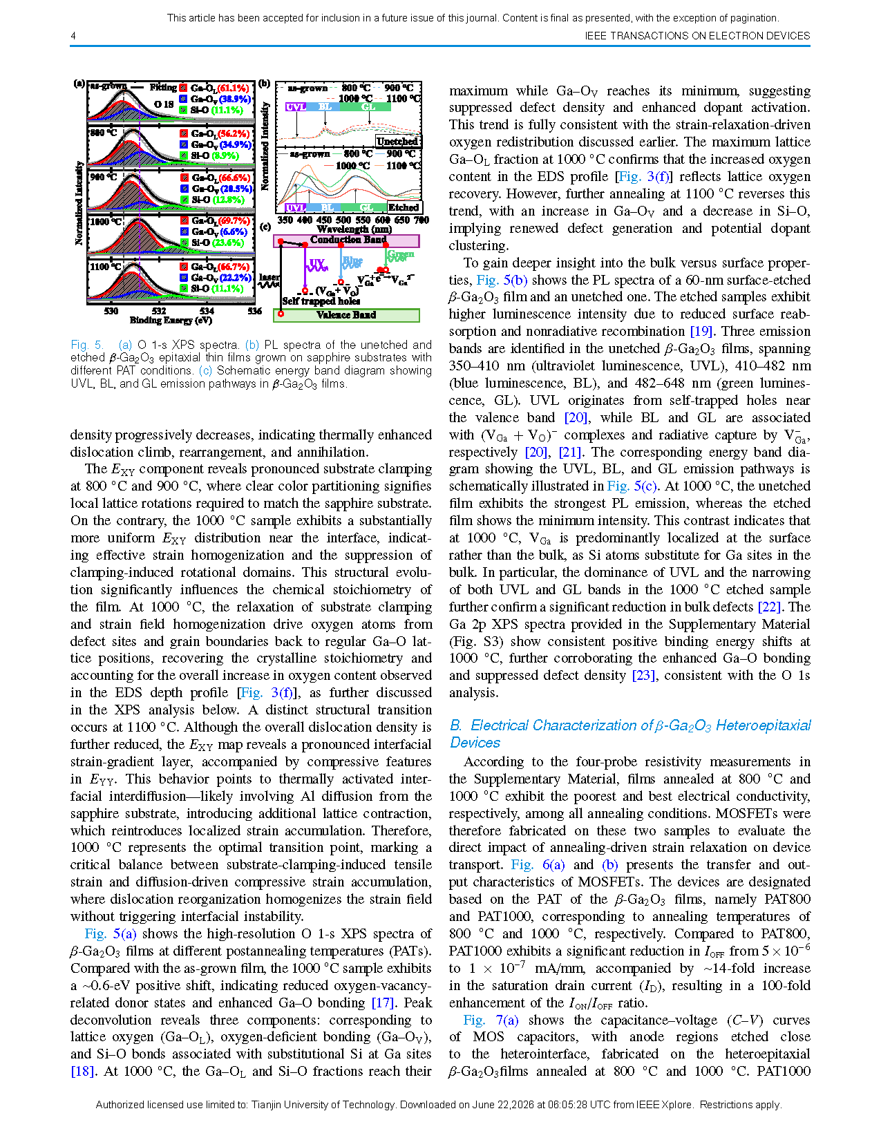
Fig. 4. Cross-sectional HRTEM images and corresponding GPA strain maps (EXX, EYY, EXY) of the β-Ga₂O₃/sapphire interfacial region after annealing at 800 ◦C, 900 ◦C, 1000 ◦C, and 1100 ◦C. White dashed lines delineate crystalline domains and grain boundaries.
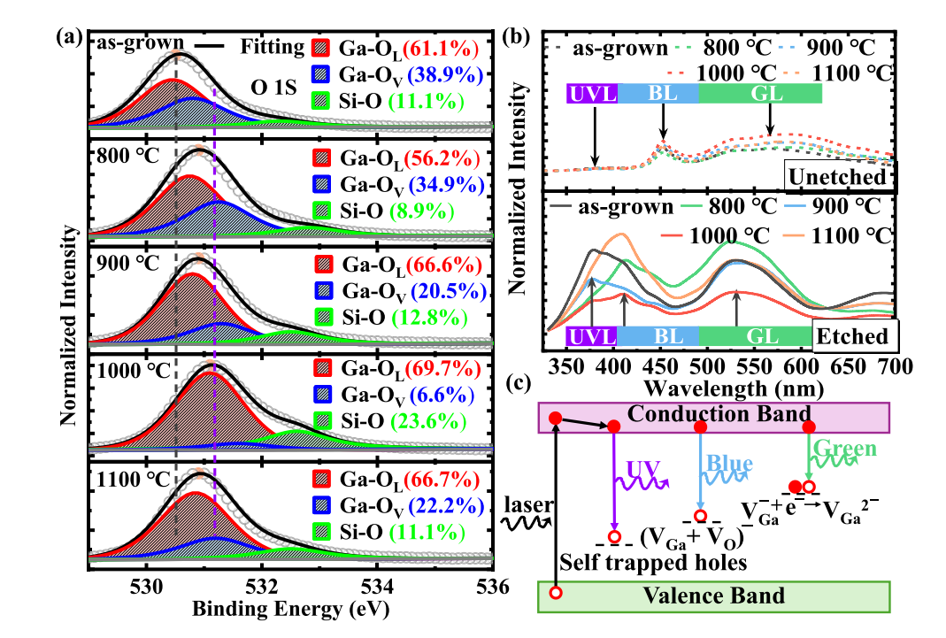
Fig. 5. (a) O 1-s XPS spectra. (b) PL spectra of the unetched and etched β-Ga₂O₃ epitaxial thin films grown on sapphire substrates with different PAT conditions. (c) Schematic energy band diagram showing UVL, BL, and GL emission pathways in β-Ga₂O₃ films.
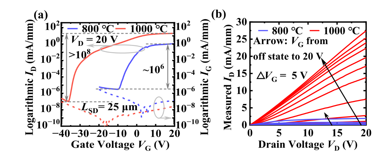
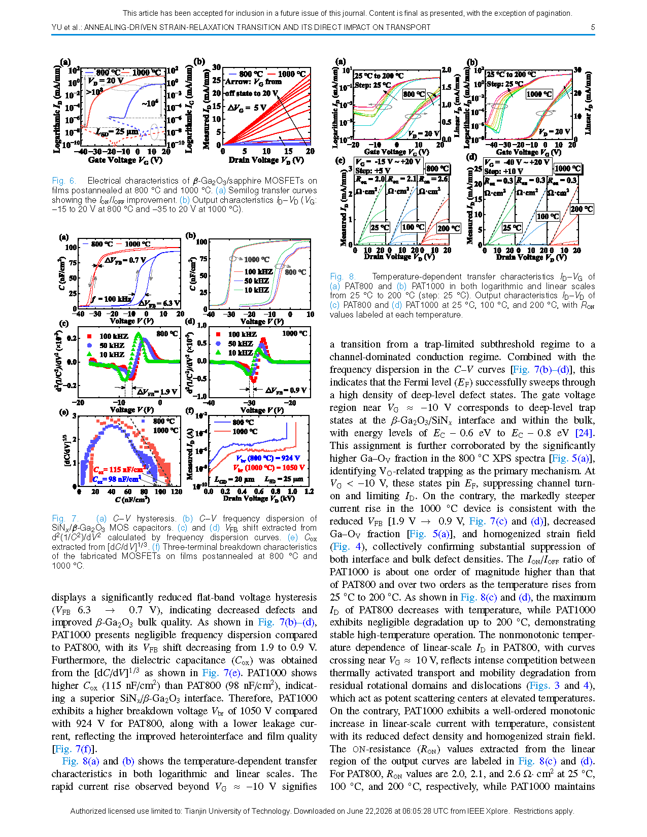
Fig. 6. Electrical characteristics of β-Ga₂O₃/sapphire MOSFETs on films postannealed at 800 ◦C and 1000 ◦C. (a) Semilog transfer curves showing the ION/IOFF improvement. (b) Output characteristics ID-VD (VG −15 to 20 V at 800 ◦C and −35 to 20 V at 1000 ◦C).
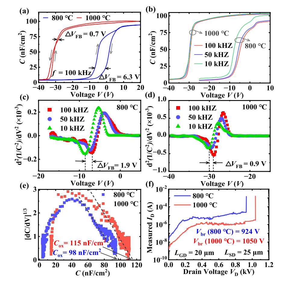
Fig. 7. (a) C–V hysteresis. (b) C–V frequency dispersion of SiNx/β-Ga₂O₃ MOS capacitors. (c) and (d) VFB shift extracted from d²(1/C²)/dV² calculated by frequency dispersion curves. (e) Cox extracted from [dC/dV]^1/3. (f) Three-terminal breakdown characteristics of the fabricated MOSFETs on films postannealed at 800 ◦C and 1000 ◦C.
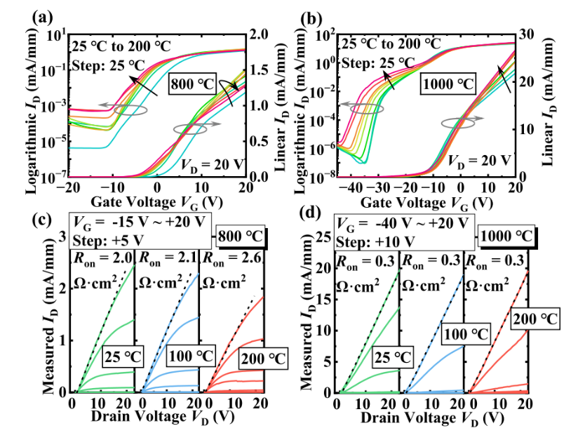
Fig. 8. Temperature-dependent transfer characteristics ID-VG of (a) PAT800 and (b) PAT1000 in both logarithmic and linear scales from 25 ◦C to 200 ◦C (step: 25 ◦C). Output characteristics ID-VD (c) PAT800 and (d) PAT1000 at 25 ◦C, 100 ◦C, and 200 ◦C, with RON values labeled at each temperature.
DOI :
10.1109/TED.2026.3701688
Instruction
Official Account

Cooperation
Top
