


Company Profile
Hangzhou Time-Tech Spectra Co., Ltd. (hereinafter referred to as “Time-Tech Spectra”) was established in 2016 and is headquartered in Hangzhou, China. With transient spectroscopy technology at its core, the company is committed to building a full-stack advanced spectroscopy inspection technology platform covering both scientific instrumentation and industrial inspection.
In the industrial application sector, Time-Tech Spectra has developed the world’s first nondestructive inspection system for compound semiconductor wafer defects based on transient spectroscopy technology, which has gained broad recognition from leading customers in China and overseas. The company is currently continuing to expand its product portfolio to meet emerging material inspection needs, accelerating the R&D and market introduction of defect inspection equipment for compound semiconductor materials, and leveraging innovative technologies to empower the global semiconductor supply chain.
The company’s R&D team combines strong academic backgrounds with extensive industrialization experience. It currently comprises 21 Ph.D. holders and 49 master’s degree holders, with each of its four major business segments led by experts with more than 10 years of R&D and engineering experience. The team has participated in a number of major national-level R&D projects.
To date, the company has been granted 29 invention patents, 2 PCT patents, 21 utility model patents, and 33 software copyrights, establishing a relatively comprehensive independent intellectual property portfolio.
In the SiC sector, Time-Tech Spectra has developed a systematic portfolio of optical nondestructive inspection products covering the substrate, epitaxy, and device stages. Products including DISPEC-9000, TAU-9000HR, and SR-9000 have been validated by leading customers in China and overseas and have achieved continued repeat orders. The company has established comprehensive inspection capabilities spanning defect inspection, minority-carrier lifetime measurement, and laser aging testing.
As the SiC industry chain continues to mature and inspection requirements become increasingly sophisticated, Time-Tech Spectra is extending its established optical nondestructive inspection technologies to other compound semiconductor materials, including GaN, Ga₂O₃, InP, and GaAs. For gallium oxide, in particular, the company has launched dedicated optical nondestructive inspection equipment, further expanding its inspection capabilities for emerging wide-bandgap semiconductor materials.
Core Product for the Ga₂O₃ Sector: SN-9000 Ga₂O₃ Wafer Dislocation Nondestructive Inspection System
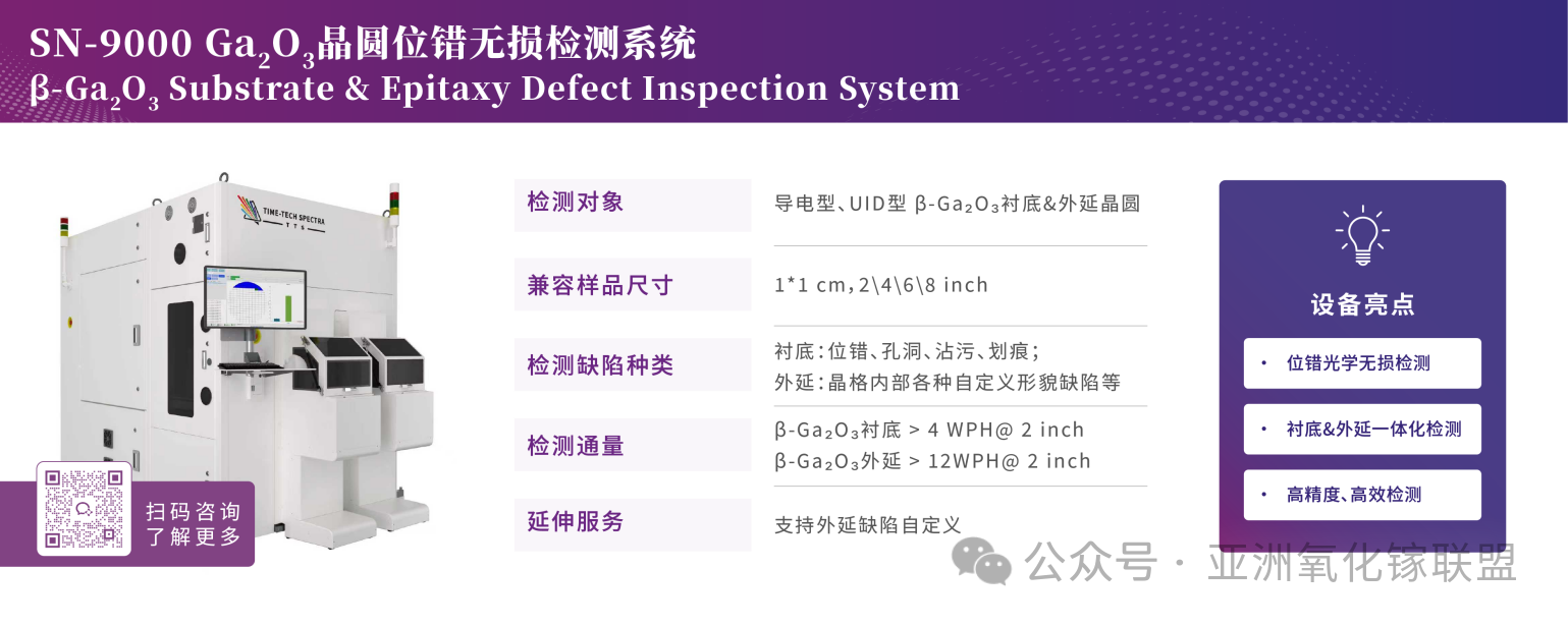
To address the inspection requirements of gallium oxide substrates and epitaxial materials in defect identification, quality control, and process optimization, Time-Tech Spectra has developed the SN-9000 Ga₂O₃ Wafer Dislocation Nondestructive Inspection System.
Focusing on the two critical stages of substrate and epitaxy, the system provides comprehensive capabilities covering defect detection, identification, localization, and correlation analysis, with the following five core advantages:
01|Optical Nondestructive Inspection for 100% Wafer and Batch Inspection
The system employs optical nondestructive dislocation inspection technology, enabling precise identification of internal defects without damaging the sample. This not only ensures the integrity and reliability of inspection results, but also avoids the loss of costly substrates and epitaxial wafers. It is particularly well suited for batch release inspection and R&D validation of high-value β-Ga₂O₃ materials.
02|Integrated Substrate + Epitaxy Inspection for One-Stop Quality Control
The system supports integrated inspection of both substrates and epitaxial wafers on a single platform, eliminating the need to switch between different inspection systems. It enables full-process quality monitoring from wafer substrates to epitaxial layers, significantly shortening material transfer cycles, reducing the risk of cross-contamination, and improving production-line efficiency.
03|High Precision + High Throughput, Balancing Quality and Capacity
The system can clearly distinguish dislocations, voids, contamination, scratches, and various customizable morphological defects within epitaxial layers. The inspection throughput exceeds 4 WPH for 2-inch β-Ga₂O₃ substrates and 12 WPH for 2-inch epitaxial wafers, maintaining a leading position within the same precision class and meeting the stringent speed requirements of high-volume production lines.
04|Broad Size Compatibility for Flexible Process Integration
The system is compatible with 1 × 1 cm² small samples and standard 2-, 4-, 6-, and 8-inch wafers, covering the full range of inspection needs from R&D-scale samples to high-volume manufacturing. Its multi-size compatibility enables one system to serve multiple applications, helping reduce repeated equipment investment.
05|Customized Epitaxial Defect Identification + Defect Traceability
The system accurately captures various morphological defects in Ga₂O₃ epitaxial layers and incorporates customized defect-recognition capabilities to help manufacturers trace defect origins and continuously optimize epitaxial processes.
Leveraging its integrated substrate-and-epitaxy inspection capability and submicron-level positioning accuracy, the system can precisely correlate defect locations across the two layers. This enables direct visualization of how defects propagate from the substrate into the epitaxial layer, facilitating root-cause analysis and providing actionable feedback for the iterative optimization of Ga₂O₃ substrate preparation and epitaxial growth processes.
Global First: Time-Tech Spectra’s SN-9000 Ga₂O₃ Wafer Dislocation Nondestructive Inspection System Officially Delivered
In 2026, Time-Tech Spectra’s independently developed SN-9000 Ga₂O₃ Wafer Dislocation Nondestructive Inspection System was officially shipped and successfully delivered to a leading customer in the industry, marking the world’s first commercial deployment of such a system.
This milestone represents a significant breakthrough for Time-Tech Spectra in the field of inspection technologies for fourth-generation semiconductor materials.

Development Plans
Time-Tech Spectra has established a comprehensive product portfolio covering scientific instrumentation, semiconductor wafer inspection, and photovoltaic cell inspection. In the compound semiconductor sector, the company focuses on inspection technologies for materials including SiC, GaN, Ga₂O₃, InP, and GaAs, while continuously expanding the application of optical inspection technologies across different materials and process stages.
In the Ga₂O₃ sector, the company is continuously strengthening its capabilities in nondestructive inspection, defect identification and localization, and substrate–epitaxy defect correlation analysis in response to the inspection requirements of industrialization. These capabilities are intended to provide technical support for Ga₂O₃ material R&D, substrate preparation, epitaxial growth, and high-volume manufacturing.
At the same time, the company will strengthen technical exchanges and collaboration with universities, research institutes, material manufacturers, and device companies. By deepening industry–academia–research collaboration in areas such as Ga₂O₃ material defect inspection, quality evaluation, and process optimization, Time-Tech Spectra aims to further integrate advanced inspection technologies with the practical needs of the Ga₂O₃ industry.
Instruction
Official Account

Cooperation
Top
