


Researchers from the Shenzhen Pinghu Laboratory and Shandong University have published a paper titled "Fe-Doped β-Ga₂O₃ Photoconductive Switches with High Conversion Efficiency and Fast Rise Time under Sub-Bandgap Excitation" in Applied Physics Letters.
Background
Photoconductive semiconductor switches (PCSS) serve as essential components for next-generation pulsed power systems, featuring inherent merits including optical isolation, ultrafast triggering, and compact system integration. β-Ga₂O₃ is an ultra-wide-bandgap semiconductor with a bandgap of ~ 4.8 eV and a theoretical breakdown field up to 8 MV/cm, making it a promising candidate for high-voltage and high-power PCSS. Large-area single-crystal substrates fabricated by melt-growth techniques further boost its engineering prospects. Conventional wide-bandgap semiconductors such as SiC and GaN can utilize above-bandgap illumination to generate photocarriers for switch operation. For β-Ga₂O₃, intrinsic band-to-band excitation requires deep-ultraviolet light sources with high cost and limited output power, which hinders practical deployment. Fe doping compensates residual carriers and introduces deep acceptor states to enable sub-bandgap triggered switching. Nevertheless, carrier dynamics in Fe-doped β-Ga₂O₃ under sub-bandgap excitation remain poorly understood, especially under high-injection and high-field conditions. Thermal-induced device degradation under high optical excitation also needs systematic investigation to guide device design for high-performance β-Ga₂O₃ PCSS.
Abstract
β-Ga₂O₃ photoconductive semiconductor switches (PCSS) hold immense promise for high-power optically controlled switching, yet the carrier dynamics under sub-bandgap excitation remain insufficiently understood, especially in the high-injection, high-field regime. Herein, we systematically investigated the carrier behavior of Fe-doped β-Ga₂O₃ PCSS under 355 nm sub-bandgap excitation. The device demonstrates a voltage conversion efficiency as high as 83.9% and an on-state resistance as low as 9.6 Ω, while maintaining a fast rise time of ~250 ps. Further analysis indicates that thermal effects limit further performance improvement under high excitation. This work provides insight into defect-mediated carrier dynamics in β-Ga₂O₃ and highlights its potential for high-efficiency and high-speed photoconductive switching under sub-bandgap excitation.
Highlights
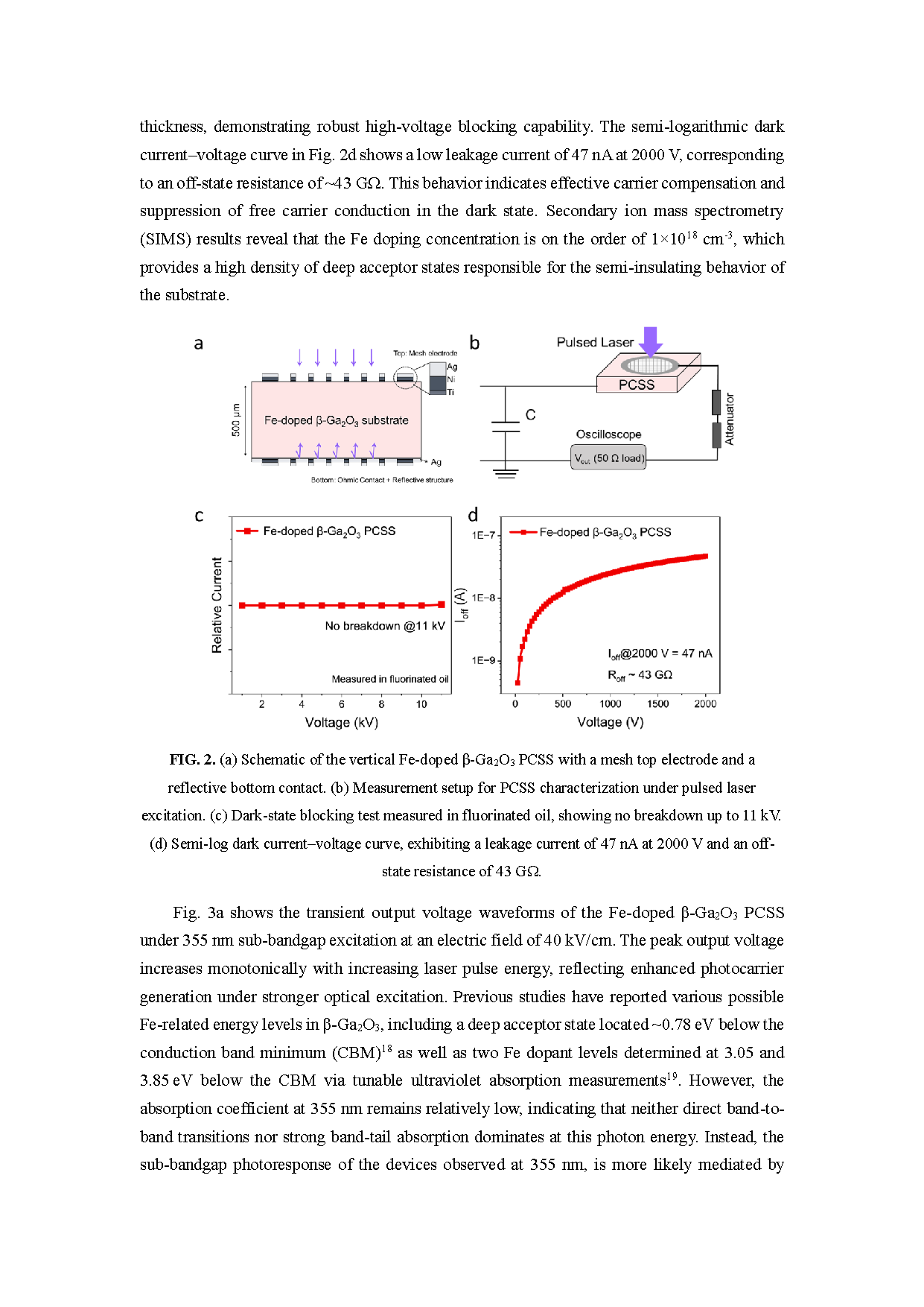
Vertical-structured Fe-doped β-Ga₂O₃ photoconductive semiconductor switch is fabricated with mesh top electrode and reflective bottom contact, realizing efficient volumetric carrier generation and high-field operation. The device sustains blocking voltage up to 11 kV with off-state resistance of ~43 GΩ.
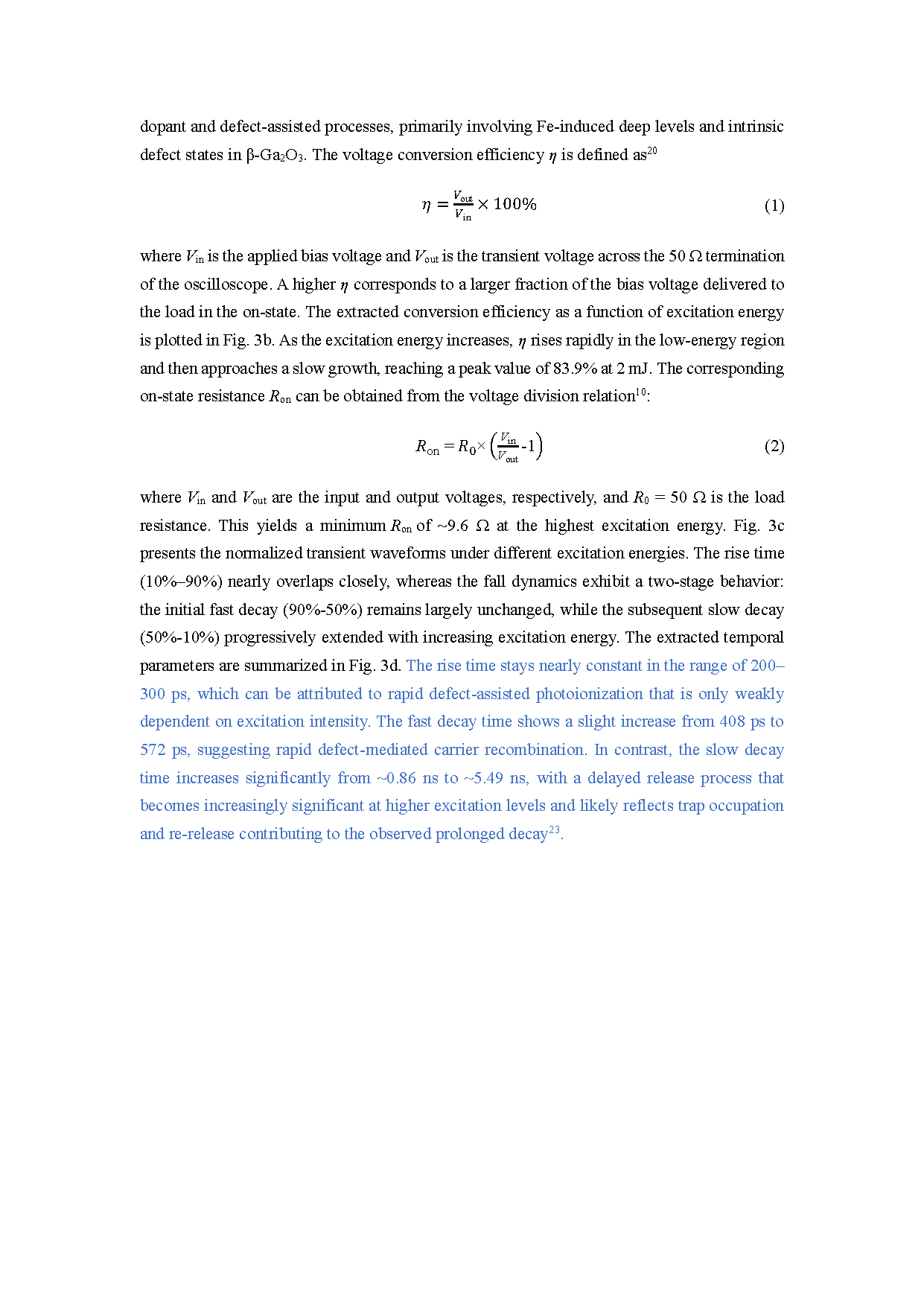
A high voltage conversion efficiency of 83.9 % and low on-state resistance of 9.6 Ω are achieved under 355 nm sub-bandgap laser excitation, while keeping fast rise time of ~250 ps. The rise time is nearly independent of excitation laser energy.
Two-stage decay dynamics are observed in transient response. The slow decay component elongates obviously with increased excitation energy originating from trap capture-re-release effect, clarifying the modulation effect of defect states on transient switching performance.
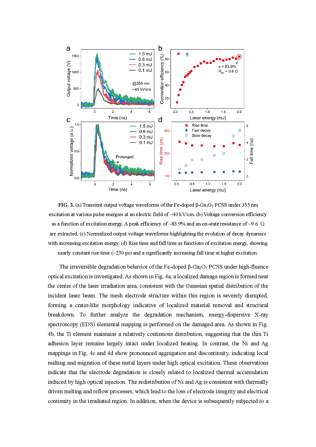
Irreversible device degradation originating from metal electrode melting-migration and local thermal accumulation under high-fluence optical excitation is demonstrated, identifying thermal effect as the key bottleneck limiting performance ceiling.
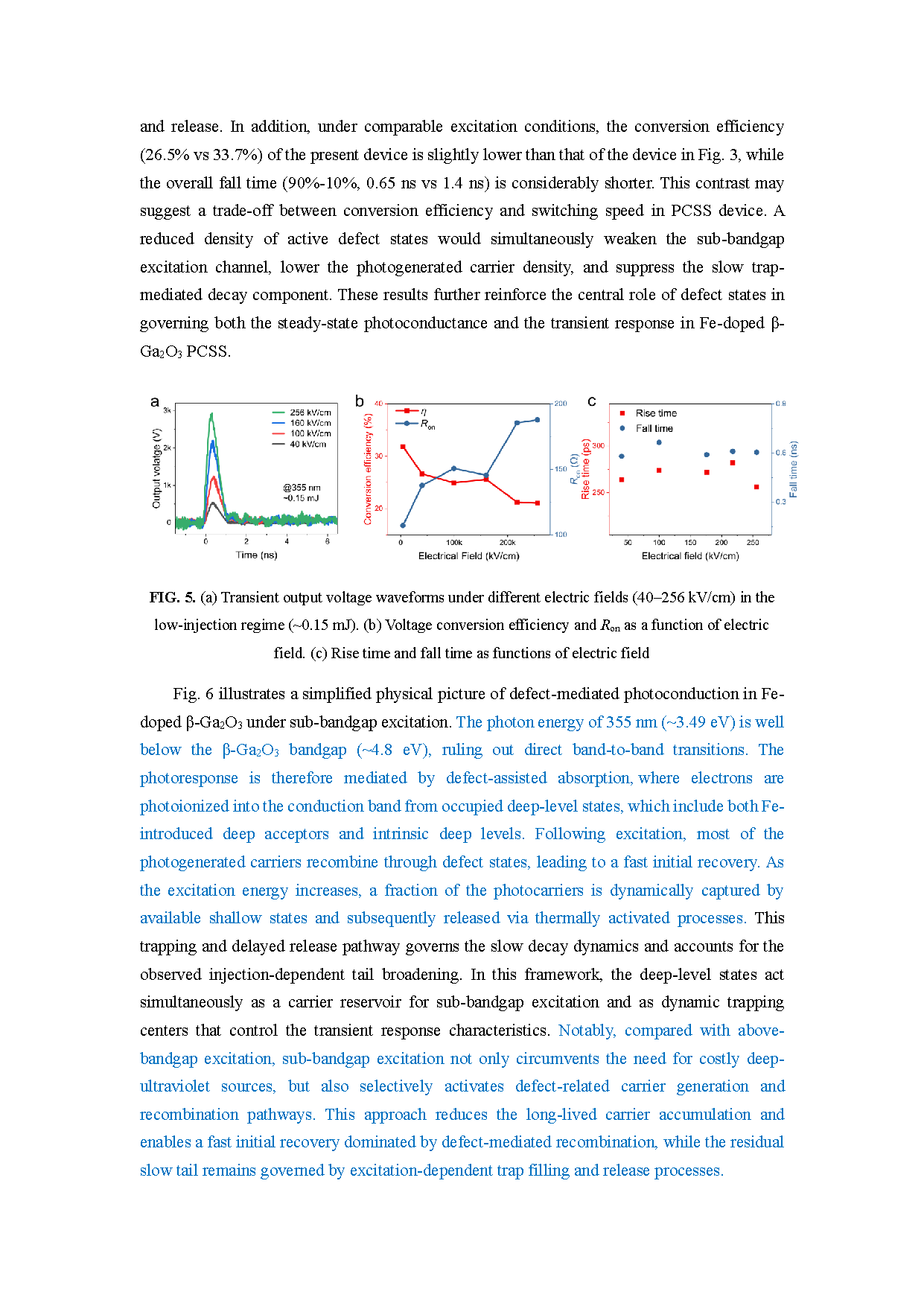
Low-injection measurements under varied electric fields are performed to analyze the evolution of conversion efficiency and on-state resistance, providing experimental reference for engineering design of sub-bandgap triggered β-Ga₂O₃ PCSS.
Conclusion
In summary, we systematically investigated the defect-regulated carrier dynamics in Fe-doped β-Ga₂O₃ photoconductive semiconductor switches under 355 nm sub-bandgap excitation. The device exhibits a high voltage conversion efficiency of up to 83.9% and a fast rise time of ~250 ps, demonstrating the effectiveness of defect-assisted photoconduction for high-performance switching in dopant-engineered β-Ga₂O₃. The rise time and the initial fast decay time show weak dependence on excitation conditions, whereas the subsequent slow decay time is strongly influenced by defect states participating in carrier capture and delayed release processes. Further failure analysis identifies thermal management as the critical bottleneck limiting further performance improvement in β-Ga₂O₃ PCSS. These results provide insight into sub-bandgap carrier dynamics in ultrawide-bandgap semiconductors and offer guidance for the design of high-efficiency and high-speed optically controlled switches.
Project Support
We acknowledge the support from the Shenzhen Pinghu Laboratory Project (Grant No. 225190 and 925060).
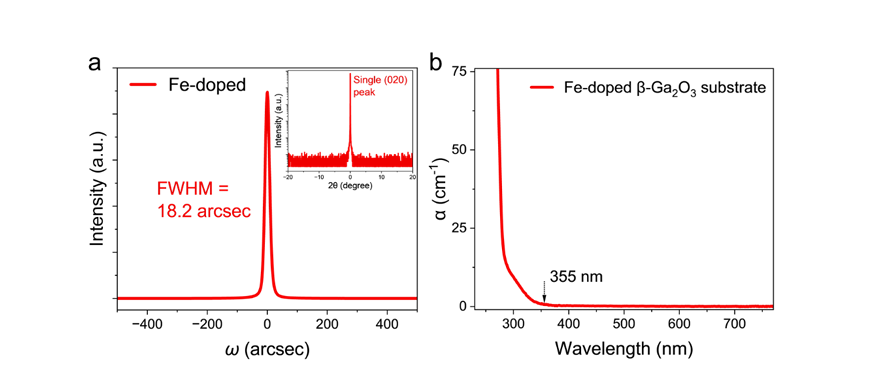
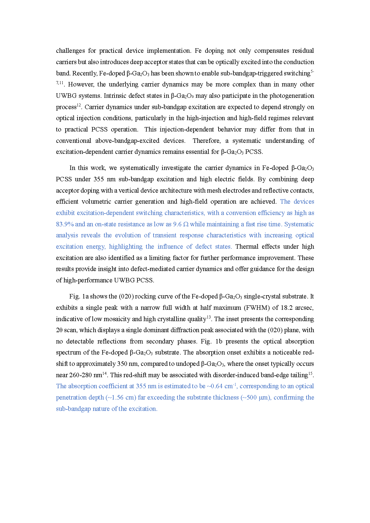
Figure 1. (a) Rocking curve of the Fe-doped β-Ga₂O₃ substrate, showing a FWHM of 18.2 arcsec. The inset shows the XRD 2θ scan, displaying a single (020) diffraction peak. (b) Optical absorption coefficient spectrum of the Fe-doped β-Ga₂O₃ substrate. The absorption onset is red-shifted to ~350 nm; the 355 nm excitation wavelength used in this work is indicated. The inset schematically shows the tail states involved in Fe-doped β-Ga₂O₃.
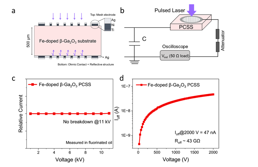
Figure 2. (a) Schematic of the vertical Fe-doped β-Ga₂O₃ PCSS with a mesh top electrode and a reflective bottom contact. (b) Measurement setup for PCSS characterization under pulsed laser excitation. (c) Dark-state blocking test measured in fluorinated oil, showing no breakdown up to 11 kV. (d) Semi-log dark current-voltage curve, exhibiting a leakage current of 47 nA at 2000 V and an off-state resistance of 43 GΩ.
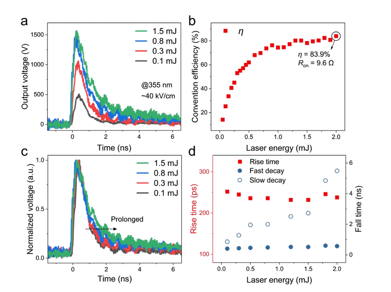
Figure 3. (a) Transient output voltage waveforms of the Fe-doped β-Ga₂O₃ PCSS under 355 nm excitation at various pulse energies at an electric field of ~40 kV/cm. (b) Voltage conversion efficiency as a function of excitation energy. A peak efficiency of ~83.9% and an on-state resistance of ~9.6 Ω are extracted. (c) Normalized output voltage waveforms highlighting the evolution of decay dynamics with increasing excitation energy. (d) Rise time and fall time as functions of excitation energy, showing nearly constant rise time (~250 ps) and a significantly increasing fall time at higher excitation.
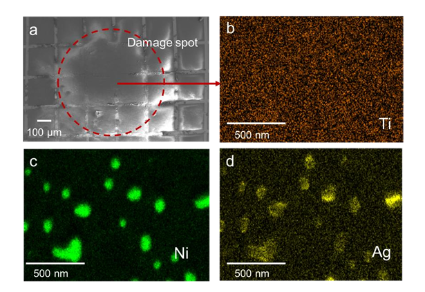
Figure 4. (a) SEM image of the mesh electrode region after high optical excitation, showing a localized burnout spot (circular dashed outline). (b)-(d) EDS elemental mapping of the damaged area: (b) Ti exhibiting a relatively continuous distribution across the burnout region; (c) Ni and (d) Ag layers display pronounced aggregation into isolated clusters and co-localization within the damaged zone, indicative of melting driven by excessive local heating.
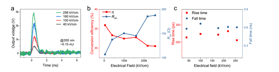
Figure 5. (a) Transient output voltage waveforms under different electric fields (40-256 kV/cm) in the low-injection regime (~0.15 mJ). (b) Voltage conversion efficiency and Ron as a function of electric field. (c) Rise time and fall time as functions of electric field.

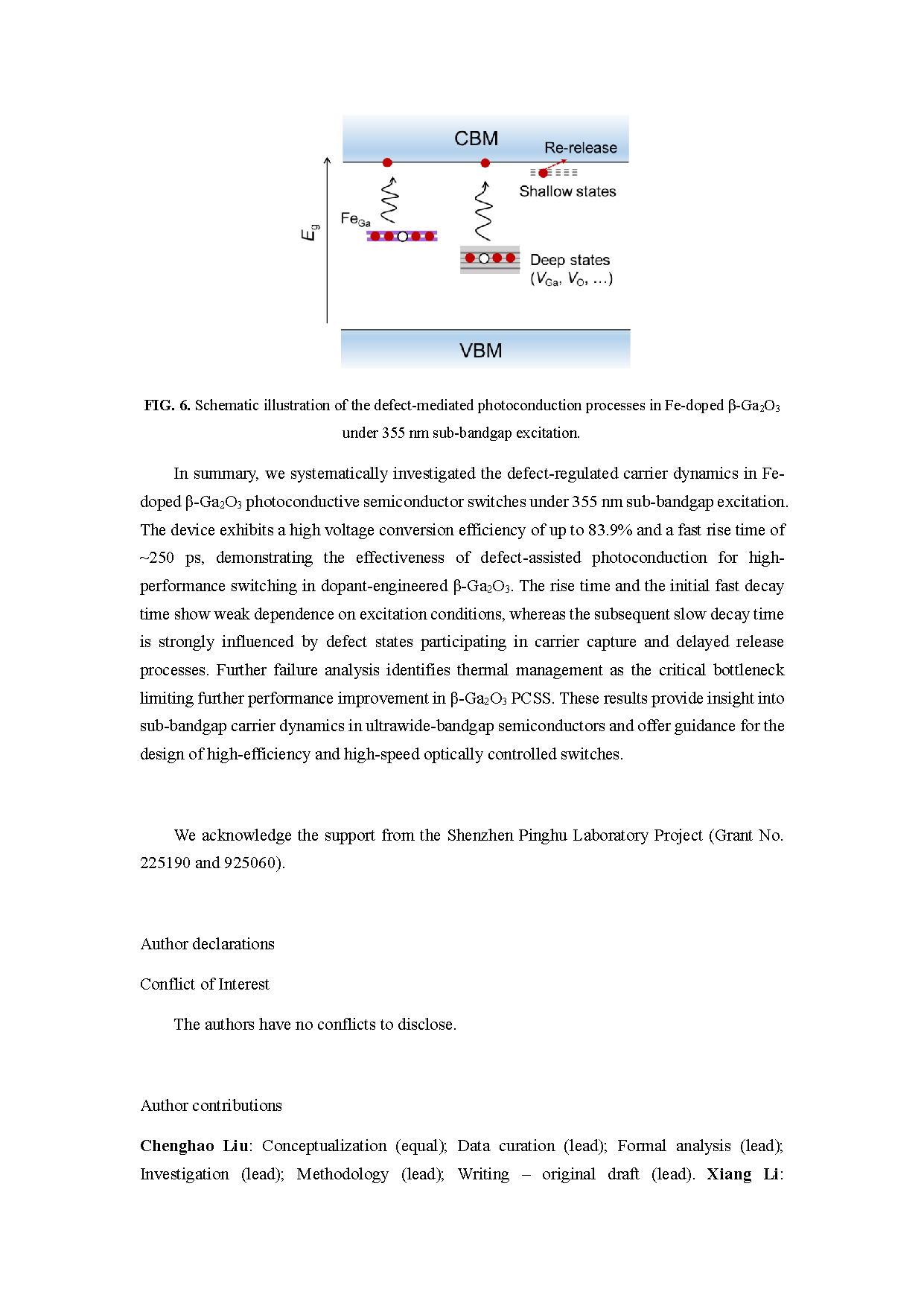
Figure 6. Schematic illustration of the defect-mediated photoconduction processes in Fe-doped β-Ga₂O₃ under 355 nm sub-bandgap excitation.
DOI:
doi.org/10.1063/5.0344550
Instruction
Official Account

Cooperation
Top
