


Westlake University School of Engineering Researcher Wei Kong's Team Makes Significant Progress in Atomic-Scale Ferroelectric Thin Films, Achieving Stable Ferroelectric Polarization in Sub-Nanometer-Thick (6 Å) Single-Crystal Two-Dimensional Gallium Oxide (2D-Ga₂O₃) for the First Time, Providing a Novel Material System for Ultra-Low-Power, High-Density Memory Devices. The related findings are published in Nature Electronics under the title "Ferroelectricity in six-angstrom-thick two-dimensional gallium oxide."
Ferroelectric materials, owing to their reversible polarization switching under an external electric field, hold significant promise for applications in non-volatile memory, neuromorphic computing, and sensing. As microelectronic devices continue to scale toward higher integration density and lower power consumption, ferroelectrics are considered a critical candidate material system for next-generation memory-computing fusion architectures. Particularly in the context of ever-shrinking device dimensions, developing ferroelectric materials that can operate reliably at the nanometer or even atomic scale is of great importance for achieving ultra-high-density integration and novel computing paradigms.
However, when ferroelectric materials are scaled down to nanometer or even atomic thicknesses, their performance becomes severely constrained by size effects. On one hand, the enhanced depolarization field arising from uncompensated surface charges at the film surface can severely weaken or even suppress ferroelectric polarization. On the other hand, in ultrathin ferroelectric films, confined domain structures and enhanced interfacial pinning effects make polarization switching increasingly difficult, leading to a significant increase in the required operating voltage. This not only compromises device reliability and power consumption but also makes it challenging to meet the stringent low-voltage requirements (typically below 1 V) of advanced CMOS technologies. Therefore, achieving both stable ferroelectric polarization retention and low-voltage switching at the ultimate thickness limit has become a core challenge in the research and device application of ultrathin ferroelectrics.
To address the above challenges, the research team innovatively proposed a "self-limited exfoliation + strain engineering" strategy: by modulating the epitaxial interface, they achieved self-limited exfoliation of β-Ga₂O₃ films from a homoepitaxial substrate, thereby obtaining large-area, high-quality two-dimensional single-crystalline films with a minimum thickness of only half a unit cell (6 Å). Simultaneously, strain was introduced into the films to induce a structural transition from the centrosymmetric β-phase to the non-centrosymmetric ferroelectric phase (FE-ZB phase), thereby generating stable ferroelectric polarization at the ultimate thickness limit. Experiments demonstrate that this 2D-Ga₂O₃ exhibits clear ferroelectric hysteresis characteristics even at sub-nanometer thickness (6 Å), with a remnant polarization of approximately 7.5 μC/cm², along with excellent polarization retention and thermal stability (Curie temperature exceeding 1300 K). Furthermore, by tuning the strain magnitude, the polarization switching voltage was successfully reduced to 0.8 V, achieving a voltage scale compatible with advanced CMOS processes. In addition, the team demonstrated the compatibility of ferroelectric 2D-Ga₂O₃ with Si-based back-end-of-line (BEOL) processes. These findings position 2D-Ga₂O₃ as a material with great potential for realizing multi-functionality—including computing, memory, and sensing—within a single architecture, making it an ideal candidate for next-generation high-density, low-power multifunctional integrated electronics.

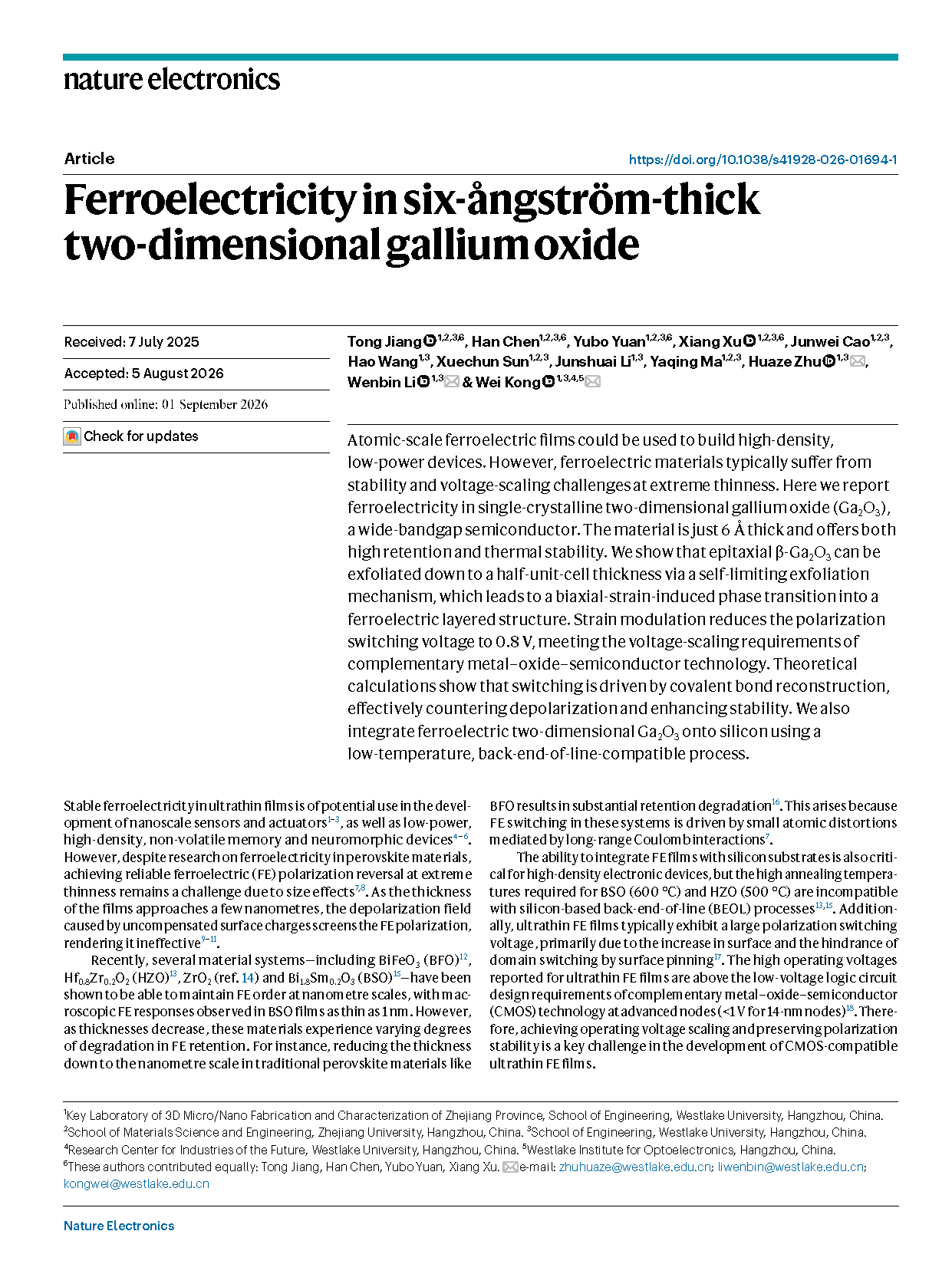
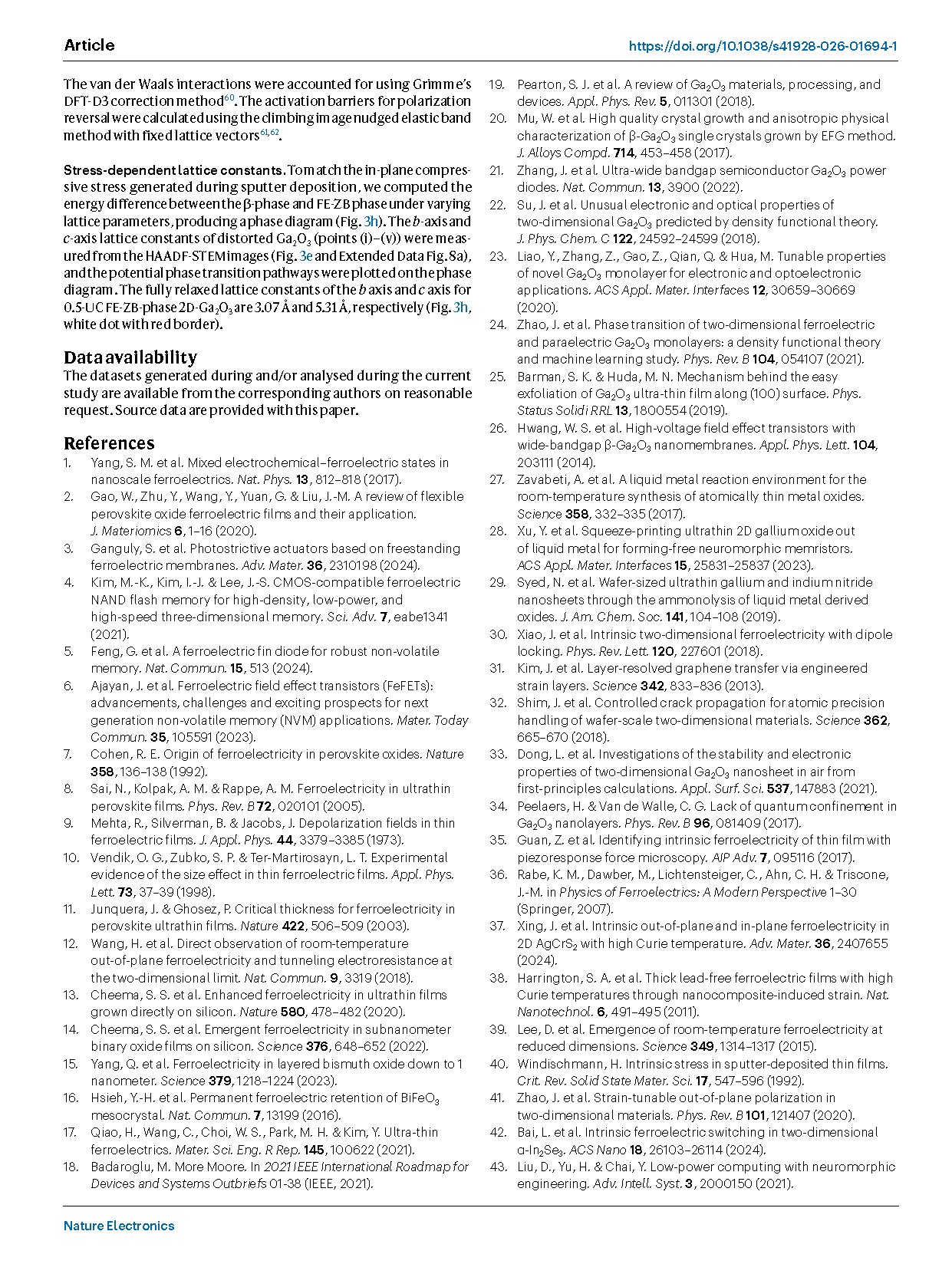
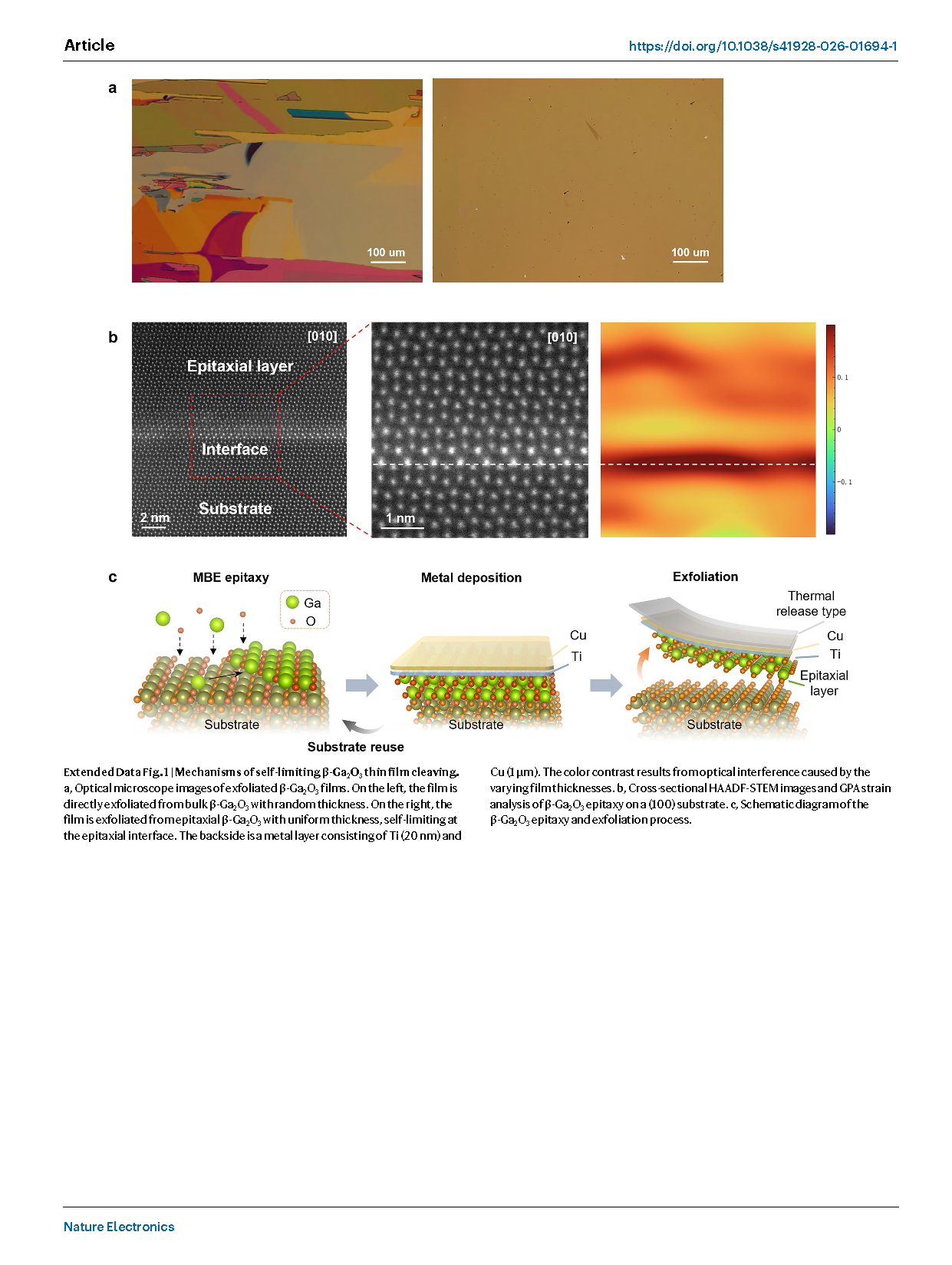
Figure 1. Synthesis of single-crystal β-Ga₂O₃ films with different thicknesses.
Optical microscopy and high-resolution transmission electron microscopy (HRTEM) confirm the controllable synthesis of large-area single-crystal β-Ga₂O₃ films with varying thicknesses via the self-limited exfoliation strategy, with the thinnest films reaching 0.5 unit cell thickness (6 Å).
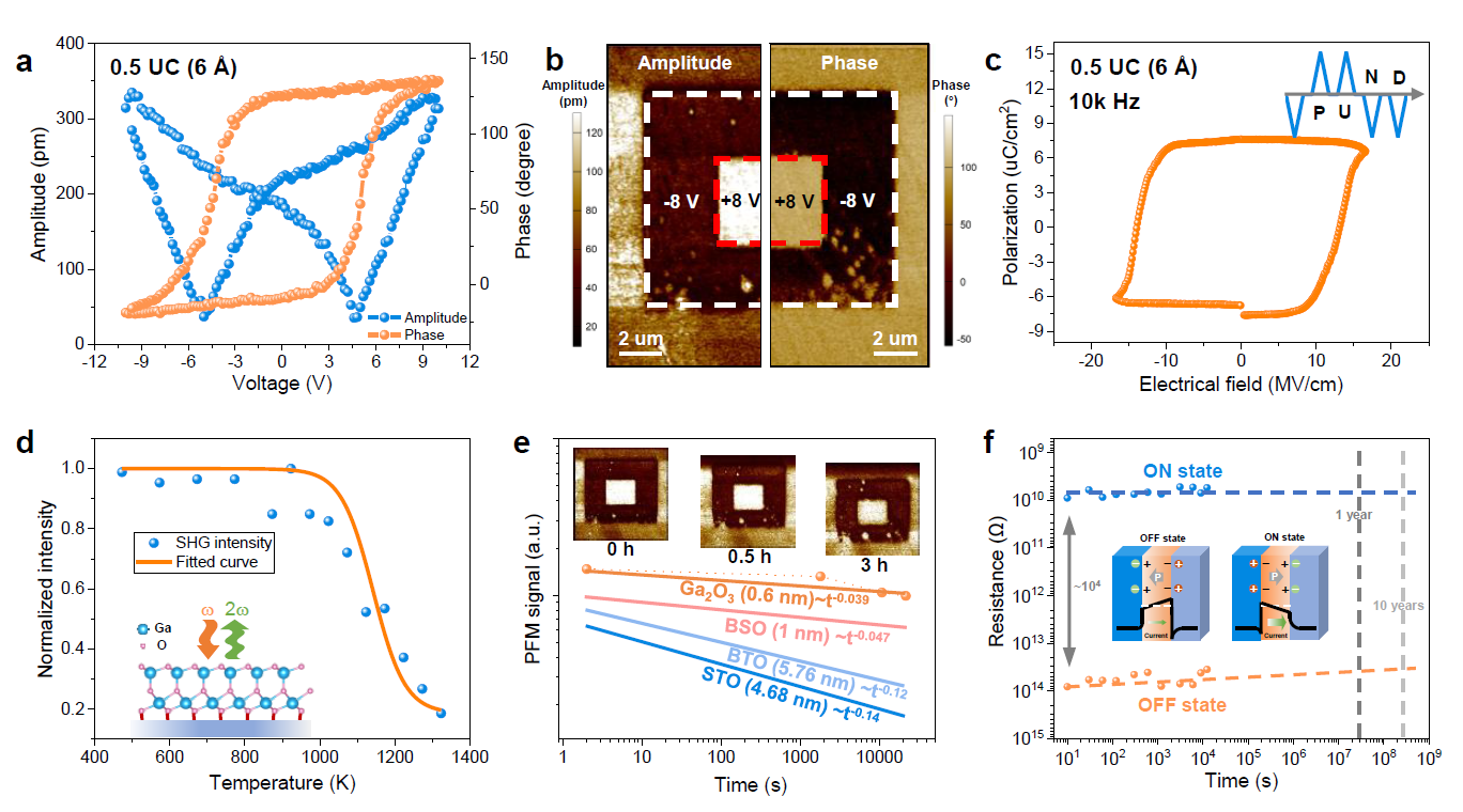
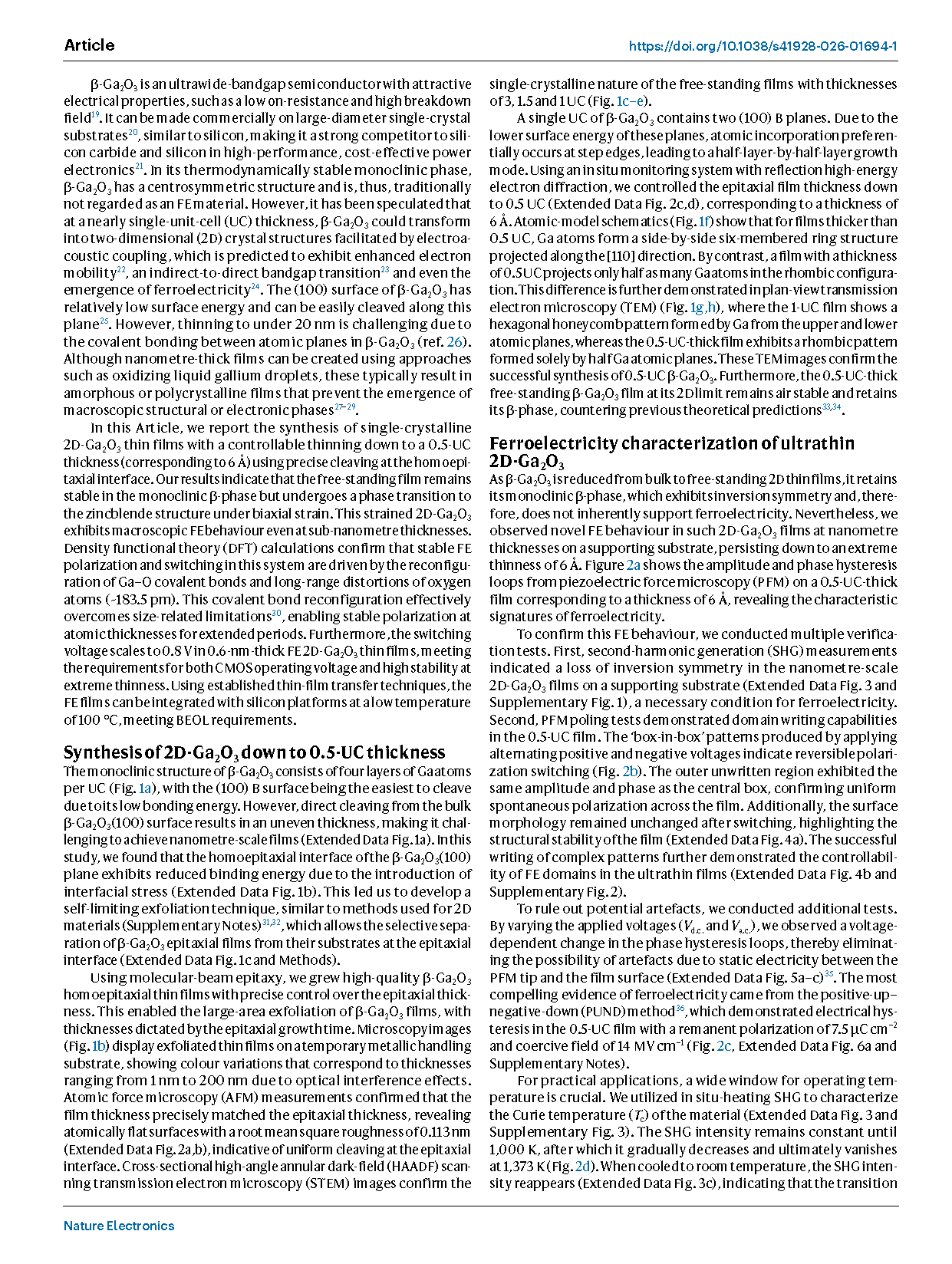
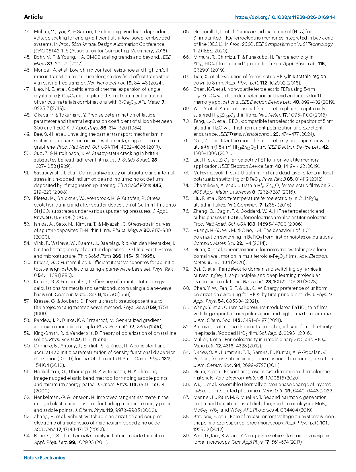
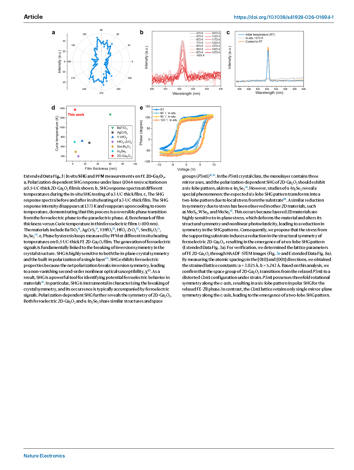
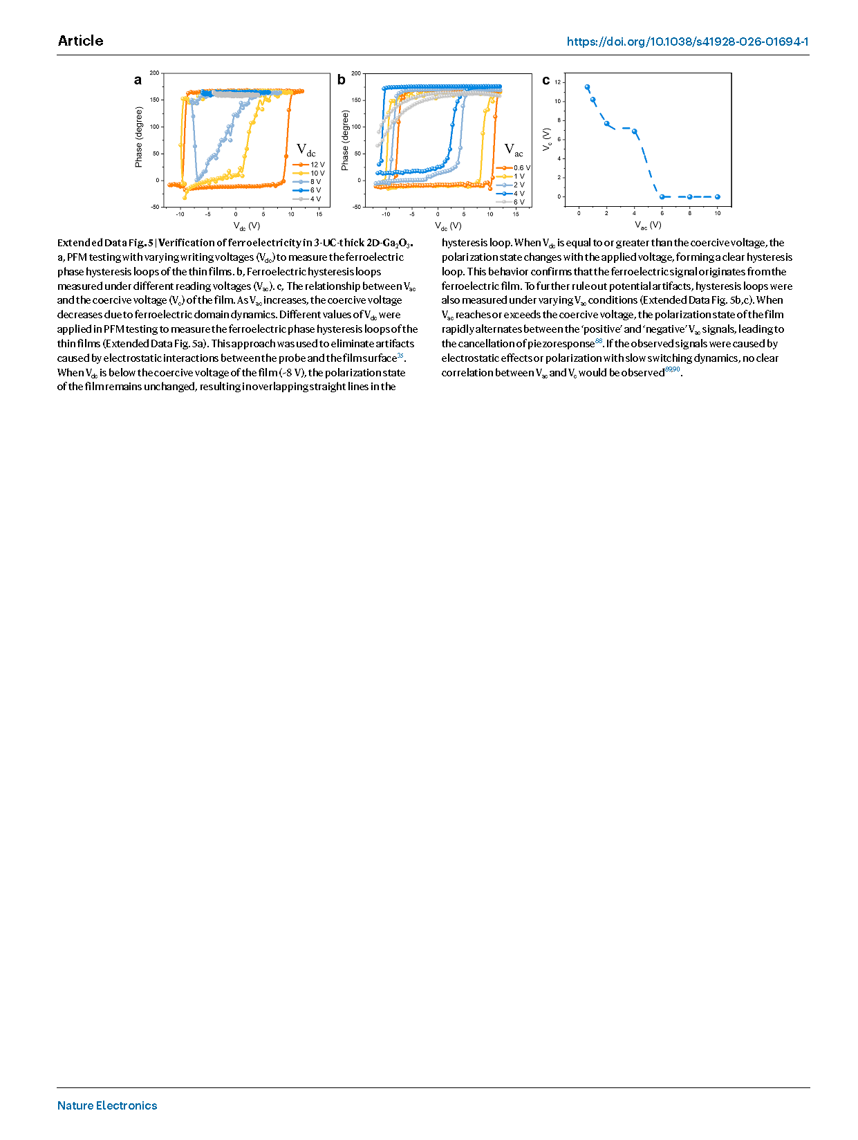
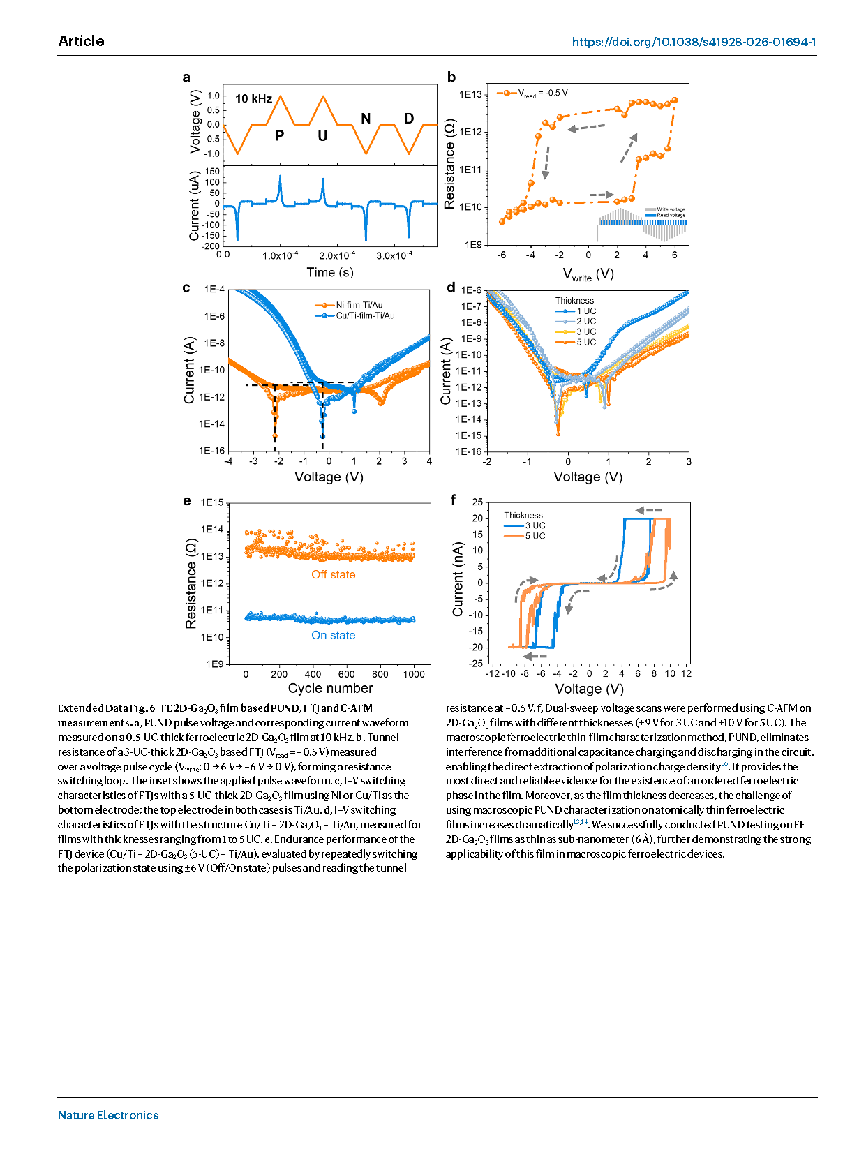
Figure 2. Ferroelectric characterization of ultrathin 2D-Ga₂O₃ films.
Piezoresponse force microscopy (PFM) and PUND measurements confirm the existence of ferroelectric polarization in 6 Å-thick 2D-Ga₂O₃ films, and second harmonic generation (SHG) signals indicate a Curie temperature exceeding 1300 K. Ferroelectric tunnel junction devices fabricated from these films exhibit an ON/OFF resistance ratio exceeding 10⁴ and excellent polarization stability.
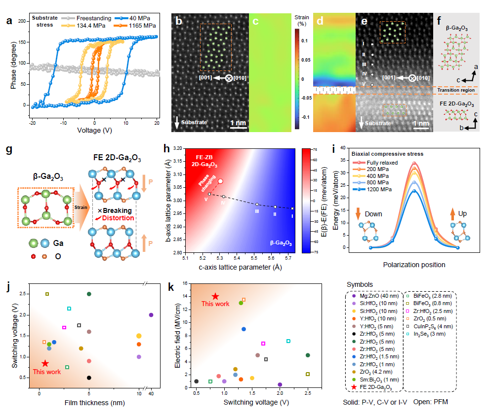
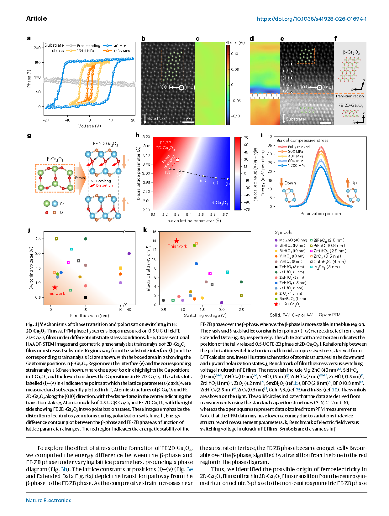
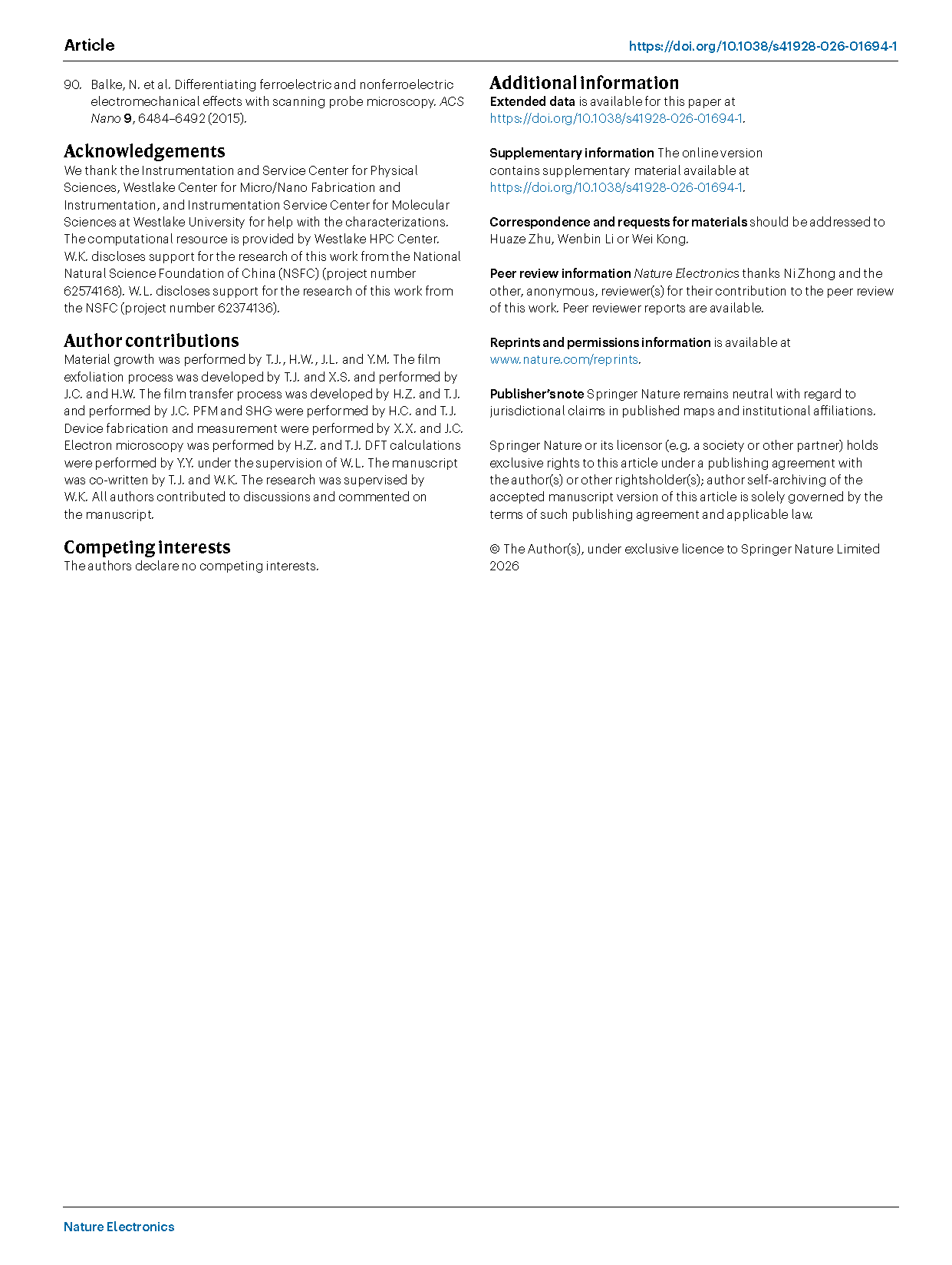
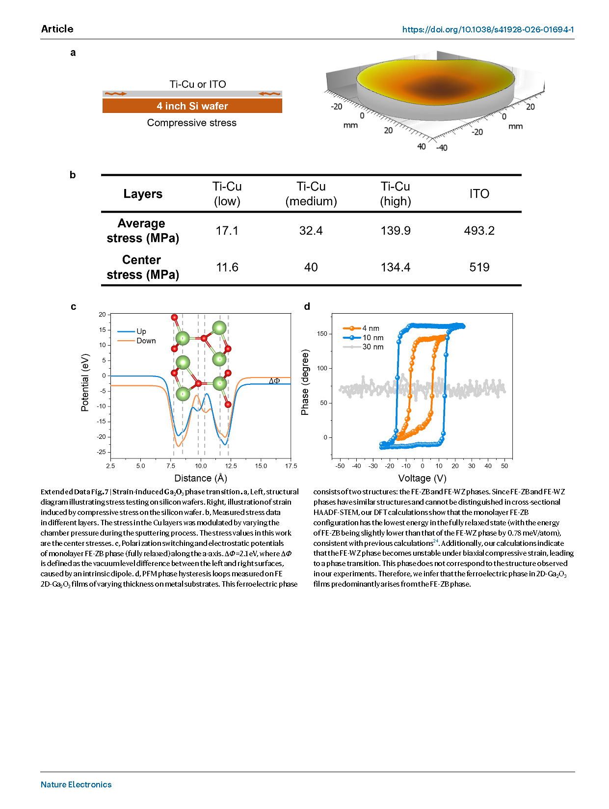
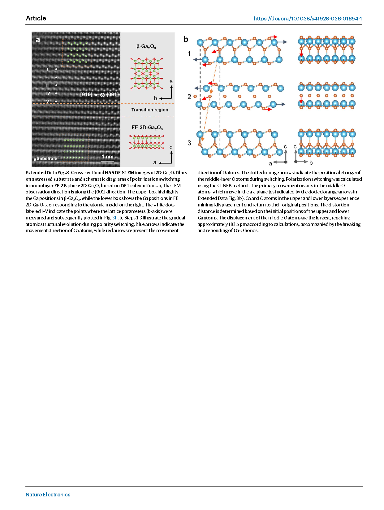
Figure 3. Phase transition and polarization switching mechanisms of ferroelectric 2D-Ga₂O₃ films.
Combining density functional theory (DFT) calculations with experimental observations (PFM under varying stress and TEM atomic-scale imaging), the strain-induced ferroelectric phase transition mechanism in ultrathin 2D-Ga₂O₃ films is revealed. A polarization switching mechanism based on covalent bond reconstruction is proposed, providing theoretical support for the excellent polarization stability of the films. Moreover, the polarization switching barrier of 2D-Ga₂O₃ films is tunable by stress, enabling a low switching voltage (0.8 V) while maintaining high polarization stability.
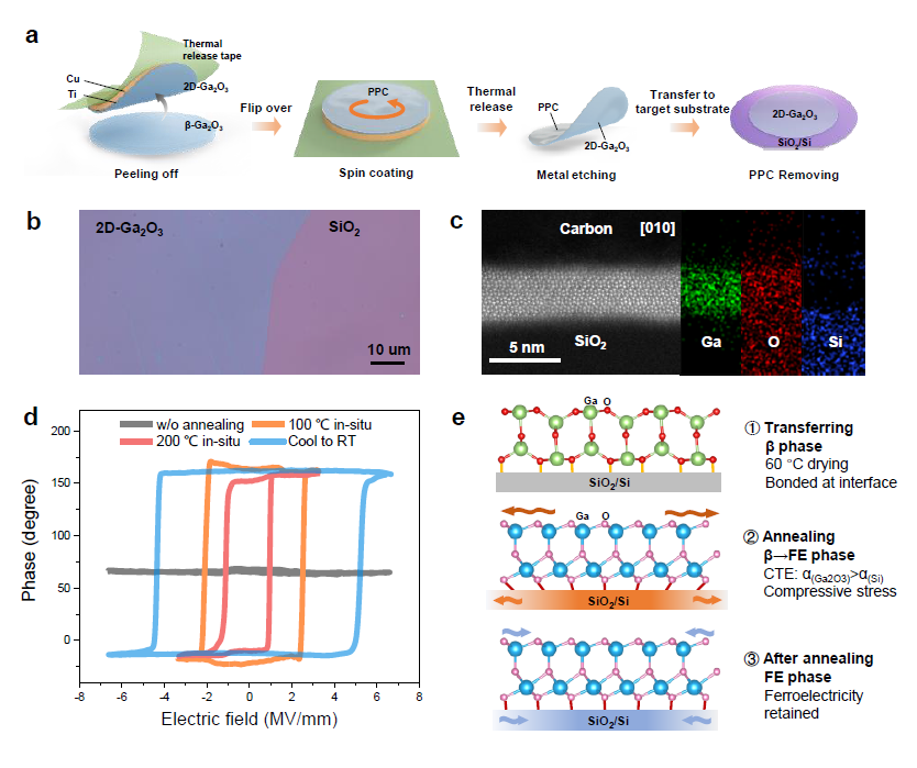
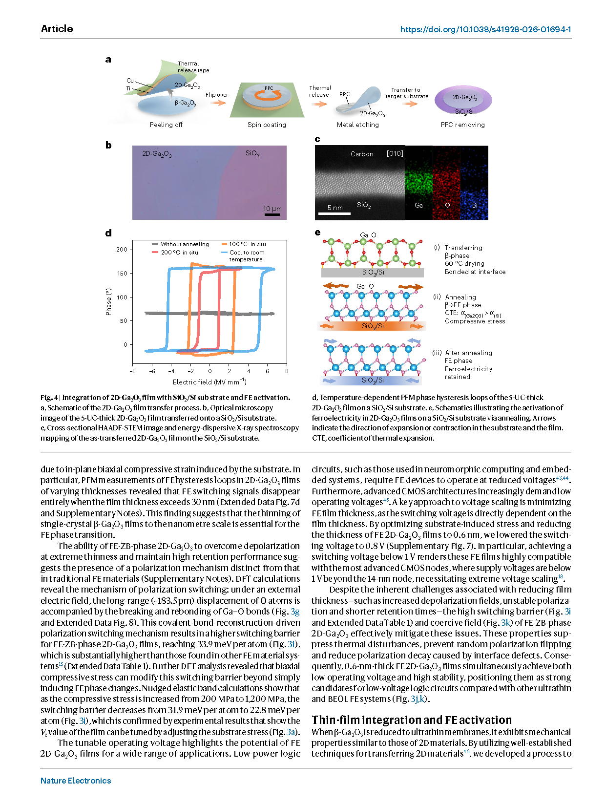
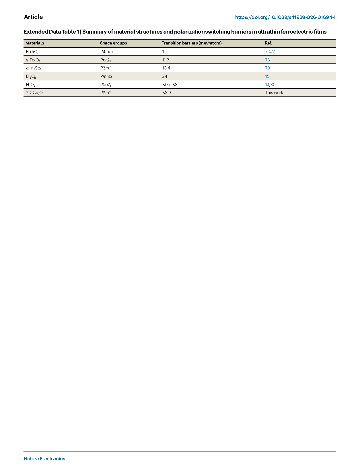
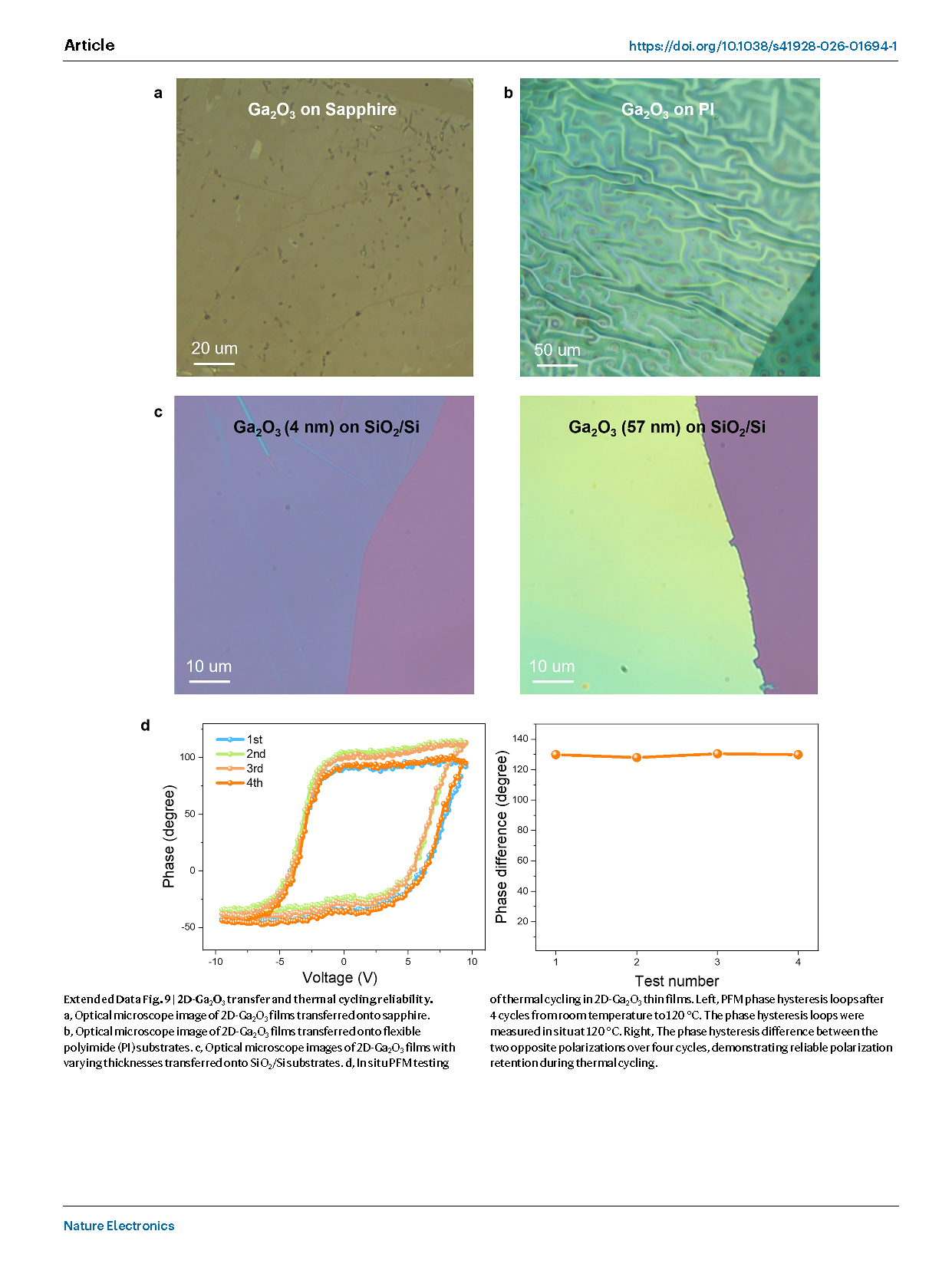
Figure 4. Integration of 2D-Ga₂O₃ films with SiO₂/Si substrates and ferroelectric activation.
Through film transfer technology, 2D-Ga₂O₃ films are successfully integrated with various substrates. Ferroelectric activation of 2D-Ga₂O₃ films on Si is achieved via a low-temperature annealing process compatible with Si-based BEOL processes, demonstrating the multi-substrate compatibility of 2D-Ga₂O₃ films and their integration potential in silicon-based electronics.
Highlights of this study:
Controllable preparation of 6 Å-thick single-crystal 2D-Ga₂O₃ films is achieved.
Stable ferroelectric polarization is observed and electrically verified in this material system for the first time.
A novel mechanism for achieving ferroelectric polarization via strain-induced crystallographic phase transition is proposed.
The excellent polarization retention and thermal stability of 2D-Ga₂O₃ films are demonstrated.
Low-voltage (0.8 V) ferroelectric switching and compatibility with silicon processes and substrates are realized, providing a viable pathway for the development of next-generation high-density, low-power multifunctional integrated electronics.
The first authors of this study are Tong Jiang (Postdoctoral Fellow at Westlake University), along with co-first authors Han Chen, Yubo Yuan, and Xiang Xu (joint Ph.D. students at Westlake University–Zhejiang University). The corresponding authors are Wei Kong (Distinguished Research Fellow, School of Engineering, Westlake University), Wenbin Li (Distinguished Research Fellow, School of Engineering, Westlake University), and Huaze Zhu (Assistant Research Fellow, Westlake University). This work was supported by the Westlake University Future Industry Research Center, the Westlake Education Foundation, and the National Natural Science Foundation of China.
Article link:
https://www.nature.com/articles/s41928-026-01694-1
Team Introduction
Advanced Solid-State Semiconductor Laboratory:
Driven by substantial research investments over the past half-century, the physical limits of silicon-based semiconductor materials have been thoroughly explored. Further advancement of modern electronic devices is now constrained by the intrinsic properties and functional singularity of silicon, making research into next-generation non‑silicon semiconductor technologies both the foundation and the driving force for future progress in electronics. Our laboratory is primarily engaged in the synthesis, process development, and device applications of next-generation high-performance crystalline semiconductor materials. We are committed to pioneering new solutions for ultra-miniaturized multifunctional integrated chips and targeting their deployment in future scenarios such as artificial intelligence, human–machine interfaces, and the Internet of Things.
Principal Investigator of This Work:
Dr. Wei Kong received his B.S. degree in Physics from Sun Yat‑sen University in 2007. He obtained his Ph.D. degree in Electrical Engineering from Duke University in 2016, where his research focused on the synthesis and device fabrication of III‑V compound semiconductors. From 2016 to 2020, he conducted postdoctoral research at the Department of Mechanical Engineering, Massachusetts Institute of Technology (MIT), working on low-dimensional materials and bulk material heterostructures, where he pioneered new research directions in the multifunctional integration of hetero‑materials.


Instruction
Official Account

Cooperation
Top
