


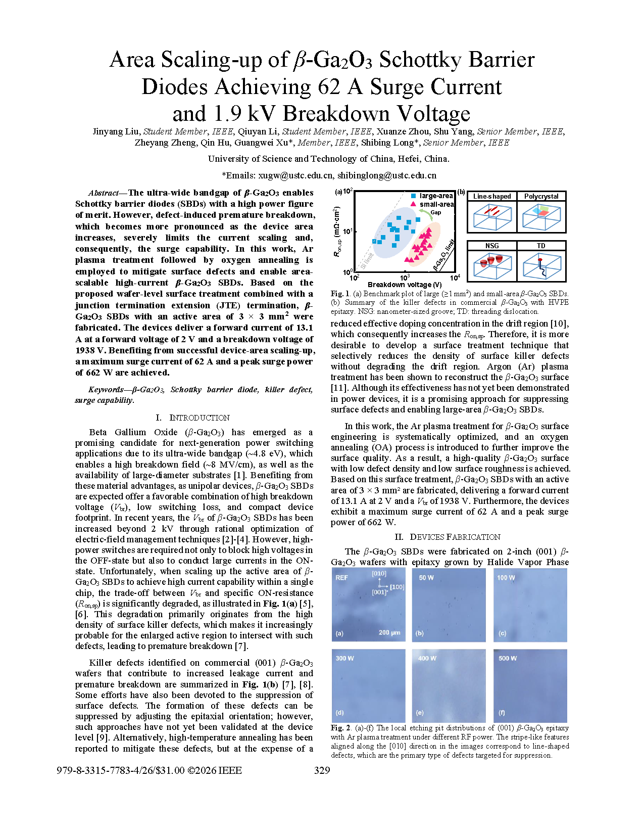
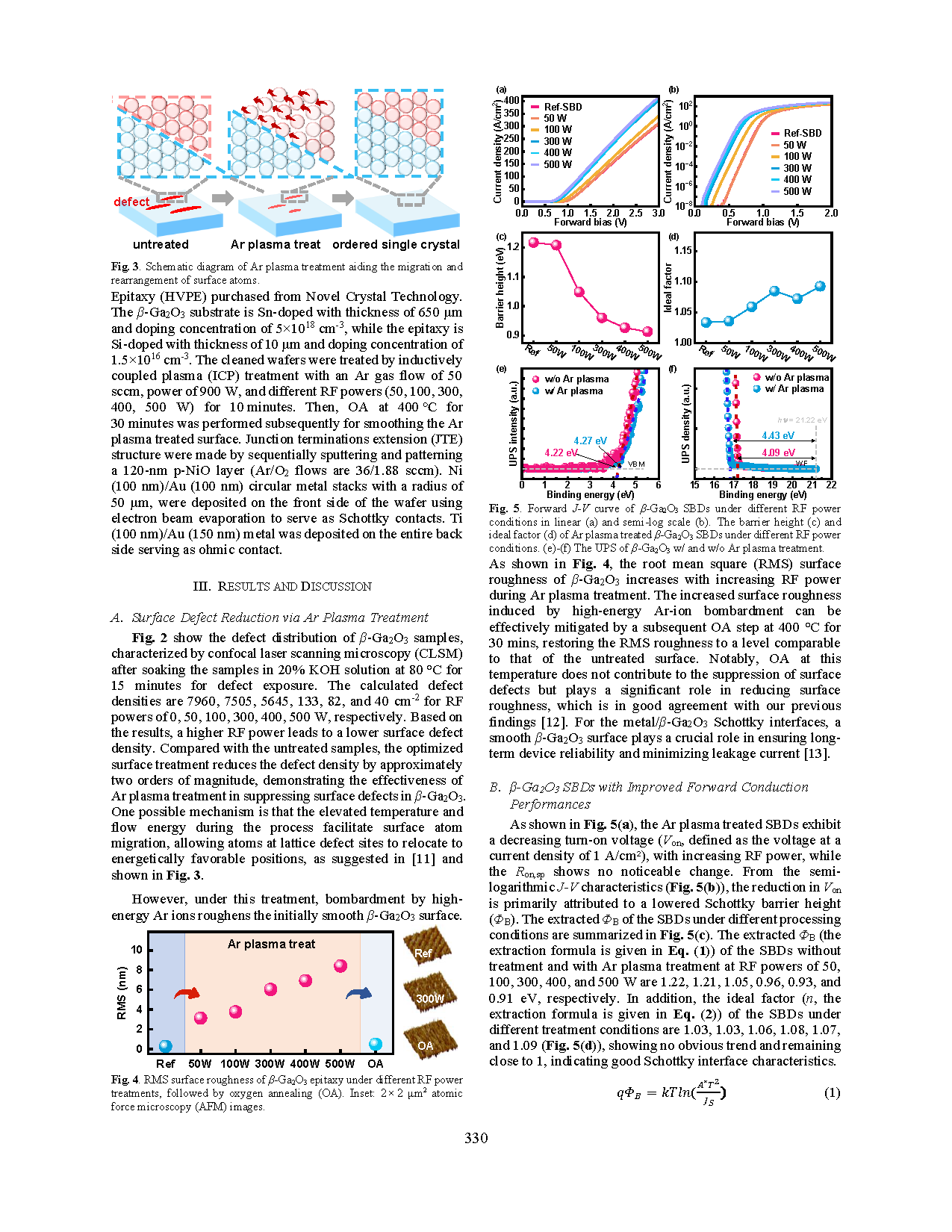
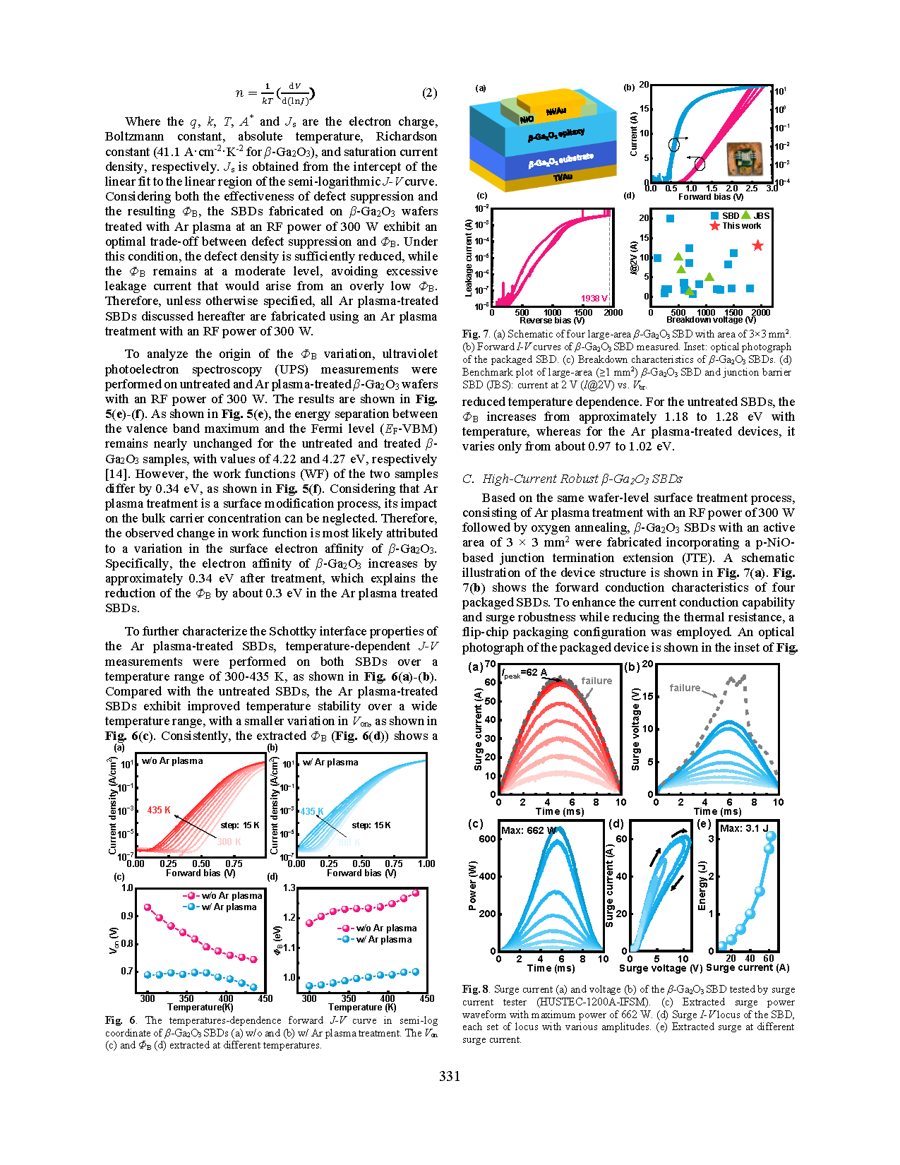
Researchers from the University of Science and Technology of China have published a paper titled " Area Scaling-up of β-Ga₂O₃ Schottky Barrier Diodes Achieving 62 A Surge Current and 1.9 kV Breakdown Voltage " in 2026 IEEE 38th International Symposium on Power Semiconductor Devices and ICs.
Background
Beta Gallium Oxide (β-Ga₂O₃ ) has emerged as a promising candidate for next-generation power switching applications due to its ultra-wide bandgap (~4.8 eV), which enables a high breakdown field (~8 MV/cm), as well as the availability of large-diameter substrates. Benefiting from these material advantages, as unipolar devices, β-Ga₂O₃ SBDs are expected offer a favorable combination of high breakdown voltage (Vbr), low switching loss, and compact device footprint. In recent years, the Vbr of β-Ga₂O₃ SBDs has been increased beyond 2 kV through rational optimization of electric-field management techniques. However, high-power switches are required not only to block high voltages in the OFF-state but also to conduct large currents in the ON-state. Unfortunately, when scaling up the active area of β-Ga₂O₃ SBDs to achieve high current capability within a single chip, the trade-off between Vbr and specific ON-resistance (Ron, sp) is significantly degraded. This degradation primarily originates from the high density of surface killer defects, which makes it increasingly probable for the enlarged active region to intersect with such defects, leading to premature breakdown.
Killer defects identified on commercial (001) β-Ga₂O₃ wafers that contribute to increased leakage current and premature breakdown include line-shaped polycrystal, nanometer-sized groove and threading dislocation. Some efforts have also been devoted to the suppression of surface defects. The formation of these defects can be suppressed by adjusting the epitaxial orientation; however, such approaches have not yet been validated at the device level. Alternatively, high-temperature annealing has been reported to mitigate these defects, but at the expense of a reduced effective doping concentration in the drift region, which consequently increases the Ron, sp. Therefore, it is more desirable to develop a surface treatment technique that selectively reduces the density of surface killer defects without degrading the drift region. Argon (Ar) plasma treatment has been shown to reconstruct the β-Ga₂O₃ surface. Although its effectiveness has not yet been demonstrated in power devices, it is a promising approach for suppressing surface defects and enabling large-area β-Ga₂O₃ SBDs. This work systematically optimizes Ar plasma surface engineering and introduces oxygen annealing to improve surface quality, fabricates 3×3 mm² large-area SBDs with JTE structure, and comprehensively characterizes static, surge and switching performance of the devices.
Abstract
The ultra-wide bandgap of β-Ga₂O₃ enables Schottky barrier diodes (SBDs) with a high power figure of merit. However, defect-induced premature breakdown, which becomes more pronounced as the device area increases, severely limits the current scaling and, consequently, the surge capability. In this work, Ar plasma treatment followed by oxygen annealing is employed to mitigate surface defects and enable area-scalable high-current β-Ga₂O₃ SBDs. Based on the proposed wafer-level surface treatment combined with a junction termination extension (JTE) termination, β-Ga₂O₃ SBDs with an active area of 3 ×3 mm² were fabricated. The devices deliver a forward current of 13.1 A at a forward voltage of 2 V and a breakdown voltage of 1938 V. Benefiting from successful device-area scaling-up, a maximum surge current of 62 A and a peak surge power of 662 W are achieved.
Highlights
A composite wafer-level surface modification process combining Ar plasma treatment and oxygen annealing is proposed, which reduces the surface killer defect density of β-Ga₂O₃ by nearly two orders of magnitude and eliminates premature breakdown during device area scaling-up. Subsequent 400 ℃ oxygen annealing effectively repairs the surface roughness induced by high-energy Ar ion bombardment without degrading the doping concentration of drift region.
The physical mechanism of Schottky barrier height modulation by Ar plasma is revealed: Ar plasma treatment increases the surface electron affinity of β-Ga₂O₃ , reducing the barrier height by up to 0.31 eV and decreasing turn-on voltage. Devices treated by this process exhibit weaker temperature dependence of barrier height and turn-on voltage with superior high-temperature Schottky interface stability.
Large-area β-Ga₂O₃ SBDs with an active area of 3×3 mm² are fabricated with p-NiO based junction termination extension (JTE). The device achieves a forward current of 13.1 A at 2 V and a breakdown voltage of 1938 V, representing state-of-the-art comprehensive performance among reported large-area (≥1 mm²) β-Ga₂O₃ diodes.
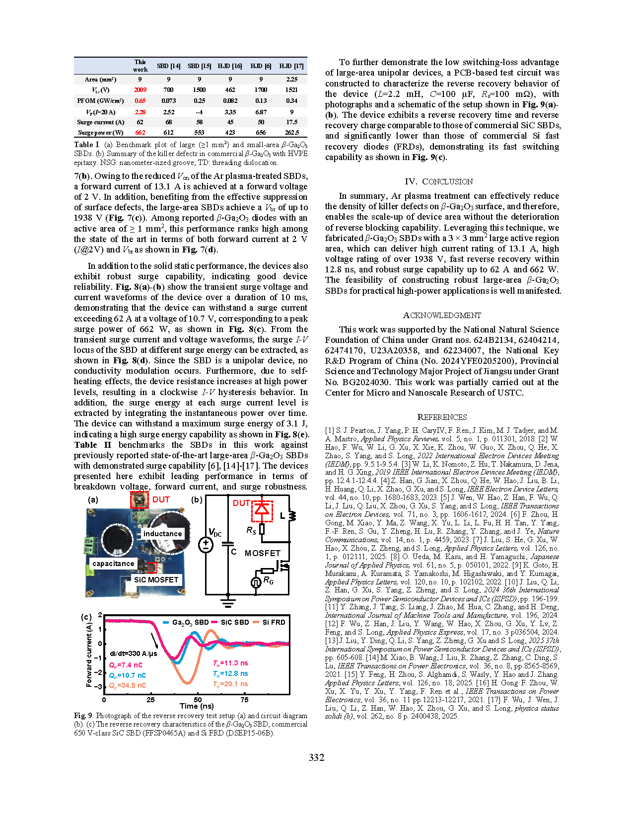
The fabricated devices demonstrate outstanding surge robustness: maximum surge current of 62 A, peak surge power of 662 W and maximum sustainable surge energy of 3.1 J. The reverse recovery performance is comparable with commercial SiC SBDs and far superior to silicon fast recovery diodes (FRDs), featuring ultralow switching loss.
Flip-chip packaging is adopted to reduce thermal resistance, fully verifying the practical application feasibility of monolithic β-Ga₂O₃ power diodes with high voltage, large forward current, robust surge tolerance and ultrafast switching speed for high-power electronic systems.
Conclusion
In summary, Ar plasma treatment can effectively reduce the density of killer defects on β-Ga₂O₃ surface, and therefore, enables the scale-up of device area without the deterioration of reverse blocking capability. Leveraging this technique, we fabricated β-Ga₂O₃ SBDs with a 3 ×3 mm² large active region area, which can deliver high current rating of 13.1 A, high voltage rating of over 1938 V, fast reverse recovery within 12.8 ns, and robust surge capability up to 62 A and 662 W. The feasibility of constructing robust large-area β-Ga₂O₃ SBDs for practical high-power applications is well manifested.
Project Support
This work was supported by the National Natural Science Foundation of China under Grant nos. 624B2134, 62404214, 62474170, U23A20358, and 62234007, the National Key R&D Program of China (No. 2024YFE0205200), Provincial Science and Technology Major Project of Jiangsu under Grant No. BG2024030. This work was partially carried out at the Center for Micro and Nanoscale Research of USTC.
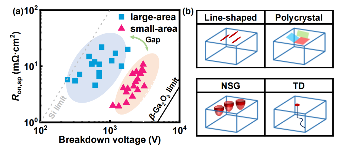
Fig. 1. (a) Benchmark plot of large (≥1 mm²) and small-area β-Ga₂O₃ SBDs. (b) Summary of the killer defects in commercial β-Ga₂O₃ with HVPE epitaxy. NSG: nanometer-sized groove; TD: threading dislocation.
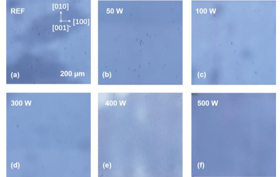
Fig. 2. (a)-(f) The local etching pit distributions of (001) β-Ga₂O₃ epitaxy with Ar plasma treatment under different RF power. The stripe-like features aligned along the [010] direction in the images correspond to line-shaped defects, which are the primary type of defects targeted for suppression.
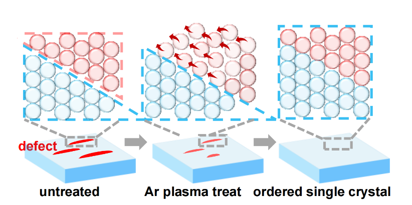
Fig. 3. Schematic diagram of Ar plasma treatment aiding the migration and rearrangement of surface atoms.
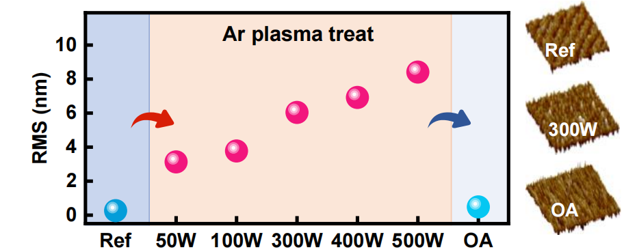
Fig. 4. RMS surface roughness of β-Ga₂O₃ epitaxy under different RF power treatments, followed by oxygen annealing (OA). Inset: 2 × 2 μm² atomic force microscopy (AFM) images.
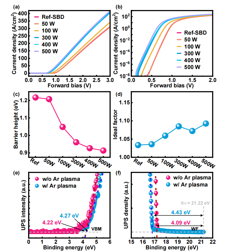
Fig. 5. Forward J-V curve of β-Ga₂O₃ SBDs under different RF power conditions in linear (a) and semi-log scale (b). The barrier height (c) and ideal factor (d) of Ar plasma treated β-Ga₂O₃ SBDs under different RF power conditions. (e)-(f) The UPS of β-Ga₂O₃ w/and w/o Ar plasma treatment.
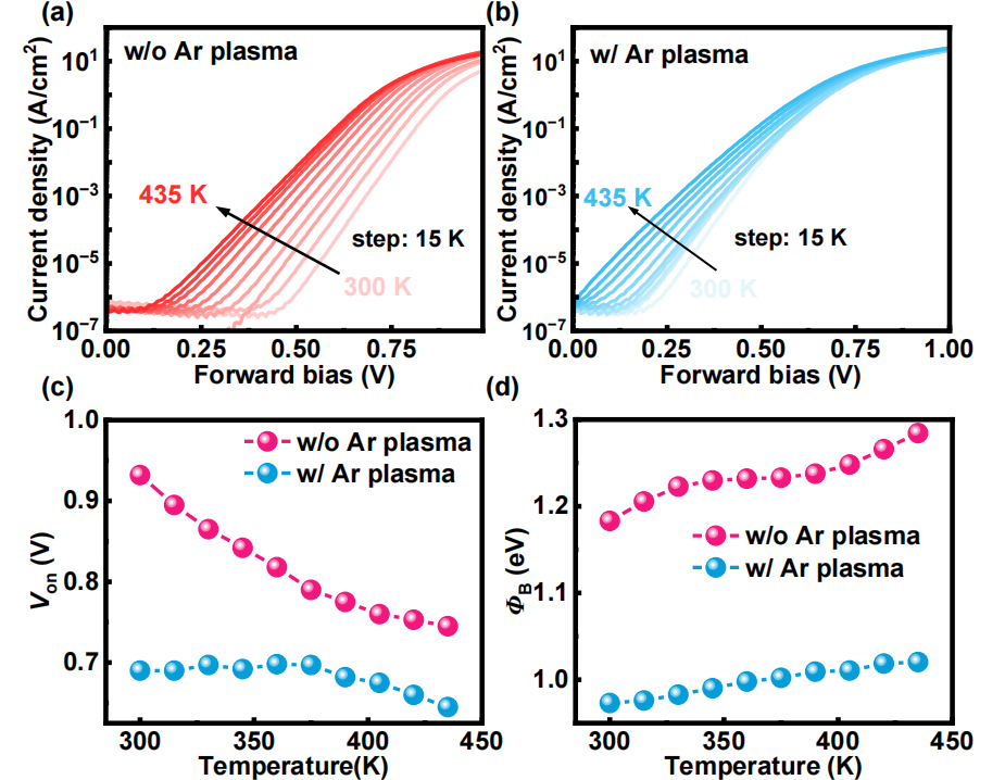
Fig. 6. The temperatures-dependence forward J-V curve in semi-log coordinate of β-Ga₂O₃ SBDs (a) w/o and (b) w/ Ar plasma treatment. The Von (c) and ΦB (d) extracted at different temperatures.
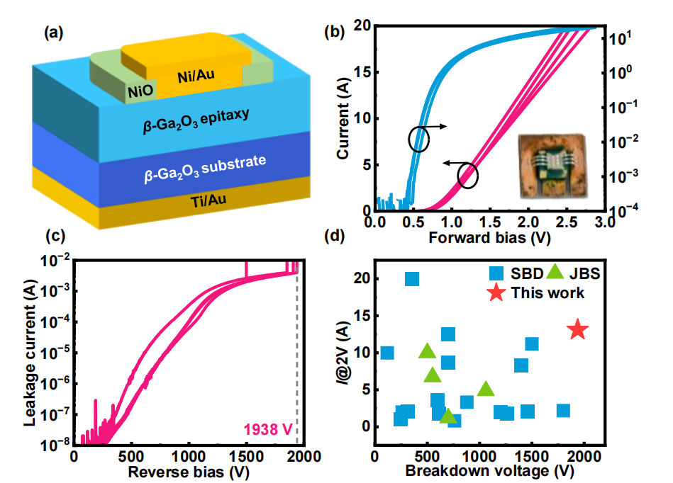
Fig. 7. (a) Schematic of large-area β-Ga₂O₃ SBD with area of 3×3 mm². (b) Forward I-V curves of the packaged SBD. Inset: optical photograph of the packaged SBD. (c) Breakdown characteristics of β-Ga₂O₃ SBDs. (d) Benchmark plot of large-area (≥1 mm²) β-Ga₂O₃ SBD and junction barrier SBD (JBS): current at 2 V (I@2V) vs. Vbr.
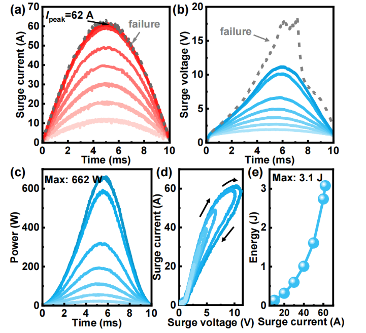
Fig. 8. Surge current (a) and voltage (b) of the β-Ga₂O₃ SBD tested by surge current tester (HUSTEC-1200A-IFSM). (c) Extracted surge power at different waveform with maximum power of 662 W. (d) Surge I-V locus of the SBD, each set of locus with various amplitudes. (e) Extracted surge energy.
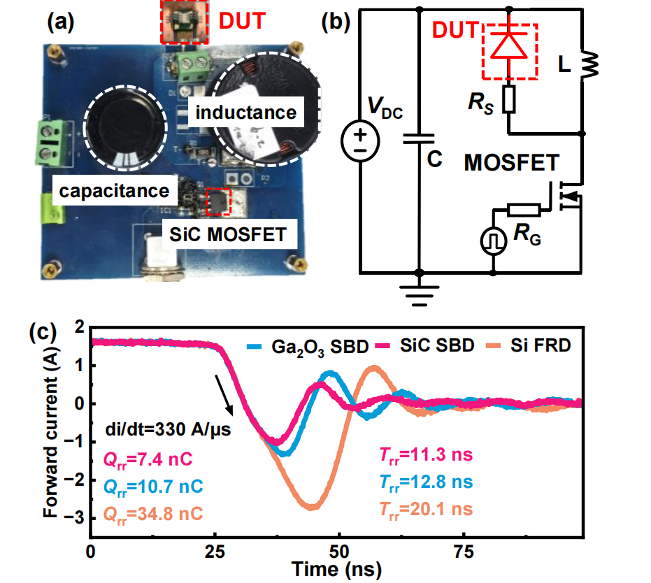
Fig. 9. Photograph of the reverse recovery test setup (a) and circuit diagram (b). (c) The reverse recovery characteristics of the β-Ga₂O₃ SBD, commercial 650 V-class SiC SBD (FFSP0465A) and Si FRD (DSEP15-06B).
DOI :
10.1109/ISPSD64561.2026.11553647
Instruction
Official Account

Cooperation
Top
