


The research team led by Professor Xin Ke Liu from Shenzhen University has published a paper titled He-induced semi-insulating microcolumns for high-voltage leakage current suppression in β-Ga₂O₃ Schottky barrier diodes in the academic journal Applied Physics Letters.
Background
β-Ga₂O₃ features an ultra-wide bandgap of 4.8–4.9 eV and a theoretical breakdown electric field of 8 MV/cm, making it a highly competitive candidate for next-generation high-voltage power electronic devices. Schottky barrier diodes (SBDs), with their simple structure, low conduction losses, and fast switching speed, are among the key device architectures for Ga₂O₃ power electronics.
However, conventional β-Ga₂O₃ SBDs can exhibit significant reverse leakage current under high reverse bias due to effects such as Schottky barrier lowering, which limits their breakdown voltage and practical engineering applications. Various approaches have been explored to improve the leakage characteristics of Ga₂O₃ devices, including epitaxial growth and device-structure optimization. Although reducing the carrier concentration in the drift layer can improve reverse-bias characteristics to some extent, it increases the difficulty of epitaxial growth and simultaneously degrades forward conduction performance.
Junction barrier Schottky (JBS) diodes and trench MOS/MIS devices can suppress leakage current by modulating the electric field through charge coupling and the RESURF effect. However, JBS structures are constrained by the lack of stable p-type doping in β-Ga₂O₃, while trench-based devices involve relatively complex fabrication processes and higher manufacturing costs.
Therefore, developing an SBD architecture that can effectively suppress high-voltage reverse leakage current while maintaining a simple fabrication process remains a key challenge in the field of Ga₂O₃ power electronics. In this work, the researchers propose a semi-insulating microcolumn-based SIMC-SBD architecture constructed through helium-ion implantation. The approach achieves low leakage current under high reverse bias without significantly increasing process complexity, addressing a gap in this particular device-engineering approach.
Abstract
Local semi-insulating regions in β-Ga₂O₃ are critical for high-voltage devices, as they can regulate the interfacial electric field and improve leakage-current characteristics. The research team introduced a high concentration of acceptor-like defects into the n⁻-Ga₂O₃ matrix through helium-ion implantation, thereby forming an array of semi-insulating microcolumns in situ. These semi-insulating microcolumns effectively reduce the electric field near the Schottky junction, decrease the effective anode area in direct metal–semiconductor contact, and significantly suppress reverse leakage current.
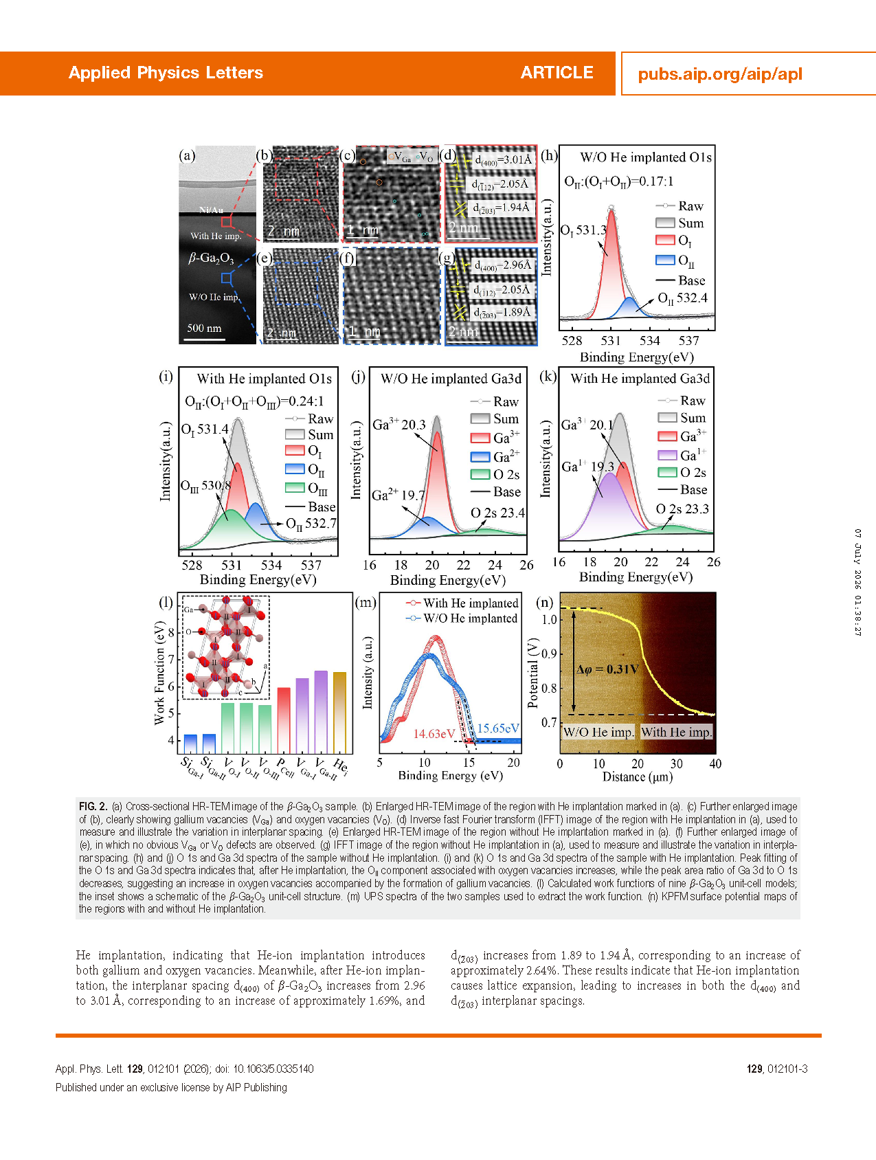
Through a combination of SRIM simulations, HR-TEM, XPS, UPS, and KPFM characterization, the researchers confirmed that He-ion implantation generates a large number of acceptor-like defects, including gallium vacancies (VGa) and interstitial helium atoms (Heᵢ). These defects compensate for free carriers and locally transform n⁻-Ga₂O₃ into a semi-insulating state, substantially reducing the electrical conductivity of the implanted Ga₂O₃ regions.
In the fabricated Ga₂O₃ SIMC-SBD, the semi-insulating microcolumns occupied 28% of the total anode area. At a reverse bias of 1000 V, the reverse leakage current was reduced by nearly two orders of magnitude compared with that of a conventional SBD, while the device achieved a breakdown voltage of up to 1807 V. This architecture provides a simple and feasible approach for developing β-Ga₂O₃ SBDs that simultaneously achieve high breakdown voltage and low leakage current.
Highlights
In-situ formation of semi-insulating microcolumn arrays: Helium-ion implantation is used to form semi-insulating microcolumn arrays in β-Ga₂O₃, dominated by acceptor-like defects such as VGa and Heᵢ, enabling localized conversion to a semi-insulating state. Multiscale characterization confirms that He-ion implantation increases the material work function and induces carrier compensation, revealing the evolution mechanism of implantation-induced defects.
Significant suppression of reverse leakage current: Under a reverse bias of 1000 V, the SIMC-SBD achieves a reverse leakage current approximately two orders of magnitude lower than that of a conventional SBD, while maintaining a breakdown voltage of 1807 V.
Clarification of the leakage-suppression mechanism: The semi-insulating microcolumns reshape the interfacial electric-field distribution and reduce the peak electric field near the interface. Meanwhile, they reduce the effective metal–semiconductor contact area of the anode, thereby limiting leakage-current pathways. The study elucidates the underlying mechanism responsible for leakage-current suppression.
Conclusion
By introducing a high density of acceptor-like VGa and Heᵢ defects into Ga₂O₃ through helium-ion implantation, the researchers achieved the in-situ formation of semi-insulating microcolumns beneath the Schottky anode. These semi-insulating microcolumns suppress high-voltage reverse leakage current through two synergistic mechanisms: they modulate the electric-field distribution near the Schottky junction and reduce the interfacial electric field, while simultaneously reducing the effective metal–semiconductor contact area, thereby limiting leakage-current pathways.
The fabricated SIMC-SBD achieved a breakdown voltage of 1807 V and a specific on-resistance of 4.1 mΩ·cm². At a reverse voltage of 1000 V, its leakage current was reduced by nearly two orders of magnitude compared with that of a conventional SBD, significantly lowering the off-state power consumption.
This defect-engineering-induced local semi-insulating strategy provides a new design approach for high-voltage β-Ga₂O₃ Schottky power devices.
Project Support
This work was supported by the National Key Research and Development Program of China (2024YFE0205100), the Major Project of Guangdong Basic and Applied Basic Research Foundation (2023B0303000012), the Shenzhen Science and Technology Program (SGDX20240115101802004), the Shenzhen University Scientific Instrument Development Project (2024YQ003), and the Independent Research Project of the State Key Laboratory of Radio Frequency Heterogeneous Integration (2025007).
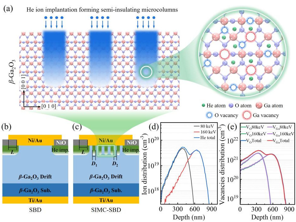
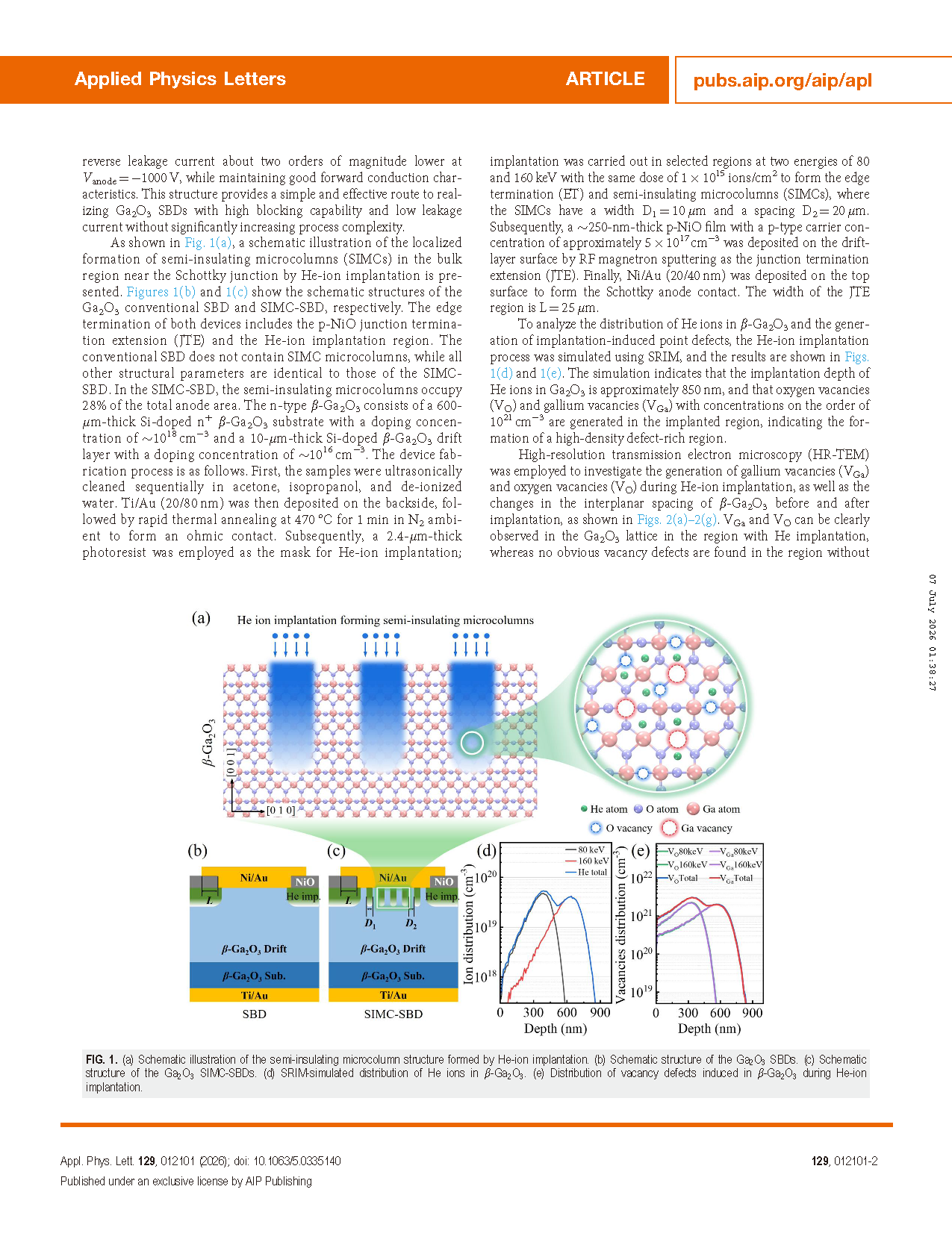
FIG 1 (a) Schematic illustration of the semi-insulating microcolumn structure formed by He-ion implantation; (b) schematic illustration of the conventional Ga₂O₃ SBD device structure; (c) schematic illustration of the SIMC-SBD device structure; (d) SRIM-simulated distribution of He ions inside Ga₂O₃; (e) distribution of vacancy defects induced by He-ion implantation.
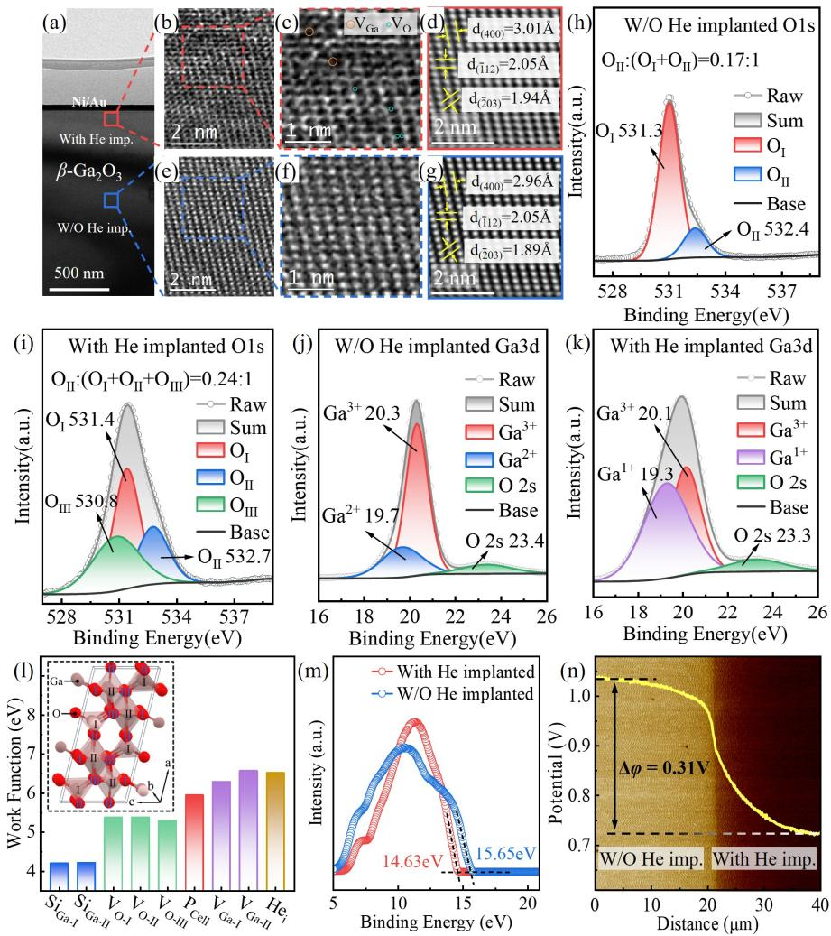
FIG 2 (a) Cross-sectional HR-TEM image of β-Ga₂O₃; (b–g) HR-TEM images and IFFT analyses of regions with and without He implantation; (h–k) XPS spectra of O 1s and Ga 3d for samples with and without He implantation; (l) work functions of different defect models; (m) comparison of work functions obtained from UPS measurements; (n) KPFM surface-potential measurement results.
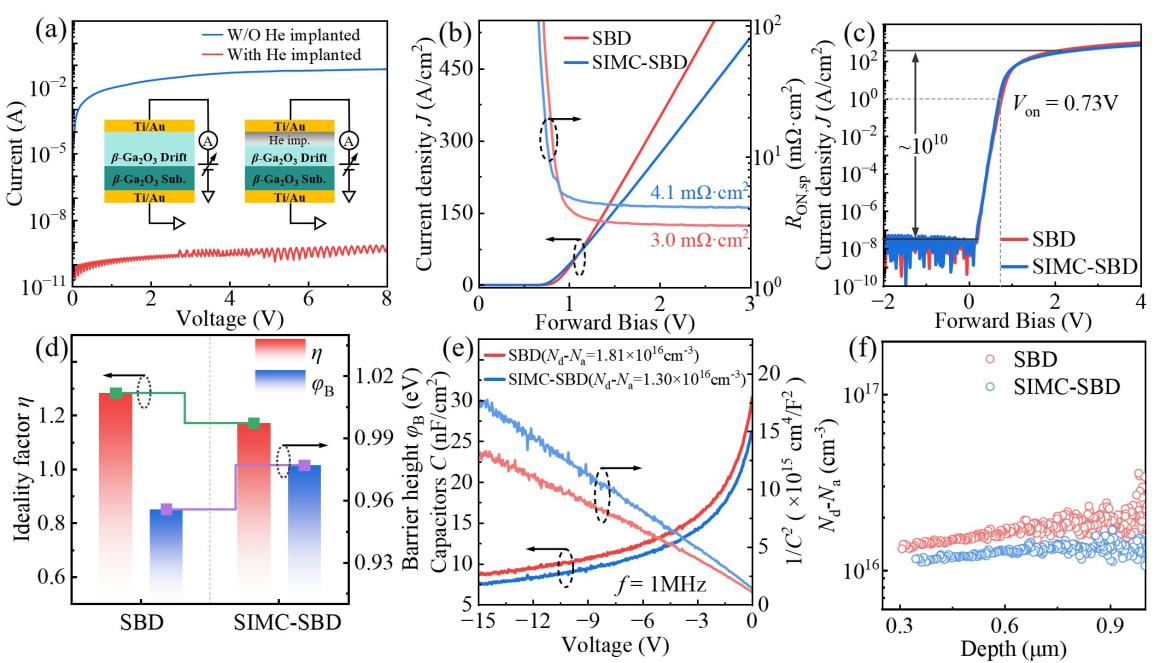
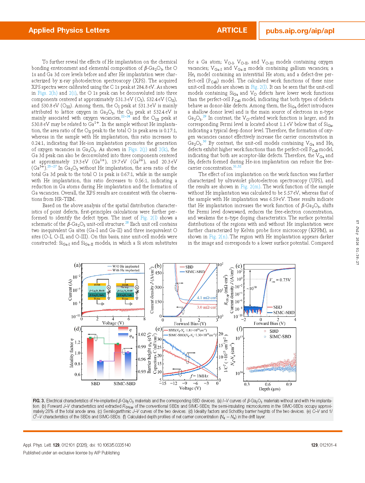
FIG 3 (a) I–V characteristics of Ga₂O₃ material layers with and without He implantation; (b) forward J–V characteristics and specific on-resistance of conventional SBD and SIMC-SBD devices; (c) J–V curves of the two devices plotted on a semilogarithmic scale; (d) ideality factor and Schottky barrier height; (e) C–V and 1/C²–V measurement curves; (f) depth profiles of the net carrier concentration in the drift layer.
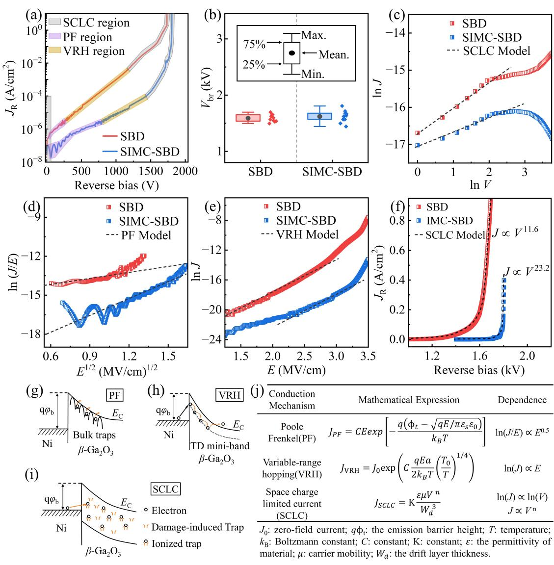
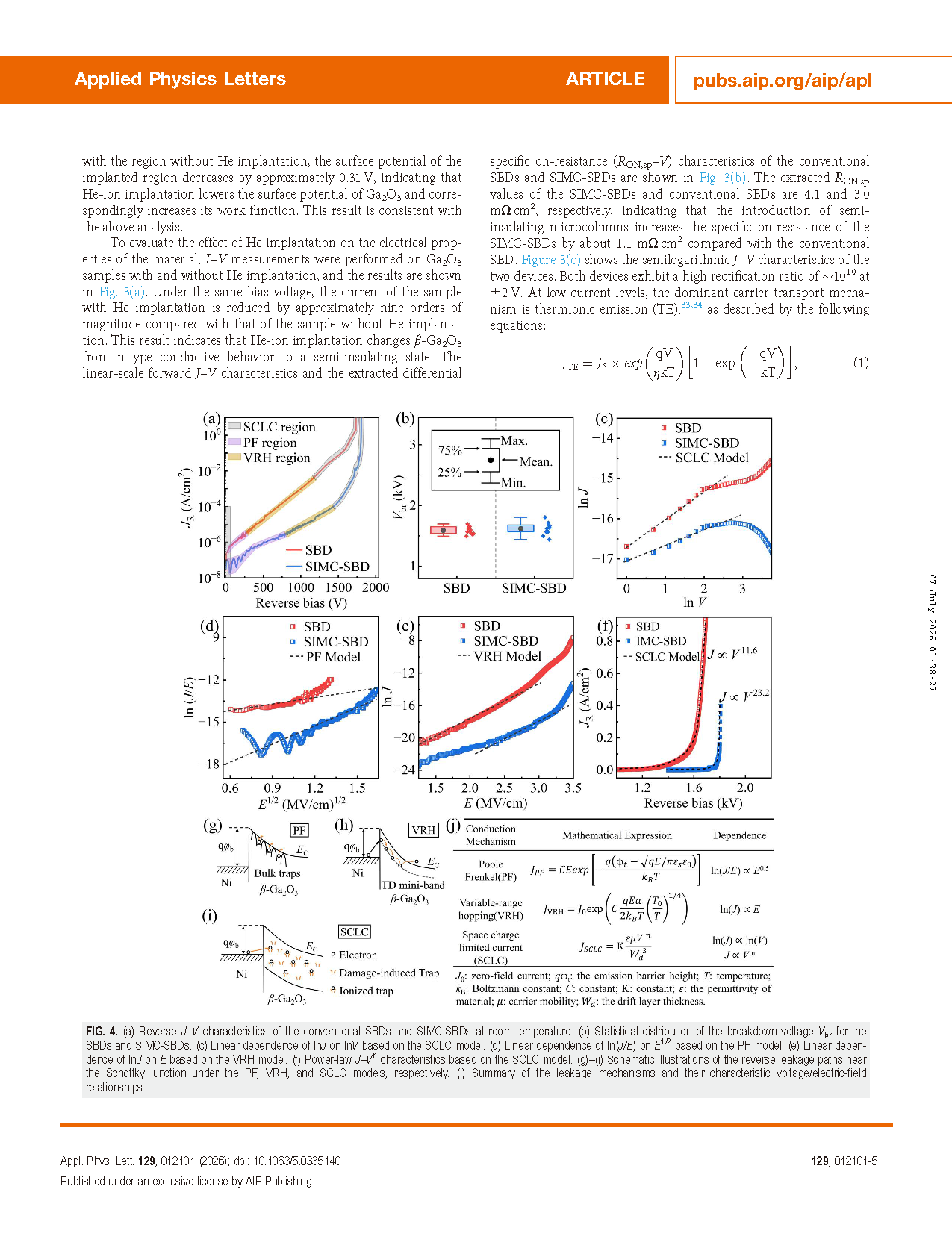
FIG 4 (a) Reverse J–V characteristics of the two types of devices at room temperature; (b) statistical distribution of the breakdown voltage; (c–f) fitting analyses based on the SCLC, PF, and VRH leakage-transport models; (g–i) schematic illustrations of the PF, VRH, and SCLC leakage-transport pathways; (j) summary of the characteristic relationships among different leakage mechanisms.
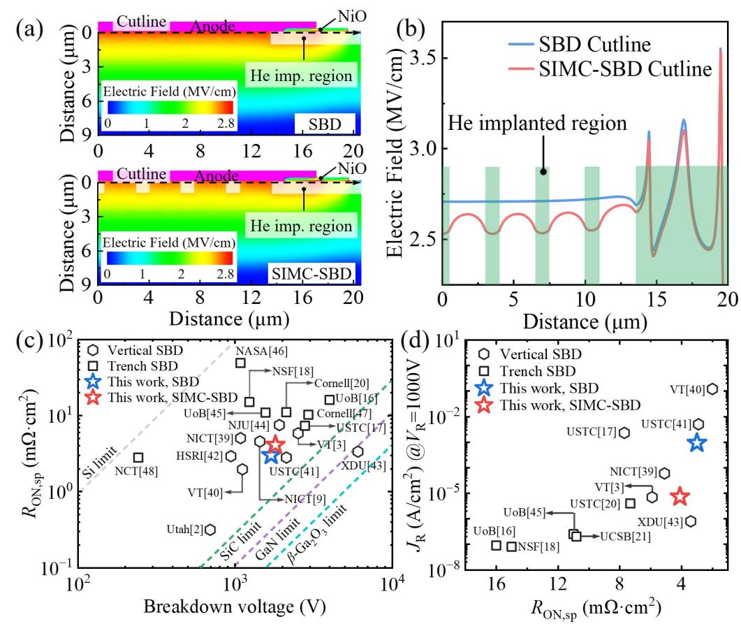
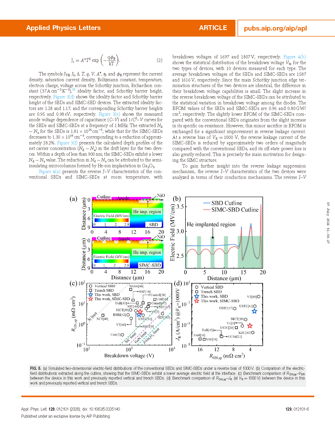
FIG 5 (a) TCAD-simulated electric-field distribution at a reverse voltage of Vᵣ = 1000 V; (b) comparison of the electric-field distributions along the device cross-sectional cutline; (c) comparison of Rₒₙ,ₛₚ–Vᴮᴿ performance with previously reported vertical/trench SBDs; (d) comparison of Rₒₙ,ₛₚ–Jᵣ (Vᵣ = 1000 V) performance with previously reported devices.
Team Introduction
Xin Ke Liu is a National Young Talent (2025), Principal Scientist of the National Key Research and Development Program of China (2025), a Fellow of the Institute of Physics (FInstP, 2025), a Fellow of the Royal Society of Chemistry (FRSC, 2024), and a doctoral supervisor.
He received his Bachelor’s degree with Honors in Materials Science from the National University of Singapore in 2008, his Ph.D. in Microelectronics from the Department of Electrical and Computer Engineering at the National University of Singapore in 2013, and a Certificate in Technology Management from the National University of Singapore in 2010.
Professor Liu currently serves as Director of the Institute of Power Semiconductor Devices and AI Energy Monitoring Engineering Technology at Shenzhen University, and as a Distinguished Professor of the College of Materials Science and Engineering and the State Key Laboratory of Radio Frequency Heterogeneous Integration.
He has long been engaged in research on wide-bandgap semiconductor GaN materials and devices. As a first or corresponding author, he has published 131 SCI-indexed papers in international journals including Materials Today, Advanced Materials, IEEE Electron Device Letters (IEEE EDL), and IEEE Transactions on Electron Devices (IEEE TED). He has also authored the books Gallium Nitride Single-Crystal Materials and Devices and Science and Technology Archaeology and Cultural Relic Appreciation.
Professor Liu has led major research projects funded by the National Key Research and Development Program of China, the National Natural Science Foundation of China (Young Scientists Fund and General Program), and the Guangdong Provincial Natural Science Foundation Distinguished Young Scholars Program, among others.
As the primary award recipient or individual recipient, he has received the Bronze Award in the 2021 Guangdong Universities Science and Technology Achievement Transformation Finals, the Second Prize of the 2022 Guangdong Science and Technology Progress Award, the Second Prize of the 2022 China Electronics Society Science and Technology Progress Award, the Second Prize of the 2022 Guangdong Electronics Society Science and Technology Progress Award, the 2023 Shenzhen Youth Science and Technology Award, and the 2025 Guangdong Youth Science and Technology Award.
DOI:
10.1063/5.0335140
Instruction
Official Account

Cooperation
Top
