


With the rapid evolution of the wide‑bandgap semiconductor industry, technologies based on third‑generation gallium nitride (GaN) and fourth‑generation gallium oxide (Ga₂O₃) materials continue to advance, with broad applications in high‑voltage power, RF, optoelectronics, and other key fields. Among them, advanced crystal‑growth and epitaxy equipment serves as the critical foundation for the localization of the semiconductor industry, directly determining the efficiency of material development and mass production and representing an essential requirement for the continued growth of the sector.
In high‑voltage Ga₂O₃ power devices, the epitaxial layer serves as the key drift region and directly withstands the applied voltage. The device breakdown voltage is strongly correlated with the thickness of the epitaxial layer. For 10‑kV‑class ultra‑high‑voltage devices, epitaxial layers with thicknesses of several tens of micrometers are required to meet practical operating conditions.
Conventional MOCVD processes are better suited to precision growth of thin epitaxial layers, with typical growth rates of only 1–2 μm/h. Their extremely low efficiency and high production cost for thick‑film epitaxy make them difficult to apply to the large‑scale manufacturing of high‑voltage Ga₂O₃ devices. In contrast, hydride vapor phase epitaxy (HVPE) offers significant advantages. With growth rates an order of magnitude higher, excellent thick‑film uniformity, and strong production stability, HVPE has emerged as a leading technology for the fabrication of thick Ga₂O₃ epitaxial layers.
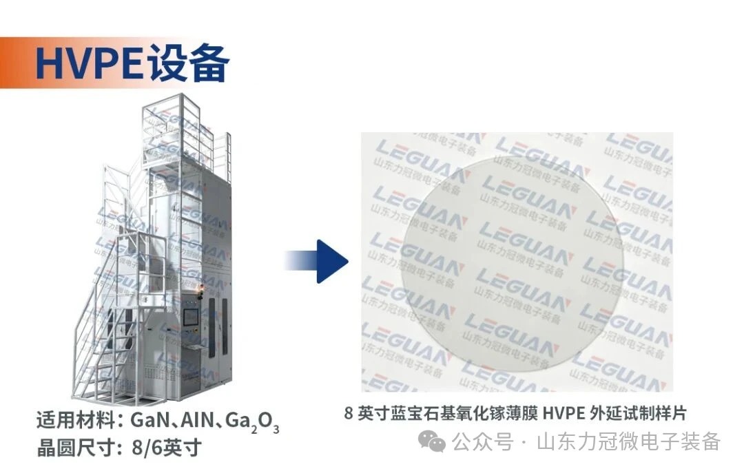
Drawing on its profound in-house R&D heritage in semiconductor equipment, Shandong Liguang has independently developed the 8-inch HVPE epitaxy equipment. The equipment has completed full-process testing and process validation in the company’s in-house professional HVPE laboratory. It delivers stable overall operation and outstanding performance and is now fully available on the market. The company has built a dedicated PhD-level process team focused on R&D, optimization and process tuning of HVPE equipment. Equipped with an advanced 8-inch HVPE process laboratory, it can provide customers with comprehensive supporting services including tool testing, process verification and technical commissioning, helping customers carry out R&D work with high efficiency.
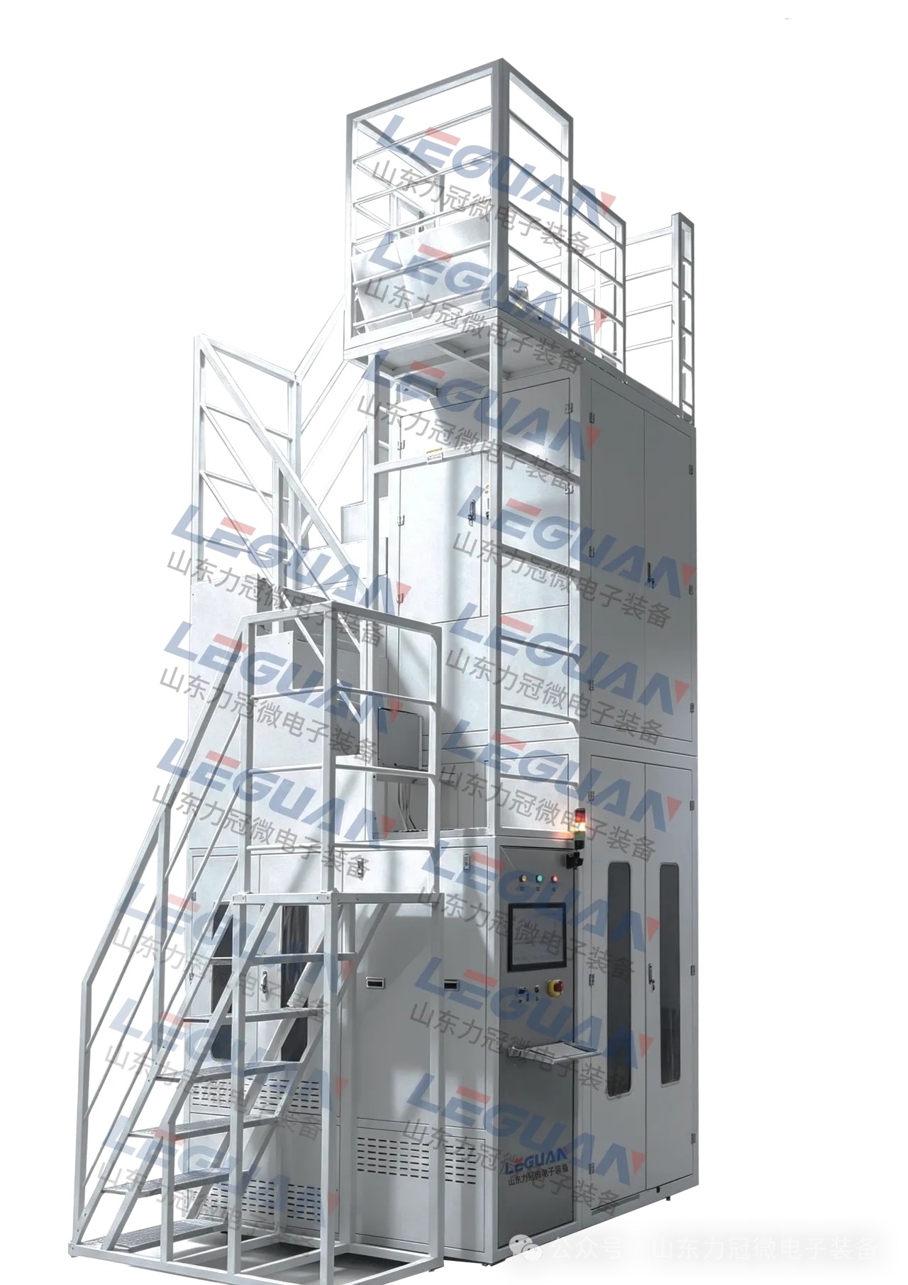
8-Inch HVPE Equipment
Drawing on solid R&D strength and accumulated process know-how, the company has secured key technological breakthroughs in 8-inch gallium oxide HVPE epitaxy. Its R&D team performed dedicated process validation on 8-inch sapphire substrates and realized high-quality gallium oxide heteroepitaxial growth with outstanding key process indicators:
Epitaxial film thickness of over 20 μm, fully satisfying the fabrication requirements for thick drift layers of 10-kV-class high-voltage devices;
Thickness uniformity (maximum deviation) better than 20%; the optimal batches achieve non-uniformity below 5%, with performance on par with mature 4-inch HVPE mass-production equipment;
Sustained stable growth rates of 10-20 μm/h, with mass-production efficiency far exceeding that of conventional MOCVD processes;
Favorable surface-morphology uniformity over the entire 8-inch substrate, with remarkable controllability of epitaxial growth and excellent batch-to-batch consistency.
The successful 8‑inch large‑size process validation effectively tackles industry pain points of poor uniformity and inadequate stability for large‑size thick‑film epitaxy. It builds a solid equipment‑and‑technology foundation for gallium oxide power devices to evolve toward larger wafer dimensions, higher withstand‑voltage ratings and large‑scale mass production.
Unlike single‑function epitaxy equipment, our 8‑inch HVPE equipment features excellent process compatibility and wide industrial versatility, truly realizing dual‑function capability and empowering two technical tracks. The equipment can stably achieve high‑quality thick‑film gallium oxide epitaxy for R&D and mass production of high‑voltage power devices, and can also meet the requirements for gallium nitride crystal growth to accommodate diverse R&D scenarios.
Shandong Liguang has long focused on the R&D and manufacturing of high‑end semiconductor equipment. It builds superior equipment with professionalism and continuously creates value for customers with ingenuity.
Instruction
Official Account

Cooperation
Top
