


Researchers from the Xidian University have published a dissertation titled " Van der Waals epitaxy of β-Ga₂O₃ films on polycrystalline diamond substrates enabled by graphene interlayer for efficient thermal management " in Diamond and Related Materials.
Background
Gallium oxide (Ga₂O₃), an ultra-wide-bandgap semiconductor with a bandgap of 4.9-5.3 eV, possesses outstanding breakdown field strength, low energy loss and excellent thermal & chemical stability. Its Baliga’s figure of merit is 4 times that of GaN and 10 times that of SiC, making it a prime candidate for next-generation high-power electronics and solar-blind optoelectronic devices. Nevertheless, intrinsic β-Ga₂O₃ only delivers thermal conductivity of 10-30 W·m⁻¹·K⁻¹. Severe self-heating emerges during device miniaturization and power scaling, which severely degrades device reliability and becomes a core bottleneck restricting practical deployment.
Diamond exhibits the highest thermal conductivity (~2000 W·m⁻¹·K⁻¹) among all natural materials, serving as an ideal heat-spreading substrate. Existing studies mostly realize Ga₂O₃ epitaxy on single-crystal diamond, yet large-area single-crystal diamond suffers from extremely high cost and poor scalability. Polycrystalline diamond is low-cost and available in large sizes, but random crystallographic orientations of its grains trigger severe lattice mismatch and huge interfacial thermal stress during direct heteroepitaxy of Ga₂O₃, leading to cracked films and poor crystallinity.
Traditional heterogeneous integration technologies including surface-activated bonding and ion-lift transfer inevitably introduce irradiation-induced defects and amorphous interlayers, accompanied by complicated fabrication procedures and high interfacial thermal resistance. Two-dimensional materials (graphene, hexagonal boron nitride h-BN) feature dangling-bond-free van der Waals interfaces and hexagonal atomic arrangements, capable of alleviating lattice and thermal mismatch. To date, no systematic research has reported van der Waals epitaxy of high-quality phase-pure β-Ga₂O₃ on polycrystalline diamond via single-layer graphene interlayer. In this work, mist chemical vapor deposition (mist-CVD) is adopted with monolayer graphene interlayer to tackle the above fundamental challenges, and the heat dissipation performance as well as optoelectronic device performance are comprehensively verified.
Abstract
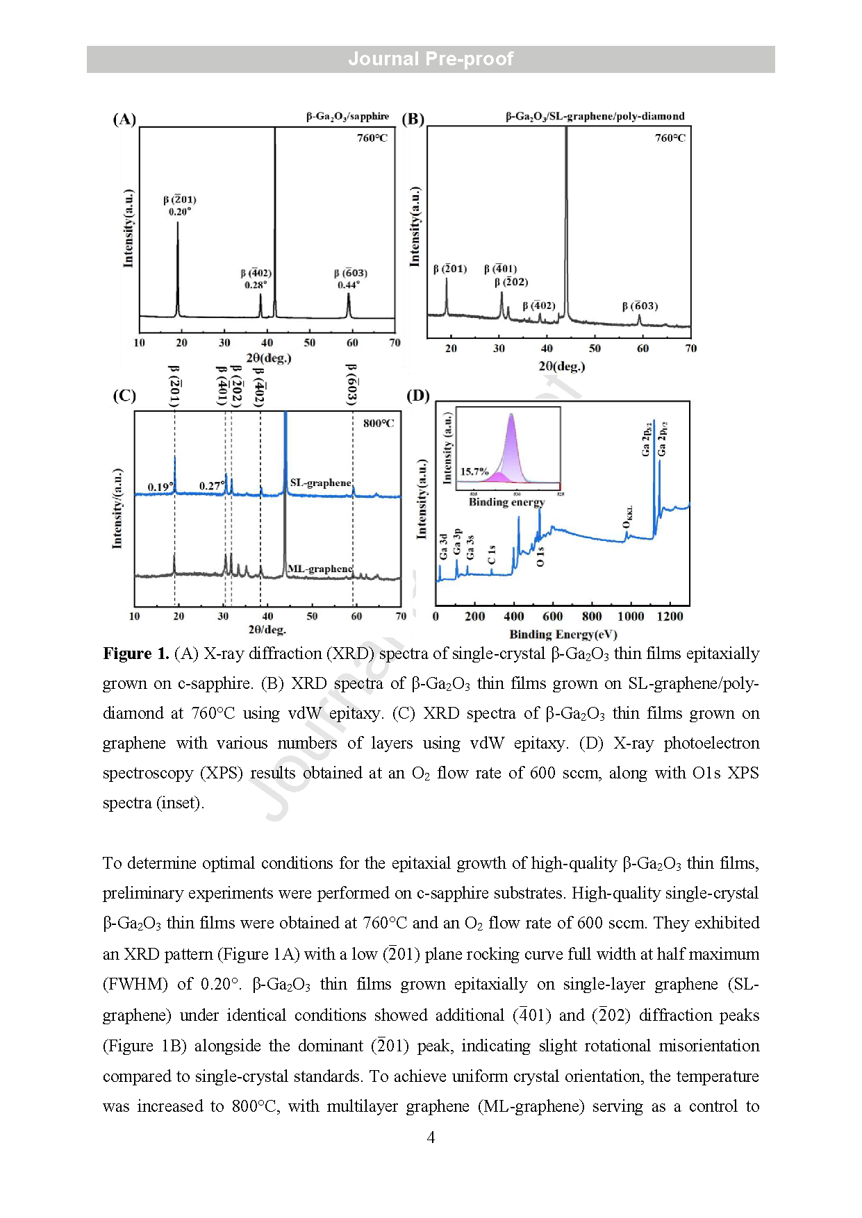
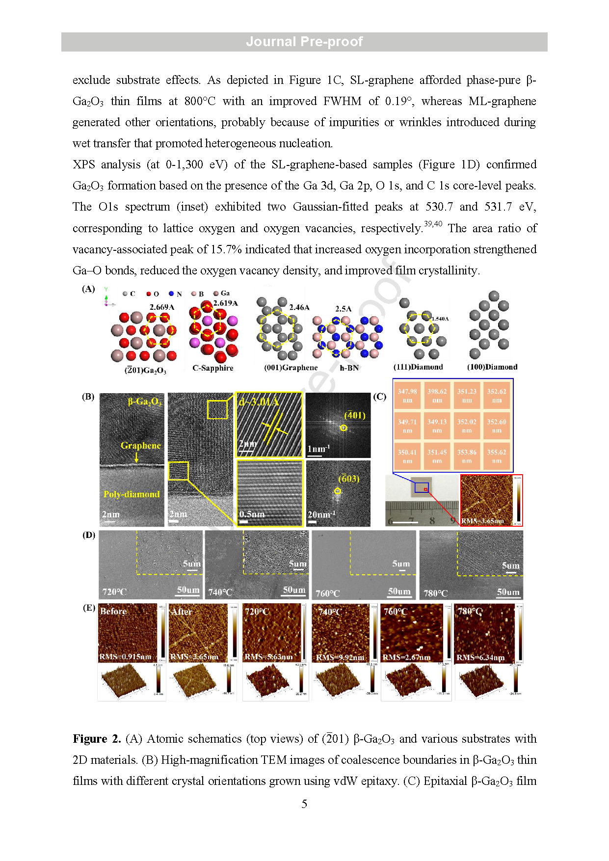
Heteroepitaxy of β-Ga₂O₃ on polycrystalline diamond provides a critical thermal management solution for high-power devices but is hindered by the disordered crystallographic orientations of the substrate. In this research, a graphene interlayer is used to mitigate lattice mismatch and interfacial thermal stress, enhancing film quality. Results reveal that the thin-film growth follows the Stranski-Krastanov mode and the produced β-Ga₂O₃ films exhibit preferential growth along the (2̅01) plane, with an average surface roughness of 3.65 nm and a full width at half maximum as narrow as 0.19°, confirming the successful epitaxy of high-crystallinity, phase-pure β-Ga₂O₃ thin films. Infrared thermography confirms the superior heat dissipation capability of the diamond substrate, yielding an external effective thermal conductivity of 95.8 W/m·K. A fabricated β-Ga₂O₃-based photodetector exhibits a dark current of 1.2 nA, photo-to-dark current ratio of 10⁵, and responsivity of 218 A/W. This study overcomes the fundamental challenge of the epitaxy of Ga₂O₃ on diamond, advancing next-generation highpower and optoelectronic semiconductor technologies.
Highlights
Single-layer graphene enables van der Waals epitaxy of β-Ga₂O₃ on polycrystalline diamond.
The graphene interlayer reduces lattice mismatch and relieves interfacial thermal stress.
β-Ga₂O₃ films show high crystallinity (FWHM 0.19°) and low roughness (3.65 nm RMS).
Diamond substrate yields external effective thermal conductivity of 95.8 W/m·K.
β-Ga₂O₃ photodetector on diamond exhibits high responsivity (218 A/W) and PDCR (10⁵).
Conclusion
This study demonstrates the first successful epitaxial growth of high-quality, phase-pure β-Ga₂O₃ thin films on polycrystalline diamond substrates via mist-CVD, achieved through the strategic use of a single-layer graphene interlayer. The graphene effectively mitigates lattice mismatch and relieves interfacial thermal stress arising from the disordered substrate orientation. The resulting films exhibit preferential growth along the (2̅01) plane, alongside minor (4̅01) and (2̅02) orientations, with a narrow rocking curve FWHM of 0.19° and a low RMS roughness of 3.65 nm. Detailed analysis reveals that the film growth follows the Stranski-Krastanov mode, with mixed-type dislocations forming during island coalescence due to nonuniform nucleation sites. The graphene interlayer plays a critical role in buffering thermal stress, preventing delamination, and ensuring film continuity. Infrared thermography confirms the superior heat dissipation capability of the diamond substrate, yielding an external effective thermal conductivity of 95.8 W/m·K—more than three times that of pristine β-Ga₂O₃. A photodetector fabricated on this heterostructure exhibits excellent performance, including a dark current of 1.2 nA, a photo-to-dark current ratio of 10⁵, and a responsivity of 218 A/W. These findings overcome the longstanding challenge of direct β-Ga₂O₃ epitaxy on diamond, establishing a robust platform for next-generation high-power and optoelectronic devices with integrated thermal management.
Project Support
This work was supported by The Fundamental and Interdisciplinary Disciplines Breakthrough Plan of the Ministry of Education of China (Grant No. JYB2025XDXM105); The General Program of Natural Science Foundation of China (Grant No: 62274134, 62421005); The National Science Fund for Distinguished Young Scholars (Grant No: 62525402); The National Key Research and Development Program (Grant Nos: 2023YFB3609900 and 2021YFA0716400) and the Natural Science Basic Research Program of Shaanxi Province (Grant No. 2025SYS-SYSZD-084).
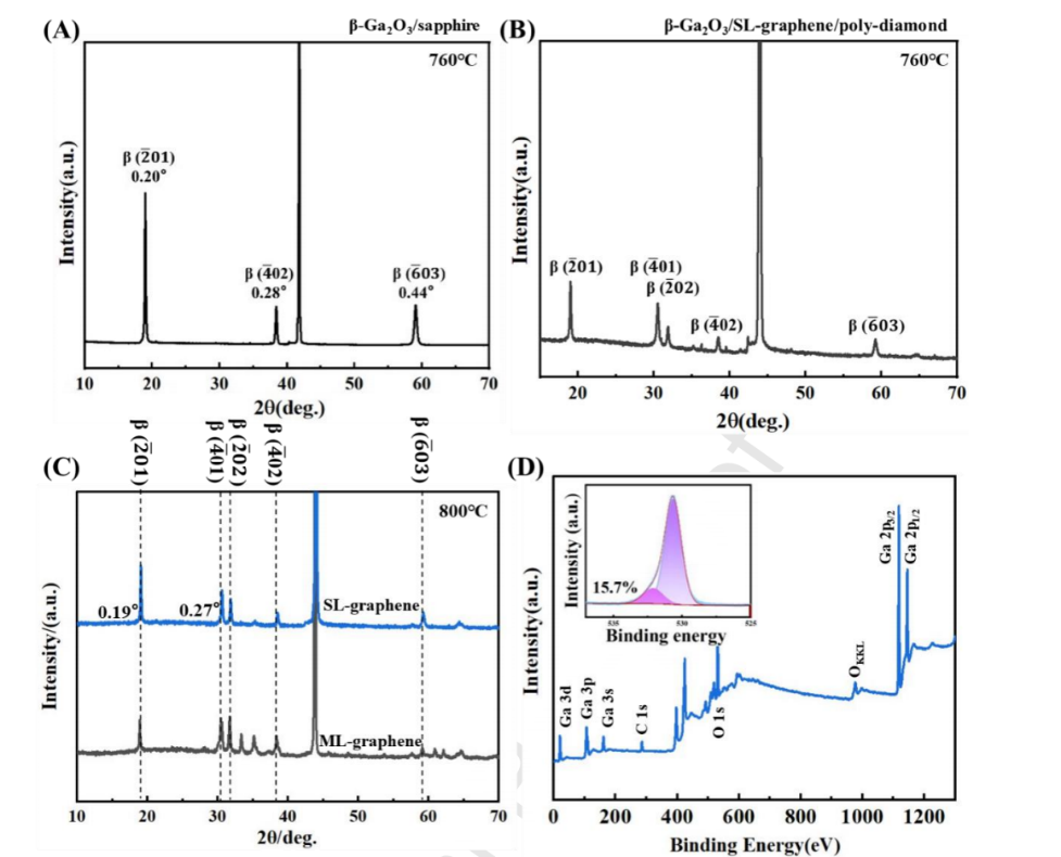
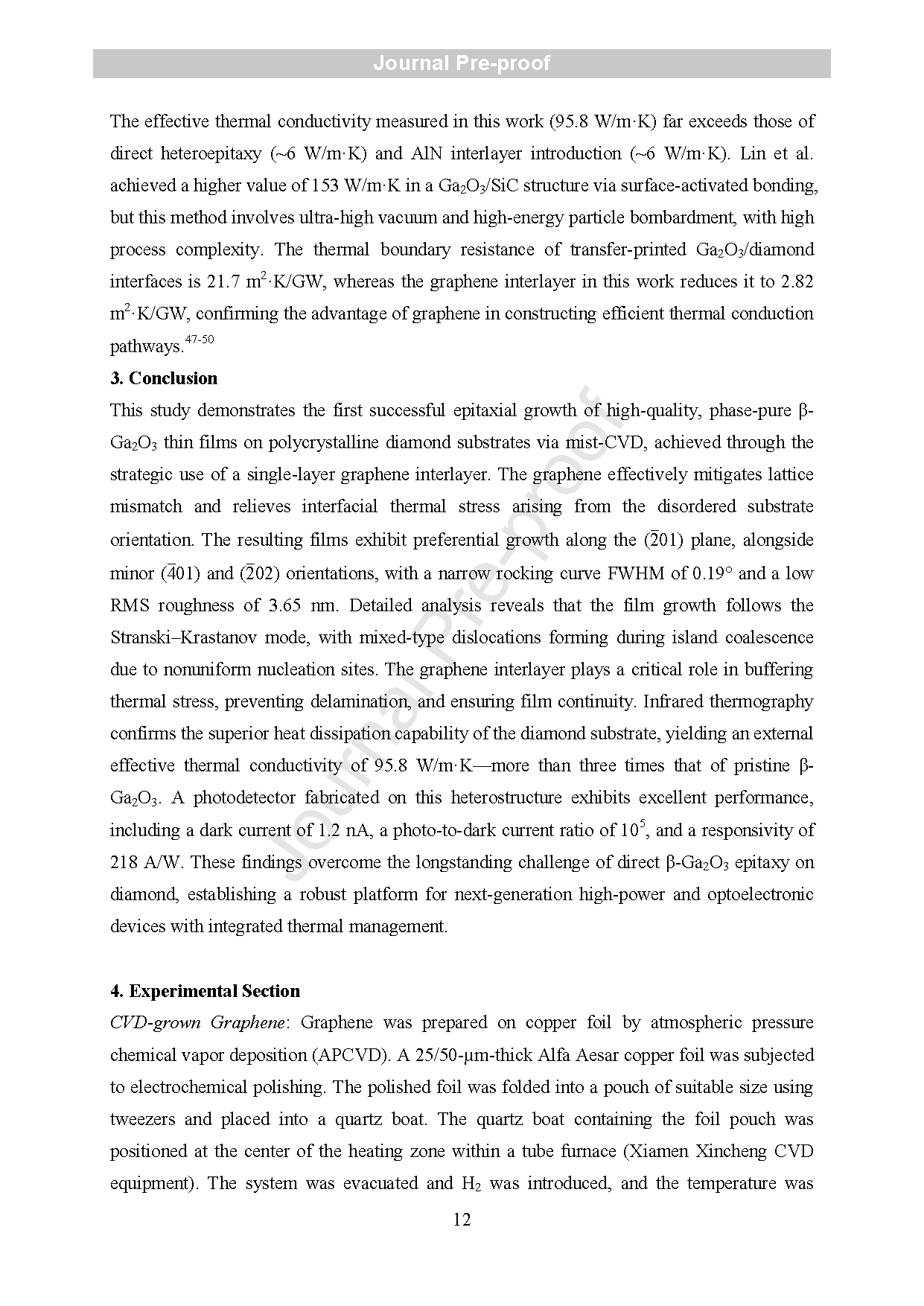
Figure 1. (A) X-ray diffraction (XRD) spectra of single-crystal β-Ga₂O₃ thin films epitaxially grown on c-sapphire. (B) XRD spectra of β-Ga₂O₃ thin films grown on SL-graphene/polydiamond at 760°C using vdW epitaxy. (C) XRD spectra of β-Ga₂O₃ thin films grown on graphene with various numbers of layers using vdW epitaxy. (D) X-ray photoelectron spectroscopy (XPS) results obtained at an O₂ flow rate of 600 sccm, along with O1s XPS spectra (inset).
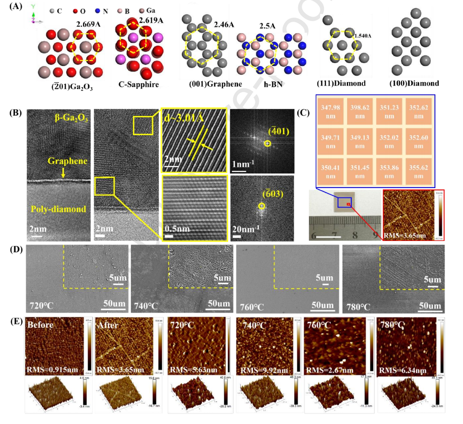
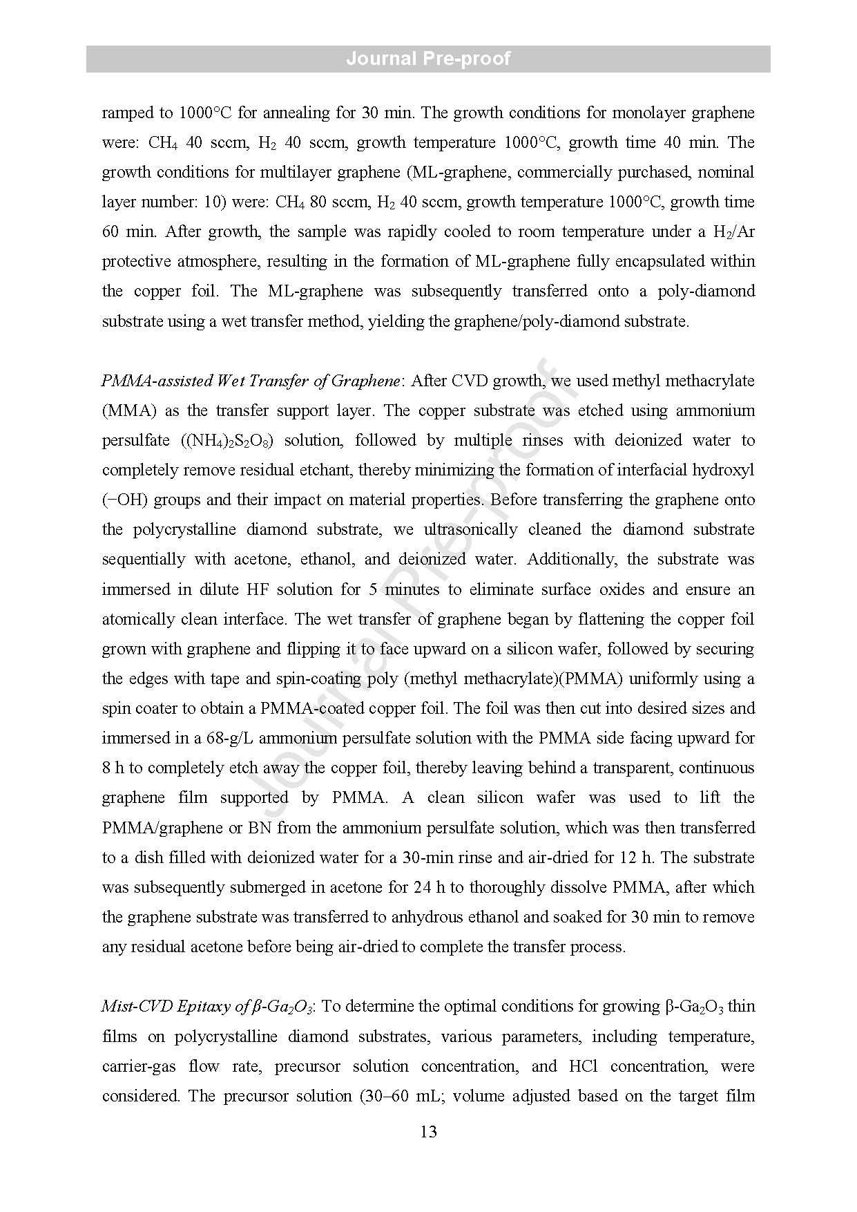
Figure 2. (A) Atomic schematics (top views) of (2̅01) β-Ga₂O₃ and various substrates with 2D materials. (B) High-magnification TEM images of coalescence boundaries in β-Ga₂O₃ thin films with different crystal orientations grown using vdW epitaxy. (C) Epitaxial β-Ga₂O₃ film on graphene/polycrystalline diamond: photograph, AFM topography, and thickness mapping. (D) SEM morphology of β-Ga₂O₃/graphene/poly-diamond substrates at deposition temperatures of 720°C-780°C. (E) AFM surface topography of the SL-graphene/polydiamond substrate before and after epitaxial growth of β-Ga₂O₃.
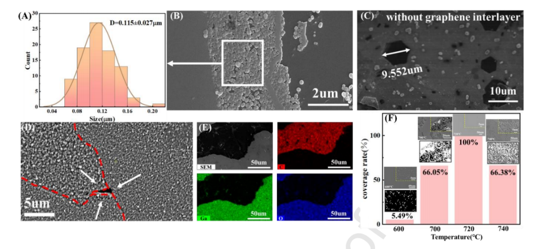
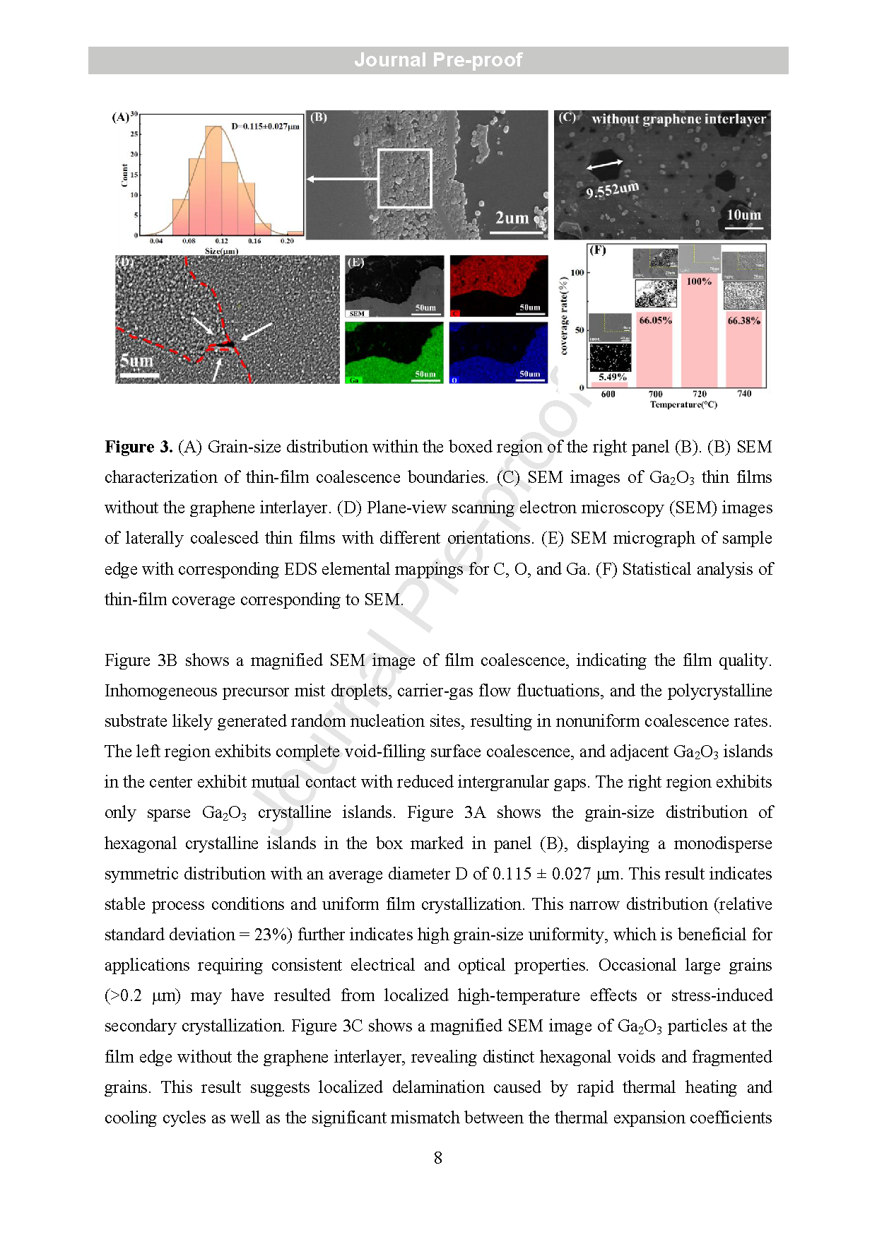
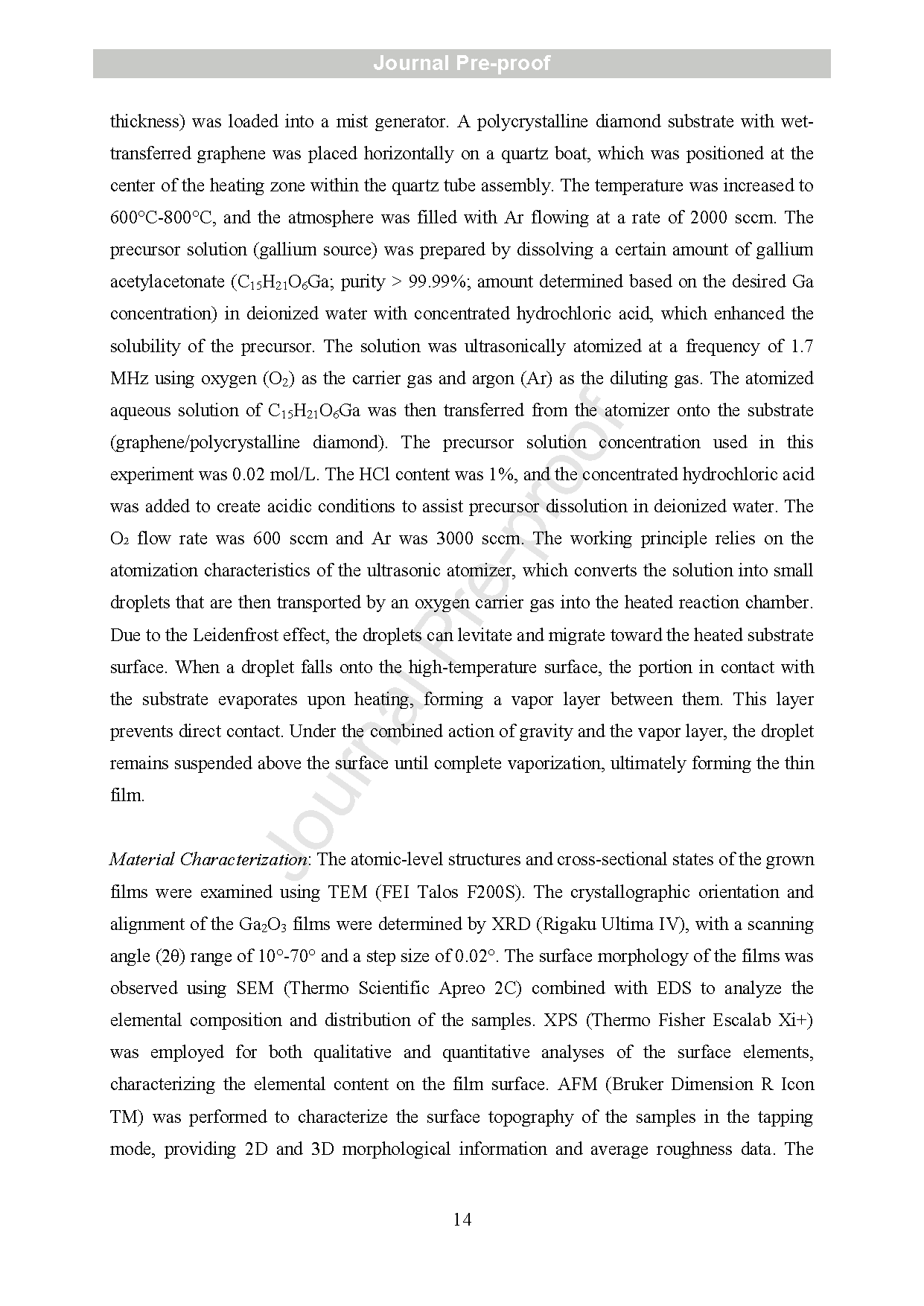
Figure 3. (A) Grain-size distribution within the boxed region of the right panel (B). (B) SEM characterization of thin-film coalescence boundaries. (C) SEM images of Ga₂O₃ thin films without the graphene interlayer. (D) Plane-view scanning electron microscopy (SEM) images of laterally coalesced thin films with different orientations. (E) SEM micrograph of sample edge with corresponding EDS elemental mappings for C, O, and Ga. (F) Statistical analysis of thin-film coverage corresponding to SEM.
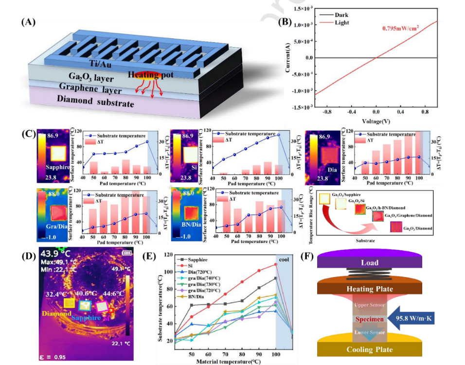
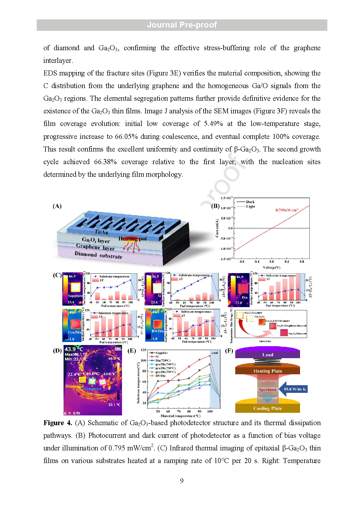
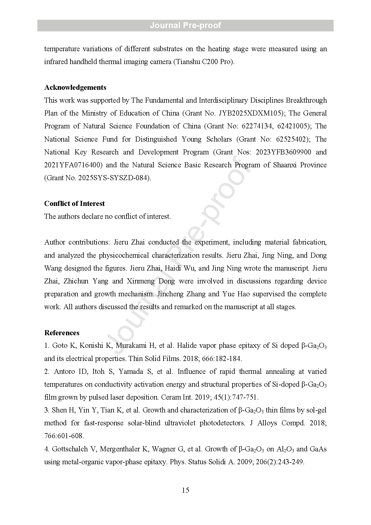
Figure 4. (A) Schematic of Ga₂O₃-based photodetector structure and its thermal dissipation pathways. (B) Photocurrent and dark current of photodetector as a function of bias voltage under illumination of 0.795 mW/cm². (C) Infrared thermal imaging of epitaxial β-Ga₂O₃ thin films on various substrates heated at a ramping rate of 10°C per 20 s. Right: Temperature difference (ΔT=TS-TP) between film surface (TS) and heating stage (TP), and variation of thin film surface temperature with heating stage temperature. Finally, a comparison of the temperature rise on heating stage for epitaxial β-Ga₂O₃ grown on different substrates is presented. (D) Infrared thermal imaging of epitaxial β-Ga₂O₃ thin films on various substrates (E) Temperature variation curves measured every 20 s relative to substrate temperature. (F) Schematic of measuring external equivalent thermal conductivity via the heat flow meter method.
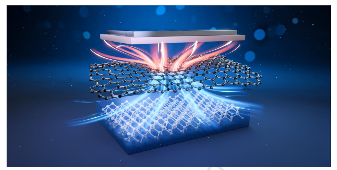
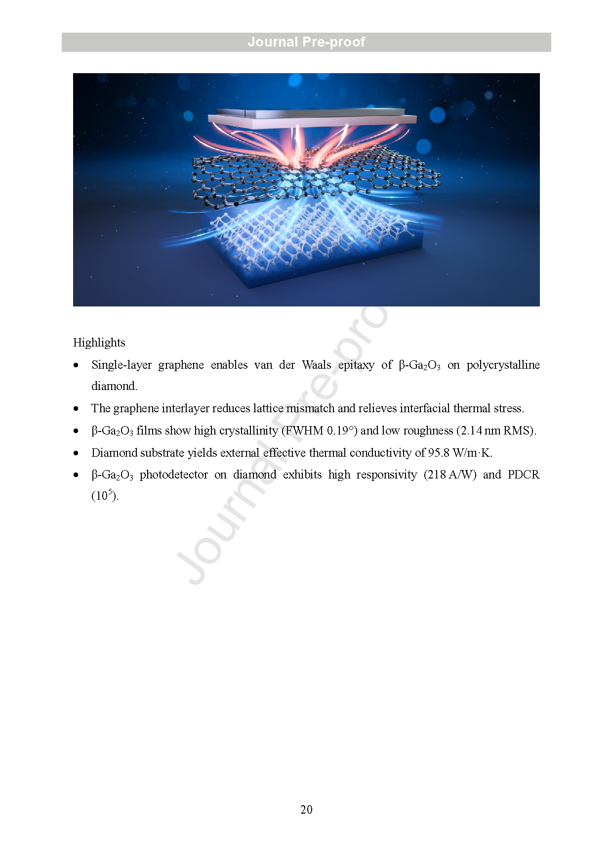
Figure 5.Schematic diagram of van der Waals epitaxial β-Ga₂O₃/graphene/polycrystalline diamond heterostructure and heat transfer path
DOI :
doi.org/10.1016/j.diamond.2026.114026
Instruction
Official Account

Cooperation
Top
