


From August 26 to 28, 2026, PCIM Asia Shenzhen 2026 was held at the Shenzhen World Exhibition & Convention Center. At the “Frontier Technologies of Ultra-Wide-Bandgap Semiconductors Forum,” jointly organized by PCIM Asia and the Shenzhen Pinghu Laboratory, Qi Hongji, a researcher at the Shanghai Institute of Optics and Fine Mechanics, Chinese Academy of Sciences, and Founder and Chairman of Fujia Gallium, was invited to deliver a keynote presentation entitled “Industrialization Progress of Large-Size, High-Quality Gallium Oxide Single-Crystal Substrates and Epitaxial Wafers.”
During the presentation, Qi Hongji provided a systematic overview of the latest industrialization progress of gallium oxide substrates and epitaxial wafers in China and abroad, emphasizing that high-quality seed crystals are critical for controlling crystal orientation and improving crystal quality.
The first- through third-generation semiconductor materials that have achieved large-scale commercial application today employ different crystal-growth methods, but all rely on seed crystals to grow high-quality single crystals. This approach avoids the inherent limitations of spontaneous nucleation, where the number of nuclei is difficult to control, potentially resulting in polycrystalline growth, twinning, and random crystal orientations.
The seed-guided Vertical Bridgman (VB) method enables the growth of low-cost, large-size, and high-quality gallium oxide crystals, making it better suited to future large-scale mass production.
Seed-Guided Growth: Ensuring Crystal Quality
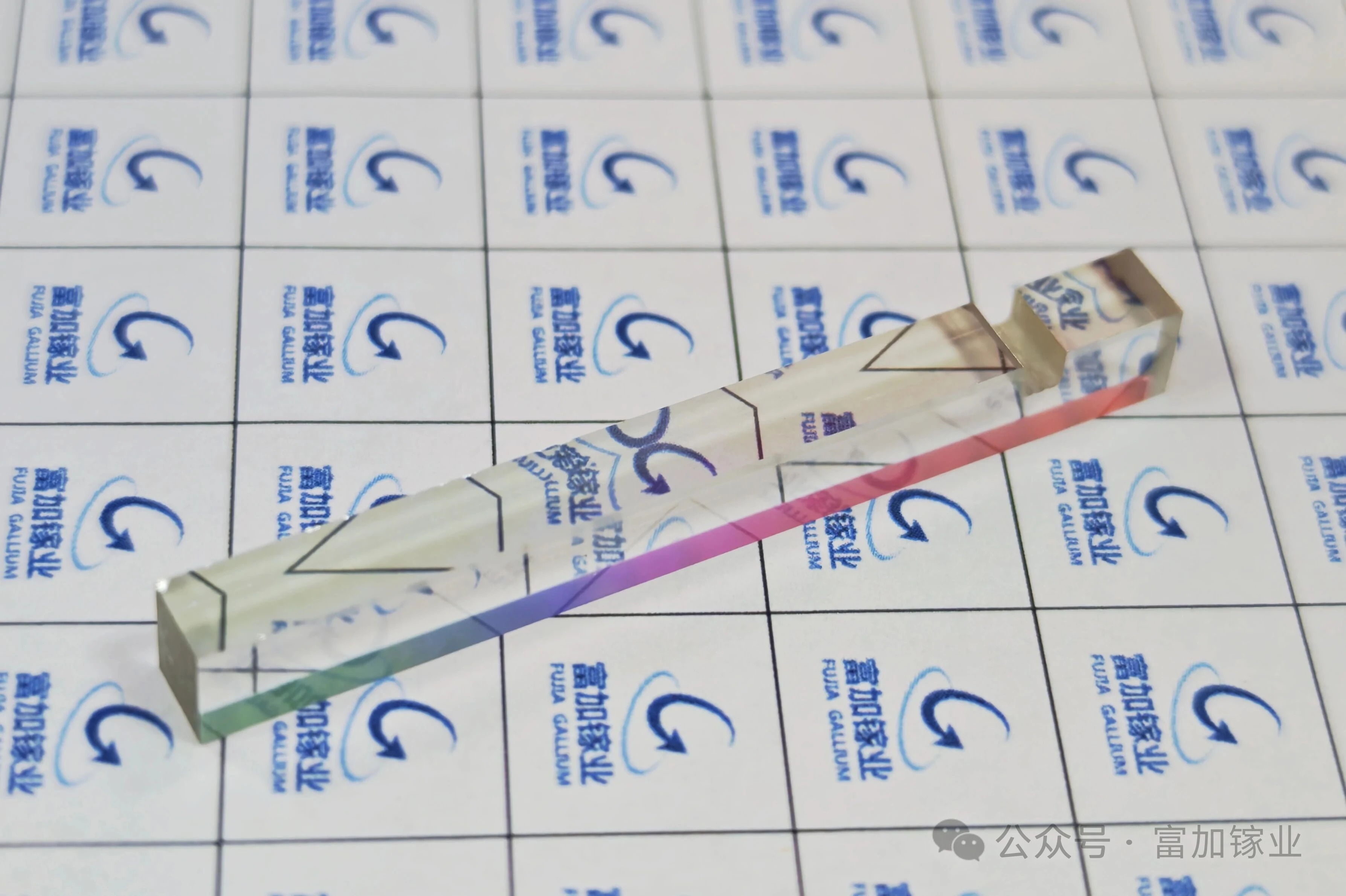
Seed crystals play a central role as a “genetic template” in crystal growth. By providing a well-defined lattice framework, the seed guides atoms in the melt to deposit in an ordered manner, thereby determining the final crystallographic orientation of the crystal. Physically, this eliminates the random orientations associated with spontaneous nucleation without a seed, thereby preventing problems such as twinning and grain boundaries. In addition, when combined with processes such as necking or shouldering, seed-guided growth can take advantage of dislocation climb to exclude defects originating from the seed from the newly grown crystal, enabling a process of “self-purification” and achieving an extremely low dislocation density. More importantly, the use of a seed crystal eliminates the dependence of crystal growth on random nucleation events, ensuring a high degree of consistency from batch to batch. For first- through third-generation semiconductor single-crystal materials that have achieved large-scale production—including single-crystal silicon, gallium arsenide, indium phosphide, silicon carbide, and gallium nitride—seed-guided growth methods are universally employed in their mature manufacturing processes.
β-Ga₂O₃ exhibits pronounced crystal anisotropy. In addition to the advantages described above, seed-guided growth enables the target crystallographic orientation to be preset at the beginning of growth by selecting a seed crystal with a specific orientation. It has been clearly demonstrated that seed-assisted Vertical Bridgman (VB) growth can produce β-Ga₂O₃ single crystals with various orientations, including (100), (010), (001), and (011). Japan-based Novel Crystal Technology (NCT) has also identified the flexibility to produce substrates with different crystallographic orientations as one of the key advantages of the VB method.
“Iridium-Free Growth”: A Key Consideration for Commercialization Costs
Edge-defined film-fed growth (EFG) is one of the earliest and most well-developed crystal-growth methods in the gallium oxide field, offering advantages including high crystal quality and extensive experimental validation. Although iridium consumption during the crystal-growth process is relatively limited, the large upfront investment required for iridium crucibles when expanding production capacity has become one of the major obstacles to the future large-scale adoption of the EFG method.
The VB method does not require iridium crucibles. On the one hand, this significantly reduces capital investment. On the other hand, the VB method offers a stable thermal field and a relatively small temperature gradient during crystal growth, while also enabling repeated reuse of thermal-field consumables, substantially reducing material preparation costs.
Recently, Fujia Gallium successfully grew a 6-inch gallium oxide single crystal with a uniform diameter and a thickness exceeding 70 mm, which can significantly increase substrate output per growth run and further reduce the cost of individual single-crystal substrates. Fujia Gallium has also achieved 12-inch single-crystal growth, further contributing to the reduction in single-crystal substrate prices.
Qi Hongji stated that the price of 6-inch gallium oxide single-crystal substrates is expected to be brought below RMB 800 in the future.
Research Progress on VB-Grown Gallium Oxide Overseas
Outside China, companies and research institutions including Novel Crystal Technology (NCT) in Japan, Shinshu University, and the U.S. Air Force Research Laboratory (AFRL) have conducted extensive research on gallium oxide crystal growth using the VB method and on the properties of the resulting crystals. Their findings have confirmed that the VB method can produce high-quality crystals with excellent substrate performance.
Shinshu University conducted a systematic comparative study of gallium oxide crystals grown by the VB and EFG methods, finding that the full width at half maximum (FWHM) of VB-grown crystals was lower than that of EFG-grown crystals. After chemically etching the crystals, the researchers found that the defects observed in VB-grown crystals were similar to those in EFG-grown crystals, but the defects in the VB-grown crystals were smaller in size.
The U.S. Air Force Research Laboratory (AFRL) further carried out end-to-end validation from substrates and epitaxy to devices using VB-grown gallium oxide crystals. The resulting devices demonstrated high yield and good consistency in electrical performance, providing evidence that VB-grown gallium oxide crystals are reliable and capable of supporting the large-scale development of gallium oxide power electronic devices.
Progress and Validation of Fujia Gallium’s VB Method
Fujia Gallium was among the earliest companies in China to pursue the VB method for gallium oxide crystal growth. Within just a few years, the company has successively achieved technological breakthroughs in single-crystal growth from 3-inch to 12-inch wafers.
The latest 6-inch single-crystal substrates produced by Fujia Gallium were tested by a third-party organization. The substrates exhibited an XRD full width at half maximum (FWHM) of 38.71 arcsec, an average resistivity of 16.4 mΩ·cm, and an in-plane resistivity non-uniformity of 6.8%, meeting the substrate requirements of the silicon carbide industry.
In addition, Fujia Gallium was the first company in China to establish a team dedicated to the industrialization of MOCVD technology, with its epitaxial film performance reaching an internationally leading level. Comparative validation of homoepitaxial growth by MOCVD showed that epitaxial layers grown on gallium oxide substrates prepared by the VB and EFG methods exhibited comparable performance in key metrics, including crystal quality, surface morphology, and electrical transport properties. These results demonstrate that VB-grown gallium oxide substrates can meet the substrate-quality requirements for high-quality homoepitaxial growth.
Furthermore, vertical power Schottky barrier diodes (SBDs) fabricated using the resulting epitaxial wafers achieved a power figure of merit (PFOM) of 3.07 GW/cm², the highest value reported to date among publicly available international studies of MOCVD-grown gallium oxide epitaxial-wafer-based SBDs. The company’s independently developed homoepitaxial wafers also supported the Jiufengshan Laboratory of Materials Science in developing a lateral gallium oxide MOSFET with a breakdown voltage exceeding 9,000 V, setting a new world record.
Looking ahead, Fujia Gallium plans to further integrate artificial intelligence (AI) methods into the VB growth process. The company has already filed eight VB-process-related patent applications, including four international patent applications, as well as four equipment-related patent applications. By incorporating AI into crystal-growth equipment, the equipment is expected to acquire self-learning capabilities, enabling continuous improvement in crystal and epitaxial-layer quality.
About Fujia Gallium
Hangzhou Fujia Gallium Technology Co., Ltd. was established on December 31, 2019. The company takes “Bringing Better Materials to the World” as its vision, and commits to the industrialization of ultra-wide bandgap semiconductor gallium oxide materials.
The company is a national high-tech enterprise, a Zhejiang Provincial specialized, refined, unique and innovative small and medium-sized enterprise, and a "quasi-unicorn" enterprise. It has undertaken many national and provincial-level projects from the Ministry of Science and Technology, National Development and Reform Commission, Ministry of Industry and Information Technology and other departments. It has obtained 67 authorized patents at home and abroad. It is the initiator and the first drafting unit of national standards in China’s gallium oxide industry. A series of important achievements achieved by the company in promoting gallium oxide industrialization have been reported and publicized by well-known media such as CCTV, People’s Daily, Xinhuanet, Science and Technology Daily, China Securities Journal and The Paper.
Instruction
Official Account

Cooperation
Top
