


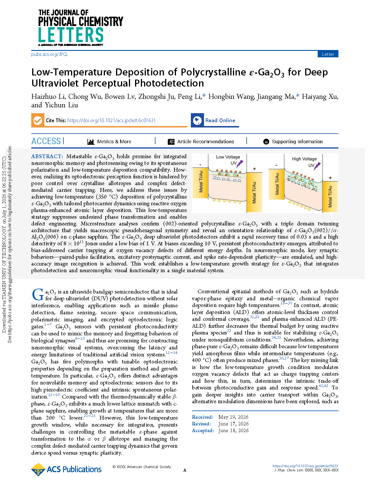
Researchers from Northeast Normal University have published a dissertation titled "Low-Temperature Deposition of Polycrystalline ε-Ga₂O₃ for Deep Ultraviolet Perceptual Photodetection" in The Journal of Physical Chemistry Letters.
Background
ε-Ga₂O₃ is a metastable gallium oxide polymorph with intrinsic spontaneous polarization, which can realize both deep ultraviolet photodetection and neuromorphic memory, and has wide applications in secure UV communication and neuromorphic computing. Traditional β-Ga₂O₃ growth requires high temperature, which cannot be integrated with low-temperature flexible or silicon-based chips. Although ε-Ga₂O₃ has smaller lattice mismatch with sapphire, mixed α/β phases easily form during deposition. Disordered oxygen vacancy defects lead to uncontrollable carrier trapping, making it hard to balance fast photoresponse and synaptic plasticity. Previous studies only realize single-function devices, and low-temperature monolithic integration of dual-mode ε-Ga₂O₃ optoelectronic devices is rarely reported, forming an important research gap.
Abstract
Metastable ε-Ga₂O₃ holds promise for integrated neuromorphic memory and photosensing owing to its spontaneous polarization and low-temperature deposition compatibility. However, realizing its optoelectronic perception function is hindered by poor control over crystalline allotropes and complex defect-mediated carrier trapping. Here, we address these issues by achieving low-temperature (350 °C) deposition of polycrystalline ε-Ga₂O₃ with tailored photocarrier dynamics using reactive oxygen plasma-enhanced atomic layer deposition. This low-temperature strategy suppresses undesired phase transformation and enables defect engineering. Microstructure analyses confirm (002)-oriented polycrystalline ε-Ga₂O₃ with a triple domain twinning architecture that yields macroscopic pseudohexagonal symmetry and reveal an orientation relationship of ε-Ga₂O₃(002)//α-Al₂O₃ (006) on c-plane sapphire. The ε-Ga₂O₃ deep ultraviolet photodetectors exhibit a rapid recovery time of 0.03 s and a high detectivity of 8 × 10¹¹ Jones under a low bias of 1 V. At biases exceeding 10 V, persistent photoconductivity emerges, attributed to bias-addressed carrier trapping at oxygen vacancy defects of different energy depths. In neuromorphic mode, key synaptic behaviors paired-pulse facilitation, excitatory postsynaptic current, and spike rate-dependent plasticity are emulated, and high-accuracy image recognition is achieved. This work establishes a low-temperature growth strategy for ε-Ga₂O₃ that integrates photodetection and neuromorphic visual functionality in a single material system.
Highlights
Low-temperature (350 °C) PE-ALD growth of phase-pure (002)-oriented polycrystalline ε-Ga₂O₃on c-plane sapphire is realized.
Triple-domain twinning microstructure of ε-Ga₂O₃and its epitaxial matching relationship with sapphire are systematically characterized.
Bias-switchable dual-mode device functions including fast DUV detection and neuromorphic synaptic simulation are demonstrated.
The fabricated device achieves 83.5% CIFAR-10 image recognition accuracy in simulated convolutional neural network.
Conclusion
In summary, we demonstrate the low-temperature growth of ε-Ga₂O₃ films at 350 °C via PE-ALD. Cross-sectional TEM and FFT analyses confirm the formation of polycrystalline (002)-oriented ε-Ga₂O₃ with a triple-domain twinning architecture that yields macroscopically pseudohexagonal symmetry and reveal a well-defined orientation relationship of ε-Ga₂O₃(002)//α-Al₂O₃(006) with the c-plane sapphire substrate. The ε-Ga₂O₃ photodetectors exhibit bias-switchable dual-mode functionality. At a low bias of 1 V, the device delivers a fast photoresponse (0.03 s) and high detectivity (8 × 10¹¹ Jones). At an increased bias of 30 V, the enhanced electric field selectively addresses oxygen vacancy defects at different energy depths, amplifying persistent photoconductivity and transitioning the device into a neuromorphic computing mode, where synaptic behaviors (PPF, EPSC, and SRDP) and multistate conductance modulation are emulated. A simulated CNN based on device characteristics achieves 83.5% accuracy on CIFAR-10. These results establish that PE-ALD-grown ε-Ga₂O₃ is a promising candidate for integrated photoelectric sensing and neuromorphic computing platforms.
Project Support
This work was supported by the National Key Research and Development Program (2021YFA0716404), the National Natural Science Foundation of China (12474164, 52302166, and 62404038), the 111 Project (B25030), and the Research Projects of the Education Office of Jilin Province (JJKH20261332KJ) and Changchun City (25GNYZ60).
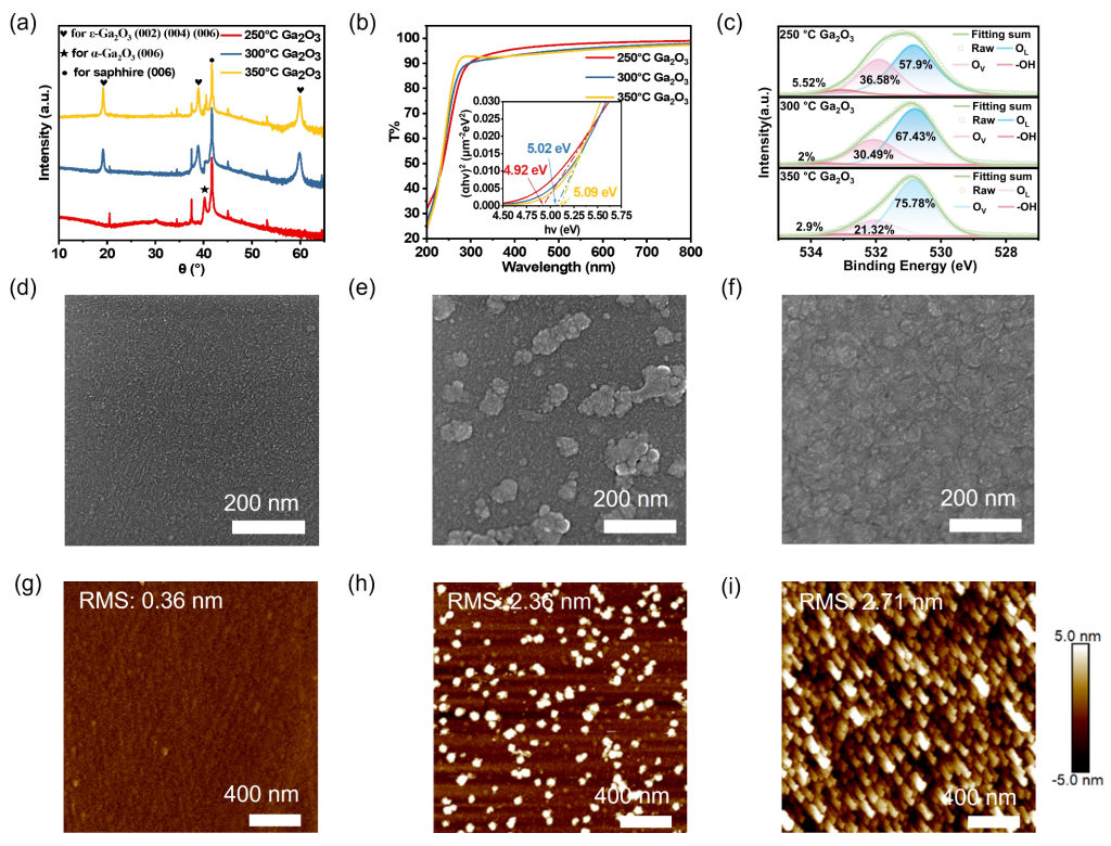
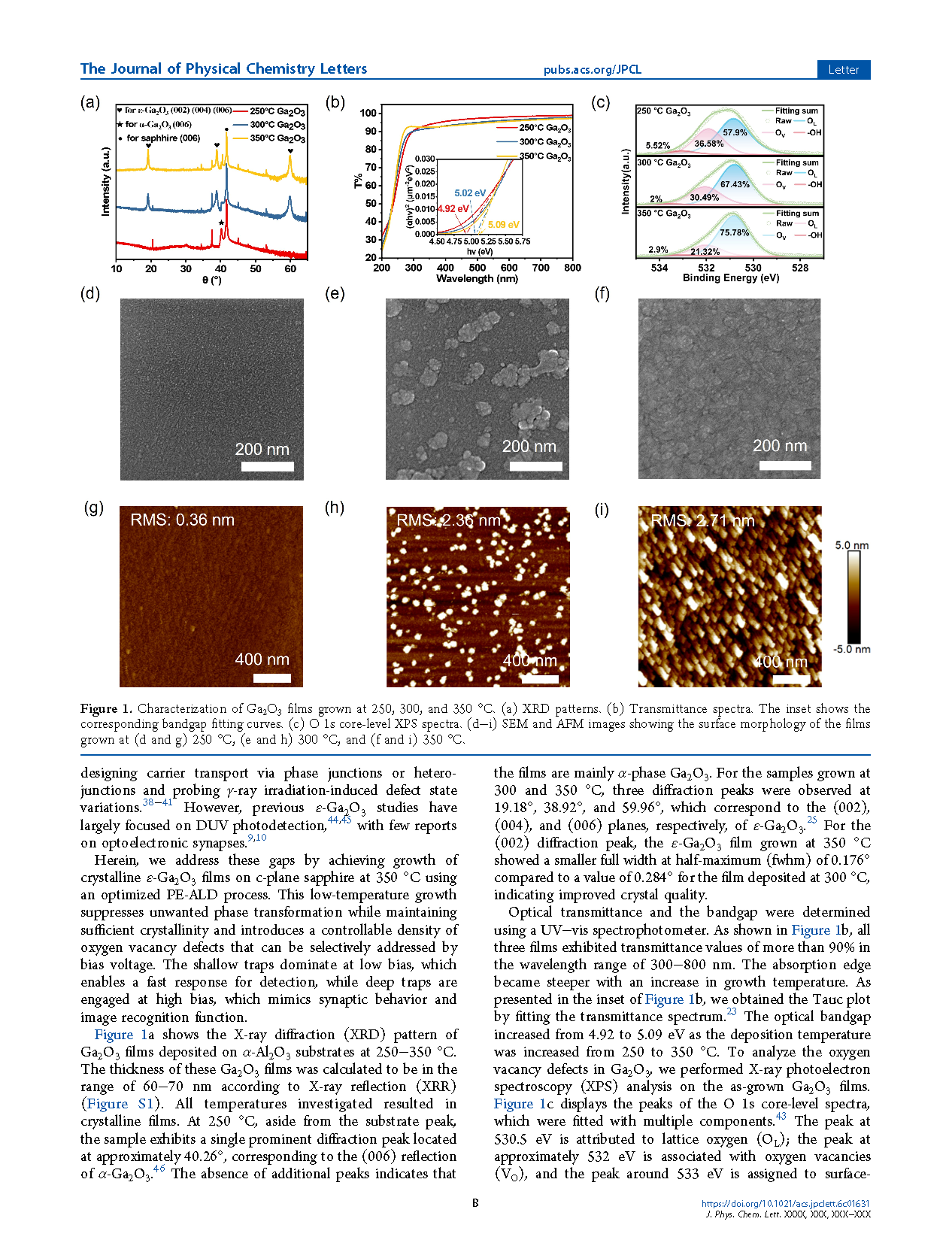
Figure 1. Characterization of Ga₂O₃ films grown at 250, 300, and 350 °C. (a) XRD patterns. (b) Transmittance spectra. The inset shows the corresponding bandgap fitting curves. (c) O 1s core-level XPS spectra. (d−i) SEM and AFM images showing the surface morphology of the films grown at (d and g) 250 °C, (e and h) 300 °C, and (f and i) 350 °C.
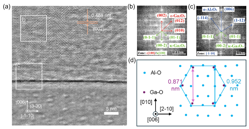
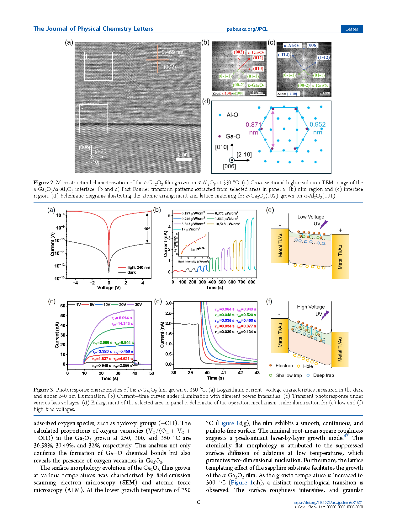
Figure 2. Microstructural characterization of the ε-Ga₂O₃ film grown on α-Al₂O₃ at 350 °C. (a) Cross-sectional high-resolution TEM image of the ε-Ga₂O₃/α-Al₂O₃ interface. (b and c) Fast Fourier transform patterns extracted from selected areas in panel a: (b) film region and (c) interface region. (d) Schematic diagrams illustrating the atomic arrangement and lattice matching for ε-Ga₂O₃(002) grown on α-Al₂O₃(001).
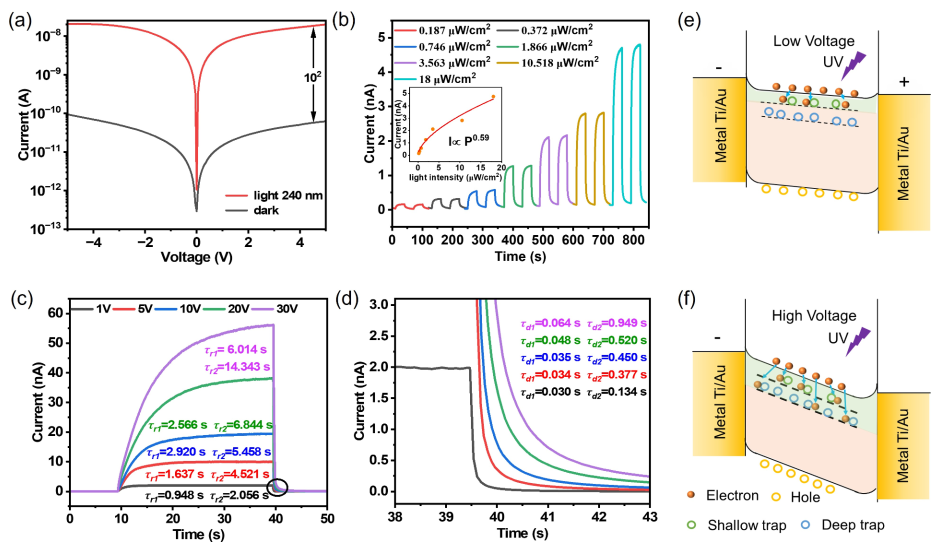
Figure 3. Photoresponse characteristics of the ε-Ga₂O₃ film grown at 350 °C. (a) Logarithmic current-voltage characteristics measured in the dark and under 240 nm illumination. (b) Current−time curves under illumination with different power intensities. (c) Transient photoresponse under various bias voltages. (d) Enlargement of the selected area in panel c. Schematic of the operation mechanism under illumination for (e) low and (f) high bias voltages.
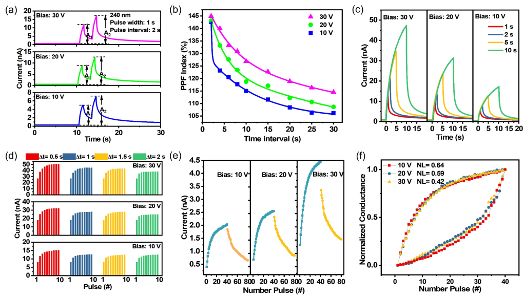
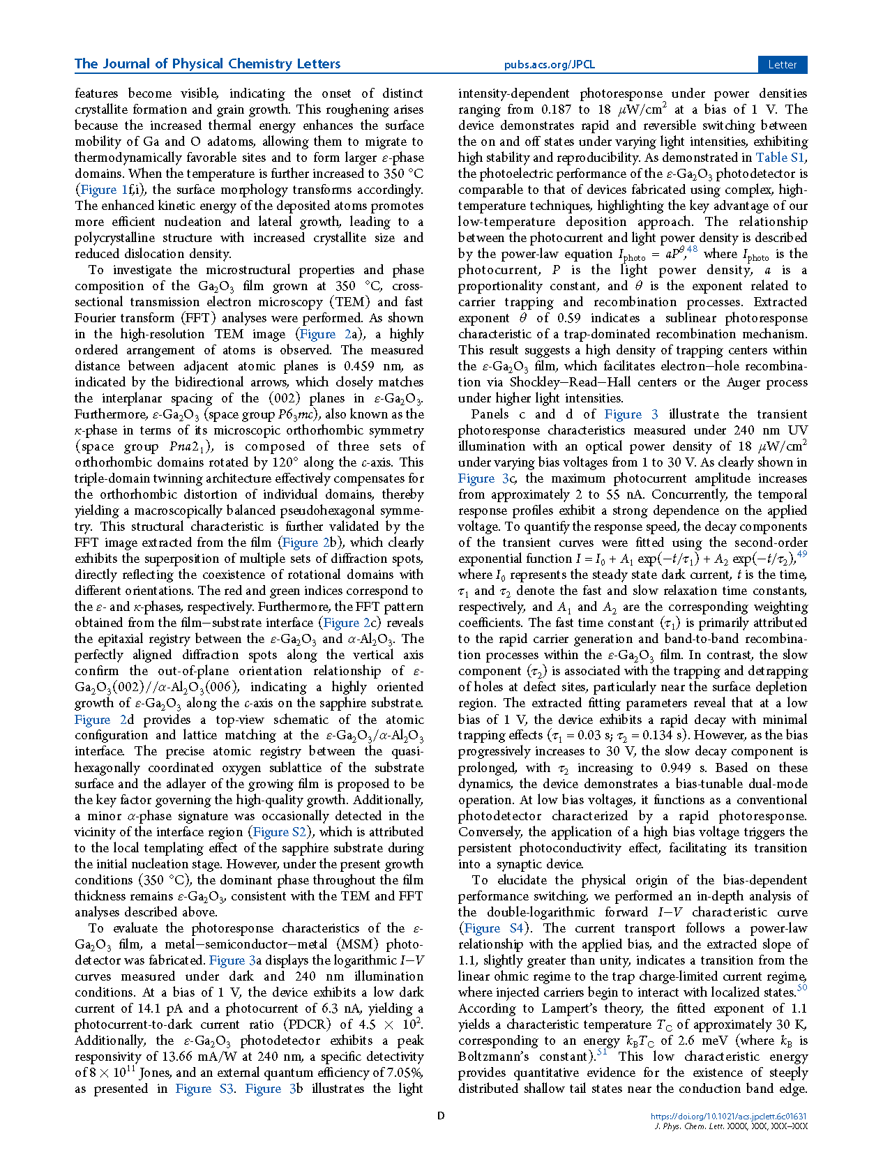
Figure 4. Emulation of biological synaptic functions using the ε-Ga₂O₃ photodetector under DUV pulsed illumination. (a) Change in current triggered by paired light pulses. (b) PPF index vs pulse interval. (c) EPSC under UV pulsed illumination at various times and bias voltages. (d) Current response induced by light pulses with intervals ranging from 0.5 to 2 s under different bias voltages. (e) Optical potentiation and electrical depression behaviors (optical power density of 18 μW/cm² and depression voltage of −1 V). (f) Normalized optical potentiation/electrical depression comparison at various bias voltages.
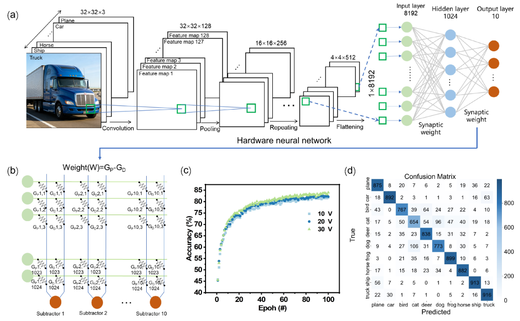
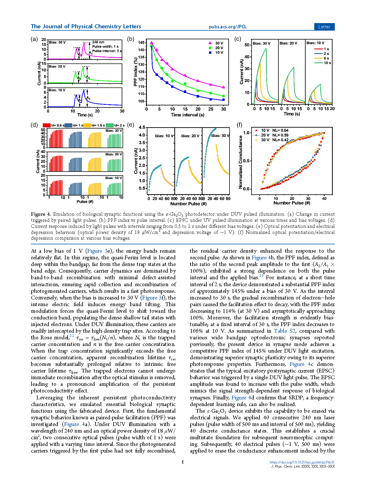
Figure 5. CIFAR-10 data set recognition task. (a) CIFAR-10 data set and convolutional neural network comprising convolutional, pooling, and fully connected layers. (b) Hardware neural network comprising the optoelectronic synapse devices for the fully connected CNN layer. (c) Recognition accuracy for the CIFAR-10 data set. (d) Confusion matrix obtained at a bias of 30 V.
DOI:
doi.org/10.1021/acs.jpclett.6c01631
Instruction
Official Account

Cooperation
Top
