


Researchers from Northeast Normal University, Agency for Science Technology and Research, The City College of New York have published a paper titled "Enhanced Performance of β-Ga₂O₃/GaN Heterojunction UV Photodetector via Introducing an Amorphous GaON Nucleation Layer in the Reverse Substitution Growth" in Advanced Optical Materials.
Background
Solar-blind ultraviolet light with wavelengths ranging from 200–280 nm cannot reach the Earth’s surface and features strong anti-interference capability, which is widely applied in fire early warning, missile guidance and ozone monitoring. As an ultra-wide bandgap semiconductor, β-Ga₂O₃ possesses a bandgap matching the solar-blind region and breakdown electric field up to 8 MV/cm, making it a core candidate for solar-blind photodetectors. The β-Ga₂O₃/GaN heterojunction forms built-in electric field to separate photogenerated carriers efficiently, delivering superior performance to pure Ga₂O₃ devices. Conventional direct high-temperature reverse substitution oxidation for GaN substrates brings ultra-fast oxidation rates, inducing massive oxygen vacancy defects, uneven film thickness and high surface roughness. These defects accelerate carrier recombination and degrade responsivity and detectivity severely. Existing modification strategies cannot simultaneously improve crystal quality and suppress interfacial defects. This work adopts low-temperature pre-annealing to form an amorphous GaON nucleation layer on GaN surface in-situ, regulating oxygen diffusion and homogenizing substitution reactions to reduce oxygen vacancy density. High-quality, low-defect β-Ga₂O₃ thin films are fabricated, and two types of photodetectors (MSM lateral structure and vertical heterojunction) are manufactured with comprehensively optimized optoelectronic performance.
Abstract
A high detectivity (~10¹⁶ Jones) and enhanced spectral selectivity UV photodetector of β-Ga₂O₃/GaN heterojunction is achieved by introducing an ultra-thin GaON amorphous nucleation layer during the initial stage of the reverse substitution growth of β-Ga₂O₃. The amorphous GaON layer is formed by oxidizing the GaN surface at a low temperature of 900◦C under oxygen atmosphere, which as a nucleation layer promote its oriented transformation from GaN into β-Ga₂O₃ with smoother, denser surfaces at high oxidizing temperature. The β-Ga₂O₃ with (-201) preferred orientation, obtained by the introduction of the amorphous nucleation layer, displays narrower linewidths and lower root mean square of the surface roughness (7.51 nm →4.62 nm). The concentration of oxygen vacancies in β-Ga₂O₃ has been found to be significantly reduced, and the surface morphology considerably improved. Subsequently, the fabrication of metal-semiconductor-metal (MSM) and vertical-structure β-Ga₂O₃/GaN heterojunction ultraviolet photodetectors was carried out. The MSM-type device displayed a responsivity of 174 A/W and a detectivity of 1.56×10¹⁶ Jones at 20 V bias, with transient response times of 0.35 ms (rise time) and 65.7 ms (decay time). The heterojunction device showed a responsivity of 14.5 A/W and a detectivity of 10¹⁴ Jones, with transient response reaching the millisecond level.
Highlights
A 900 ℃ low-temperature pre-annealing strategy is proposed to grow amorphous GaON nucleation layer on GaN surface in-situ, homogenize high-temperature substitution oxidation and drastically cut oxygen vacancy density in β-Ga₂O₃ films;
The surface RMS roughness reduces from 7.51 nm to 4.62 nm after modification, the (-201) preferred orientation crystal quality is greatly improved, and interfacial lattice mismatch stress is effectively relieved;
The MSM lateral photodetector achieves responsivity of 174 A/W and detectivity of 1.56×10¹⁶ Jones under 20 V bias, with state-of-the-art weak-light detection performance among similar thin-film devices;
Vertical β-Ga₂O₃/GaN heterojunction photodetectors with obvious rectification are fabricated simultaneously, realizing millisecond-scale fast photoresponse for high-voltage UV detection applications;
The devices exhibit outstanding long-term air storage stability, dense low-defect film prevents interface contact degradation, offering a universal modification route for high-performance Ga₂O₃ optoelectronics via thermal oxidation.
Conclusion
A pre-annealing treatment was introduced before high temperature thermal oxidation in this work, resulting in the formation of an amorphous GaON layer. This layer subsequently transformed β-Ga₂O₃ with a preferred orientation of (-201). With a cyclic oxidation method of two consecutive high temperature annealing to prepare β-Ga₂O₃ films, resulting in lower surface roughness, fewer defects, and higher crystal quality. The performances of MSM-type and vertical structure n-β-Ga₂O₃/n-GaN heterojunction photodetectors were sufficiently improved with high responsivity (R=174 A/W) ultra-high specific detectivity (D* ~ 10¹⁶ Jones) and a fast response speed of milliseconds. These results confirm that the cyclic oxidation method effectively improves the flatness and reduces defects. Consequently, the method provides a possibility for obtaining high-quality, wide-bandgap oxide semiconductors and high-performance photodetectors based on thermal oxidation.
Project Support
This work was supported by the National Natural Science Foundation of China (no. 62274027, 62404039, 52272157), the 111 Center (B25030), the funding from Jilin Province (no. 20220502002 GH), and the Open Research Fund of Song Shan Lake (2023SLABFK03). J.T. acknowledges the funding support from the National Research Foundation, Singapore, under NRF-CRP26-2021-0004.
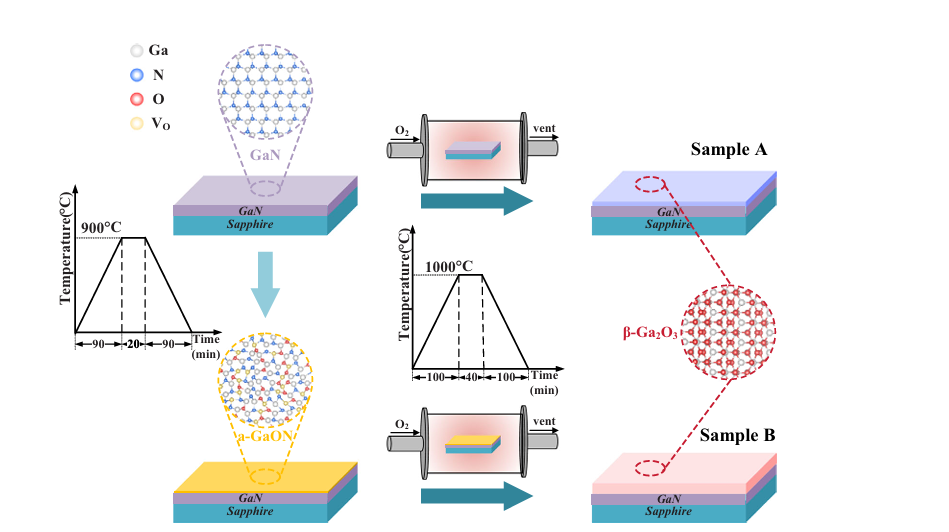
Figure 1 Schematic diagrams of the preparation of Sample A and Sample B. Left part shows amorphous GaON layer formed on GaN surface via pre-annealing at 900 ℃, right part displays cross-sectional layered structure of two thin films after high-temperature oxidation
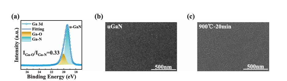
Figure 2 (a) Ga 3d XPS spectra of untreated u-GaN; (b) SEM surface morphology of u-GaN without annealing; (c) SEM surface morphology of u-GaN after annealing at 900 ℃ for 20 min
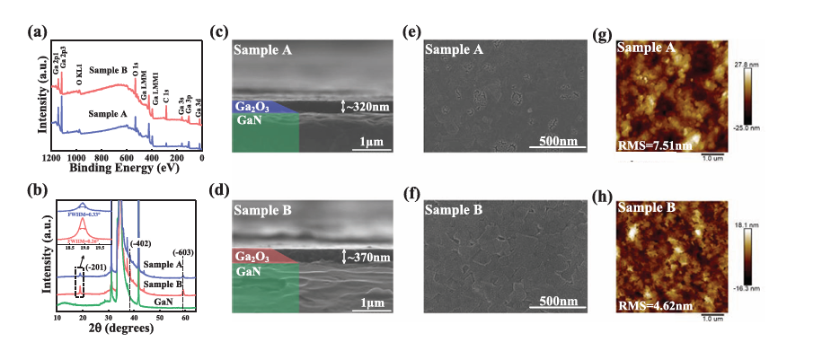
Figure 3 (a) XPS spectra of Sample A and Sample B; (b) XRD spectra of u-GaN, Sample A and Sample B, the inset shows enlarged view of (-201) diffraction peak; For Sample A and Sample B: (c, d) Cross-sectional SEM images; (e, f) Surface SEM images; (g, h) AFM surface morphology with scanning area of 5×5 µm², RMS roughness values are marked
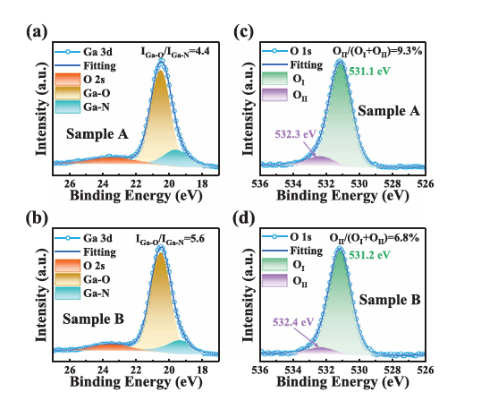
Figure 4 Core-level XPS spectra for Sample A and Sample B after etching: (a, b) Ga 3d spectra; (c, d) O 1s spectra with oxygen vacancy proportion labeled
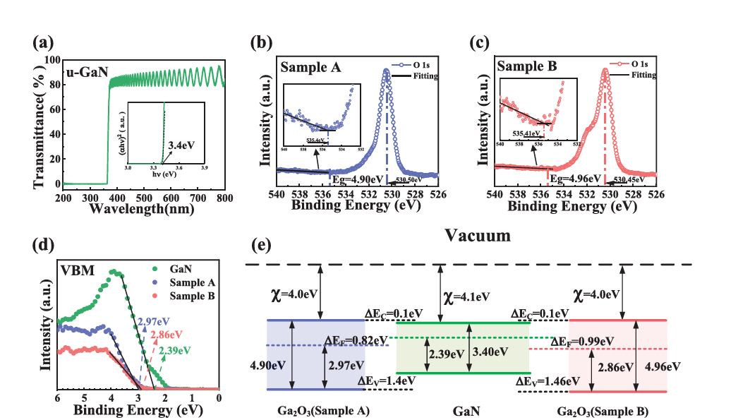
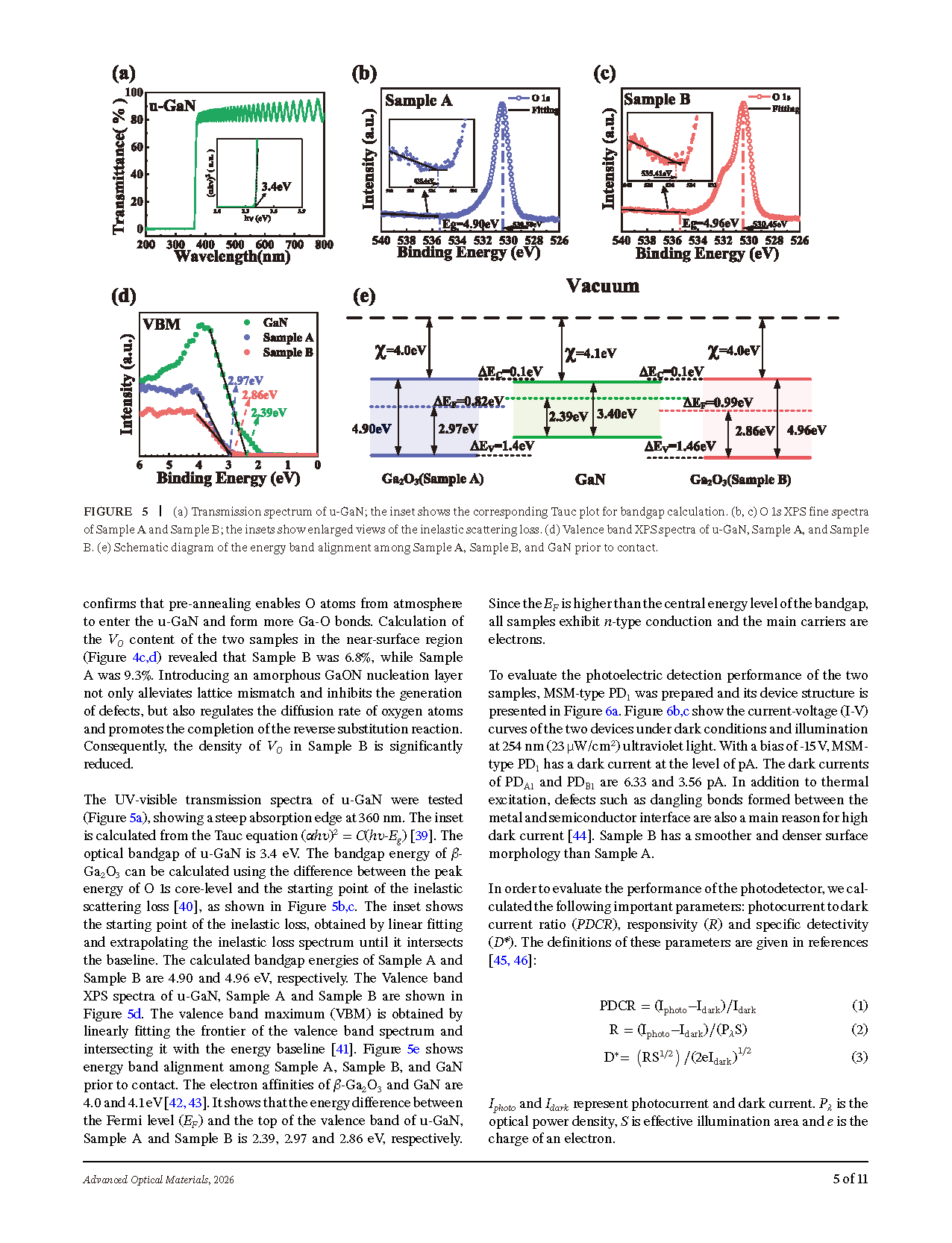
Figure 5 (a) Transmission spectrum of u-GaN, the inset shows Tauc plot for bandgap calculation; (b, c) O 1s fine spectra of Sample A and Sample B, insets present fitting curves of inelastic loss onset; (d) Valence band XPS spectra of u-GaN, Sample A and Sample B; (e) Schematic diagram of energy band alignment among GaN, Sample A and Sample B before contact
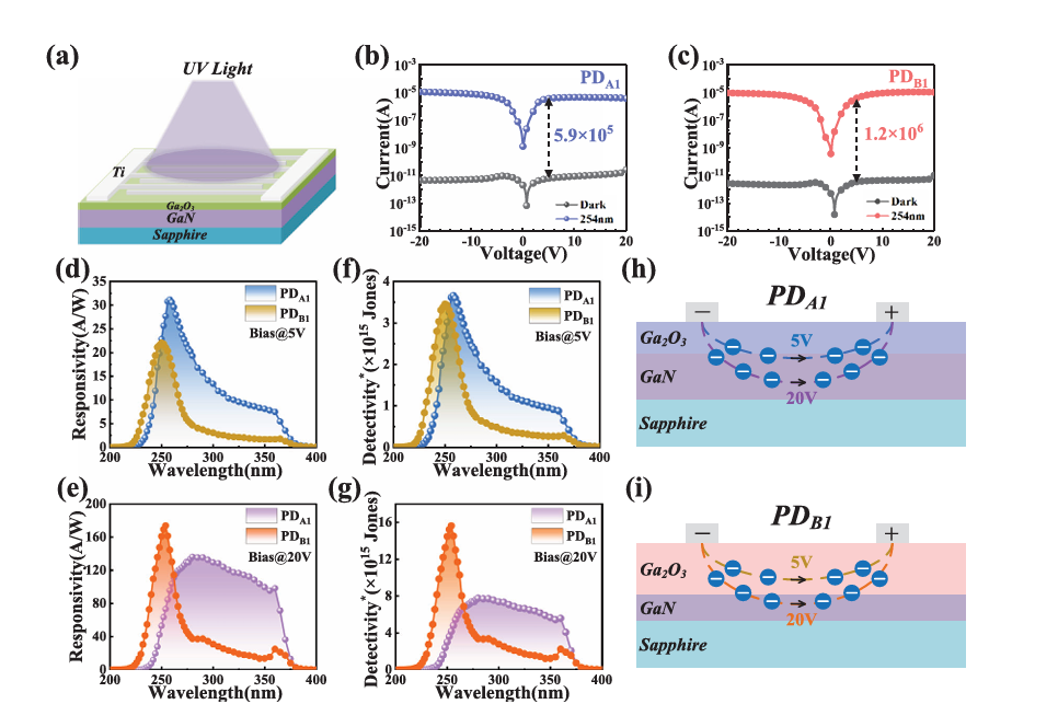
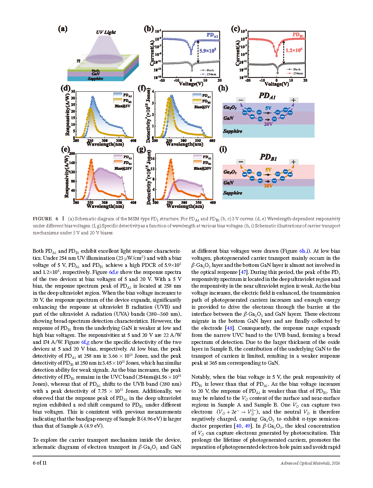
Figure 6 (a) Schematic diagram of MSM-type PD₁ structure; For PDA1 and PDB1: (b, c) I-V curves under dark and 254 nm UV illumination; (d, e) Wavelength-dependent responsivity under different bias voltages; (f, g) Specific detectivity as a function of wavelength at various bias voltages; (h, i) Schematic illustrations of carrier transport mechanisms under 5 V and 20 V biases
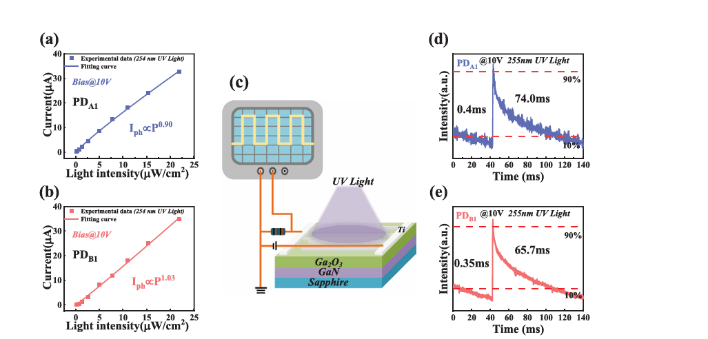
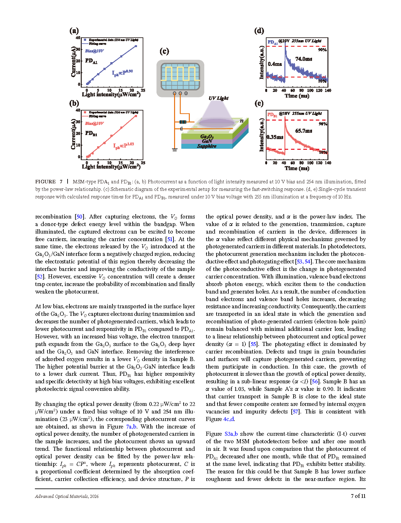
Figure 7 (a, b) Photocurrent versus light intensity curves of two MSM devices at 10 V bias under 254 nm UV light with power-law fitting; (c) Schematic diagram of experimental setup for transient response measurement; (d, e) Single-cycle transient photoresponse at 10 V bias with rise and decay time marked
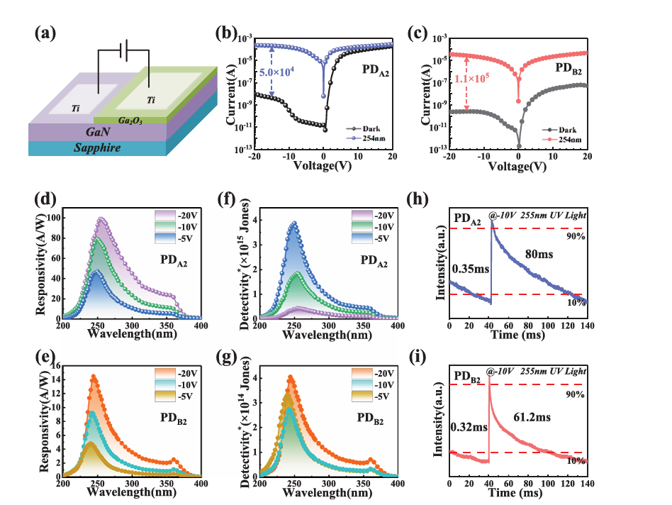
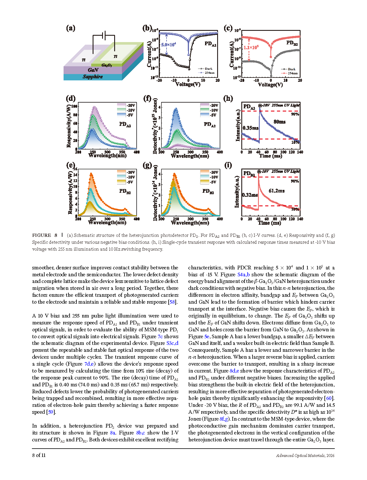
Figure 8 (a) Schematic structure of heterojunction PD₂ device; For PDA2 and PDB2: (b, c) I-V curves under dark and 254 nm UV light; (d, e) Responsivity under various negative bias voltages; (f, g) Specific detectivity under various negative bias voltages; (h, i) Single-cycle transient response at -10 V with time parameters labeled
DOI:
doi.org/10.1002/adom.71497
Instruction
Official Account

Cooperation
Top
