


Semiconductor Materials Testing
A Critical Enabler for R&D and Mass Production
During semiconductor manufacturing, even subtle variations in material properties, microscopic defects, trace impurities, or abnormal crystal-domain states can lead to critical issues such as leakage current, breakdown, and device lifetime degradation, ultimately affecting the stability of end products and the pace of industrialization.
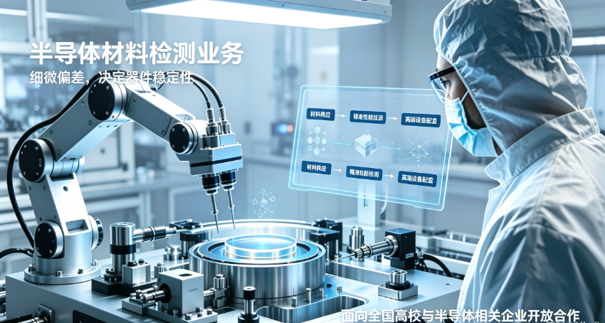
To address key pain points in semiconductor materials testing, Wonder-Sino has launched its semiconductor materials testing services, establishing a closed-loop service chain spanning “Material Supply → Precision Performance Testing → Advanced Equipment Support.” The service is now open to universities, research institutions, and semiconductor-related enterprises nationwide for collaboration.
Corporate Strength
15 Years of Industry Expertise and Experience
Guided by the philosophy of “Leading with Technology, Connecting Gallium to the World,” Wonder-Sino Group has remained committed to providing customers across the wide-bandgap semiconductor industry with cutting-edge materials, equipment, and process technologies.
As one of the earliest companies in China to establish a presence in the fourth-generation semiconductor sector, particularly in gallium oxide (Ga₂O₃) materials and equipment, Wonder-Sino has continuously integrated technologies and resources across the industry to deliver comprehensive “Materials + Equipment + Processes” solutions for its customers.
By combining technology introduction with independent R&D, Wonder-Sino works closely with leading domestic universities and research institutions to leverage their R&D capabilities, while collaborating with industry-leading companies to tackle key technical challenges. By precisely connecting critical nodes in the industrialization process, Wonder-Sino is building a Ga₂O₃ industrial ecosystem and driving the transition of gallium oxide materials from the laboratory to large-scale applications.
Testing Services
Five Core Advantages to Address Key Testing Challenges
1.Authoritative Accreditations
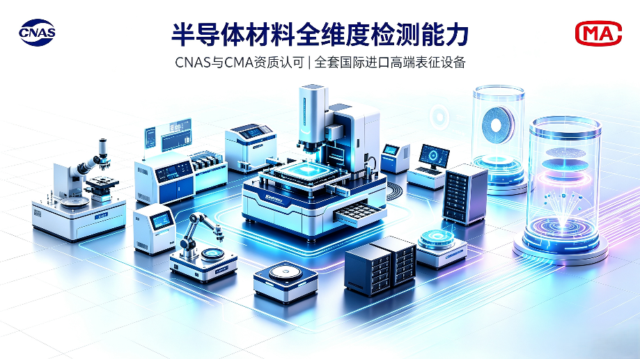
Our laboratory holds both CNAS and CMA accreditation and has established a standardized testing system in accordance with ISO/IEC 17025. For semiconductor materials covered by the accredited scope, we can issue authoritative test reports carrying both CNAS and CMA accreditation.
CMA accreditationcarries statutory validity in China and can be used for product quality assessment, technical achievement evaluation, and forensic or judicial appraisal.
CNAS accreditationis part of the ILAC Mutual Recognition Arrangement (MRA). CNAS-accredited reports are recognized by more than 100 international accreditation bodies through equivalent recognition mechanisms, supporting product exports, overseas industry–academia–research collaboration, and data requirements for international journal publications.
2.Advanced Testing Equipment
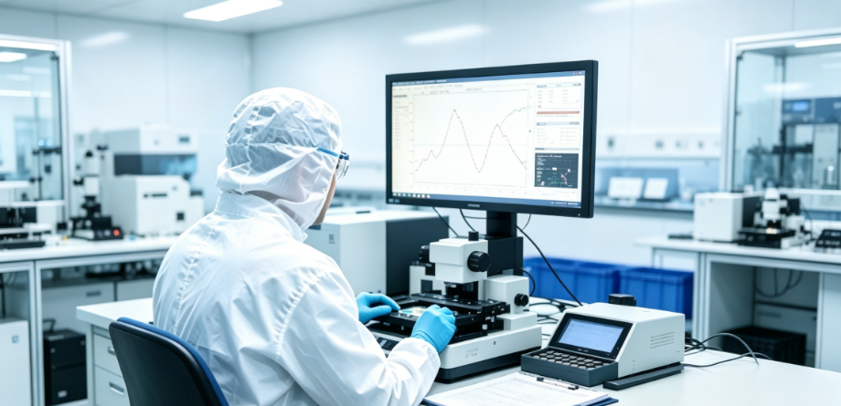
Equipped with a comprehensive range of mainstream internationally sourced testing instruments, our laboratory ensures high testing accuracy and covers a full spectrum of characterization capabilities, including electrical and optical properties, crystal structure, surface defects, and trace elemental impurities. Our hardware capabilities are benchmarked against those of leading research institutes and laboratories supporting high-volume semiconductor production lines.
3.Comprehensive Semiconductor Material Coverage
We provide a comprehensive range of semiconductor materials testing services, supporting samples including substrates, epitaxial layers, thin films, optical crystals, and heterostructures. Our capabilities cover multidimensional characterization of surface quality and morphology, electrical and optical properties, trace impurities, crystal structure, and defects.
4.Reliable Data & Professional Expertise
A fully standardized testing and quality-control process ensures rigorous management across sample handling, testing, and data processing. With more than 10 years of experience in semiconductor characterization, our engineers are well versed in testing and analysis methodologies for different types of semiconductor materials and can develop targeted testing and experimental protocols based on specific sample characteristics and application requirements.
5. Efficient & Hassle-Free Service
We provide one-stop, end-to-end testing services with flexible turnaround times and expedited options available when needed. Dedicated service personnel track each project and provide timely progress updates throughout the process. All samples and data are handled under strict confidentiality, with samples returned upon request or disposed of in compliance with applicable requirements after testing.
Business Consultation

Ms. Tang | +86 156 2060 2509
Email: tn@wonder-sino.com
Group Website: www.wonder-sino.com
Core Services:
Ga₂O₃ Substrates | Ga₂O₃ Epitaxy | Crystal Growth Equipment | Processing Equipment | CNAS/CMA-Accredited Semiconductor Materials Testing Services
Instruction
Official Account

Cooperation
Top
