


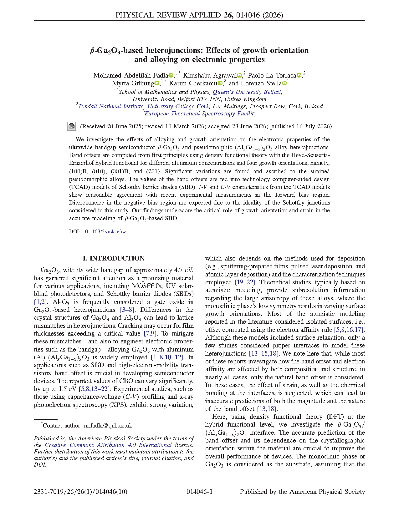
Researchers from the Queen's University Belfast、Tyndall National Institute, University College Cork and European Theoretical Spectroscopy Facility have published a dissertation titled "β-Ga₂O₃-based heterojunctions: Effects of growth orientation and alloying on electronic properties" in Physical Review Applied.
Background
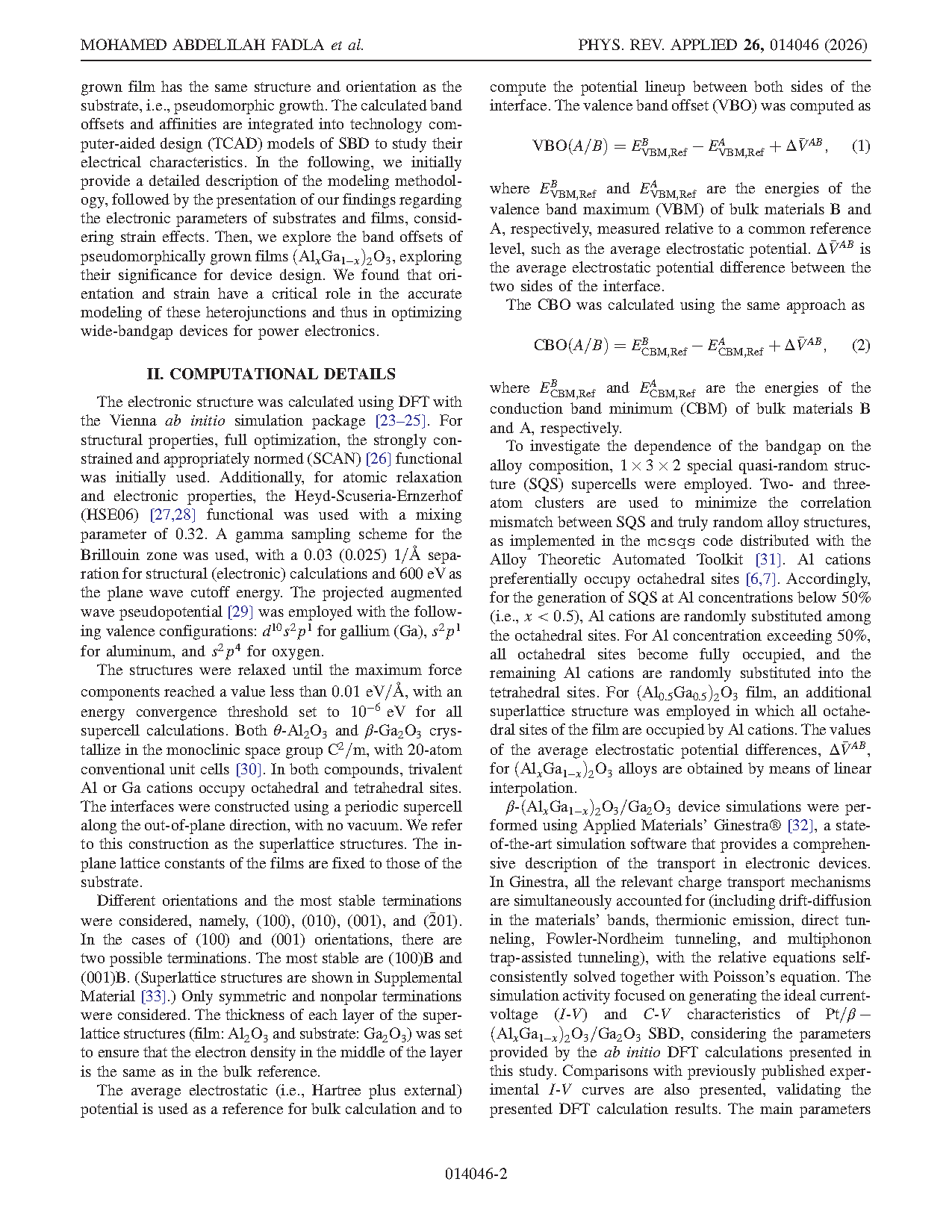
Ga₂O₃, with its wide bandgap of approximately 4.7 eV, has garnered significant attention as a promising material for various applications, including MOSFETs, UV solar-blind photodetectors, and Schottky barrier diodes (SBDs). Al₂O₃ is frequently considered a gate oxide in Ga₂O₃-based heterojunctions. Differences in the crystal structures of Ga₂O₃ and Al₂O₃ can lead to lattice mismatches in heterojunctions. Cracking may occur for film thicknesses exceeding a critical value. To mitigate these mismatches—and also to engineer electronic properties such as the bandgap—alloying Ga₂O₃ with aluminum (Al) (AlₓGa₁₋ₓ)₂O₃ is widely employed.
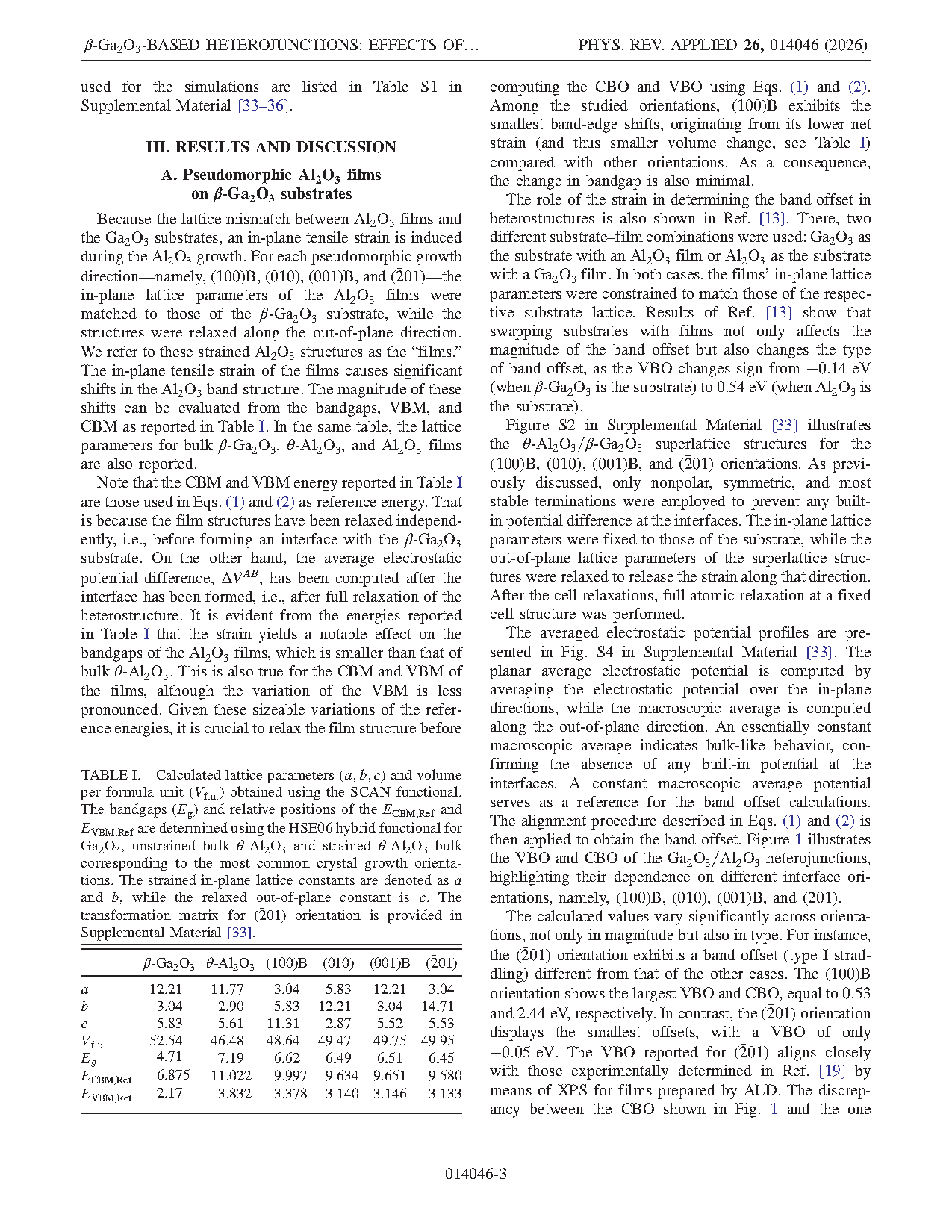
In applications such as SBD and high-electron-mobility transistors, band offset is crucial in developing semiconductor devices. The reported values of CBO can vary significantly, by up to 1.5 eV. Experimental studies, such as those using capacitance-voltage (C-V) profiling and x-ray photoelectron spectroscopy (XPS), exhibit strong variation, which also depends on the methods used for deposition and the characterization techniques employed. Theoretical studies, typically based on atomistic modeling, provide subresolution information regarding the large anisotropy of these alloys. Most of the atomistic modeling reported in the literature considered isolated surfaces, i.e., offset computed using the electron affinity rule. Although these models included surface relaxation, only a few studies considered proper interfaces to model these heterojunctions. In nearly all cases, only the natural band offset is considered, where the effect of strain, as well as the chemical bonding at the interfaces, is neglected, which can lead to inaccurate predictions of both the magnitude and the nature of the band offset.
Here, using density functional theory (DFT) at the hybrid functional level, the team investigates the β-Ga₂O₃/(AlₓGa₁₋ₓ)₂O₃ interface. The accurate prediction of the band offset and its dependence on the crystallographic orientation within the material are crucial to improve the overall performance of devices.
Abstract
We investigate the effects of alloying and growth orientation on the electronic properties of the ultrawide bandgap semiconductor β-Ga₂O₃ and pseudomorphic (AlₓGa₁₋ₓ)₂O₃ alloy heterojunctions. Band offsets are computed from first principles using density functional theory with the Heyd-Scuseria-Ernzerhof hybrid functional for different aluminum concentrations and four growth orientations, namely, (100)B, (010), (001)B, and (-201). Significant variations are found and ascribed to the strained pseudomorphic alloys. The values of the band offsets are fed into technology computer-aided design (TCAD) models of Schottky barrier diodes (SBD). I-V and C-V characteristics from the TCAD models show reasonable agreement with recent experimental measurements in the forward bias region. Discrepancies in the negative bias region are expected due to the ideality of the Schottky junctions considered in this study. Our findings underscore the critical role of growth orientation and strain in the accurate modeling of β-Ga₂O₃-based SBD.
Highlights
①Superlattice structures are adopted to directly model real heterojunction interfaces rather than isolated slabs, and pseudomorphic strain effects are self-consistently incorporated into band offset calculations, overcoming the long-standing neglect of strain and interfacial chemical bonding.
②Significant variations in band offsets across four growth orientations ((100)B, (010), (001)B, and (-201)) are systematically revealed, with the (-201) orientation exhibiting a unique type-I straddling band offset—a result that explains the up-to-1.5 eV discrepancy in reported CBO values in the literature.
③DFT-derived band offset parameters are directly fed into TCAD device simulations, bridging the atomic scale and the device scale. The I-V and C-V characteristics of SBDs under different orientations are simulated and validated against experimental measurements.
④Orientation-dependent tailoring of device performance is demonstrated—the (100) orientation yields an ultrahigh ION/IOFF ratio, whereas the (-201) orientation achieves a low turn-on voltage and high forward current, offering theoretical guidance for orientation engineering of power devices.
⑤Al substitution is shown to primarily modulate the conduction band (O 2p states exert little influence on the valence band), and the transition of transport mechanisms from diffusion to tunneling across different bias regions is elucidated.
Conclusion
We have conducted computational modeling using the Heyd-Scuseria-Ernzerhof hybrid functional and technology computer-aided design models to investigate band offset, I-V, and C-V for different growth orientations and alloy compositions in Ga₂O₃/(AlₓGa₁₋ₓ)₂O₃ heterojunctions. Strain from lattice mismatch affects both VBM and CBM, with distinct behaviors observed across (-201), (010), (001), and (100) orientations due to the high anisotropy of the monoclinic phase. We examined the effect of the strain on band offset by incorporating its effect on bulk energy levels and the potential lineup at the interface to ensure a consistent reference. The high sensitivity to growth orientation and strain may justify the discrepancies in previously published results. Additionally, we report C-V and I-V simulations for Ga₂O₃/(Al₀.₂₅Ga₀.₇₅)₂O₃/Pt SBD across the four growth orientations, revealing significant orientation dependence given the different materials' electron affinities and the resulting conduction band offsets. To validate our findings, we simulated and compared with experimental I-V results for Al concentrations of 22% and 21%, achieving reasonable agreement in the forward bias. These results provide insights into the device structure and the potential defect and highlight the critical role of orientation and strain engineering in optimizing wide-bandgap devices for power electronics.
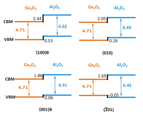
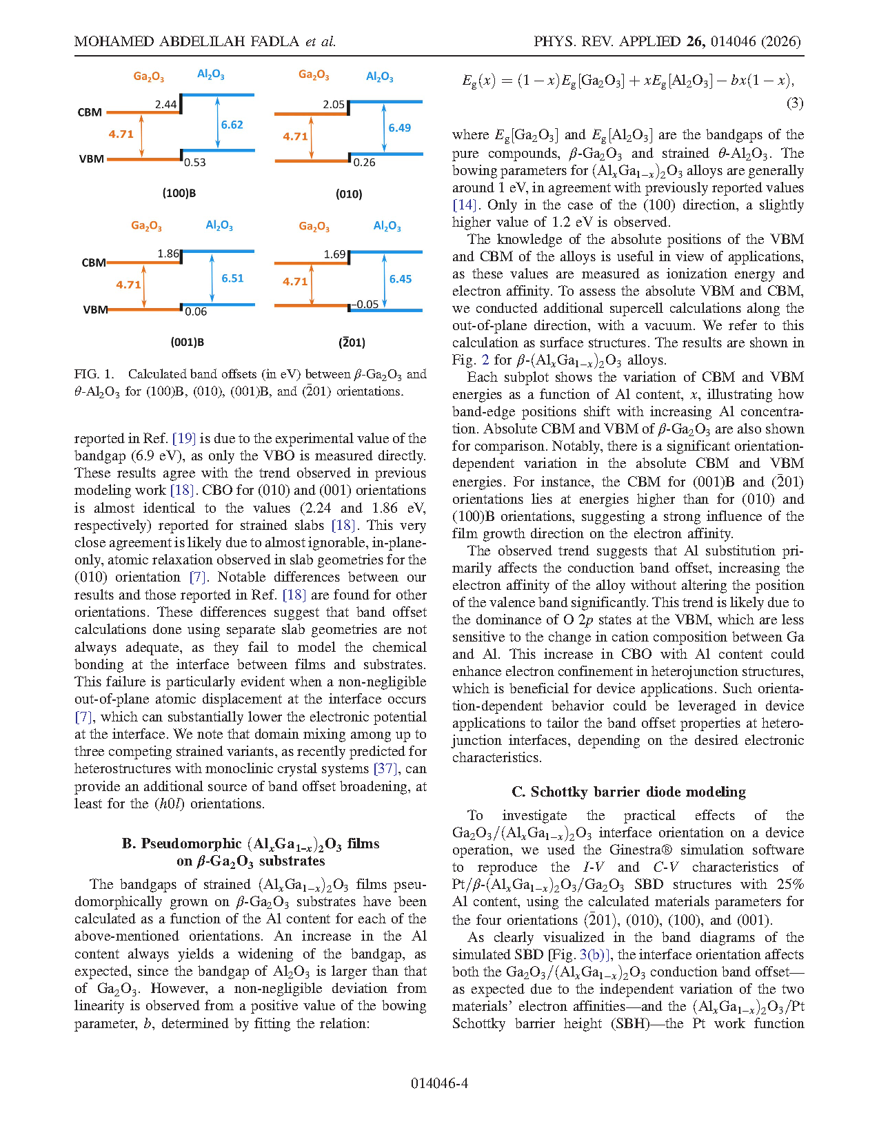
FIG. 1. Calculated band offsets (in eV) between β-Ga₂O₃ and θ-Al₂O₃ for (100)B, (010), (001)B, and (-201) orientations.
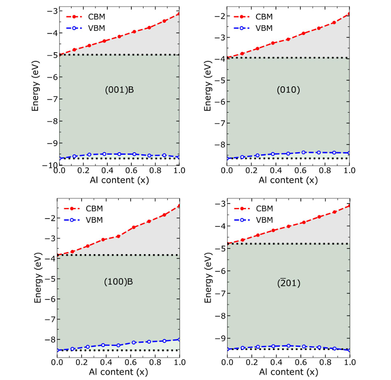
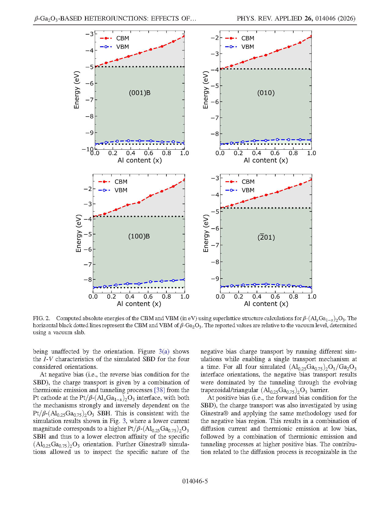
FIG. 2. Computed absolute energies of the CBM and VBM (in eV) using superlattice structure calculations for β-(AlₓGa₁₋ₓ)₂O₃. The horizontal black dotted lines represent the CBM and VBM of β-Ga₂O₃. The reported values are relative to the vacuum level, determined using a vacuum slab.
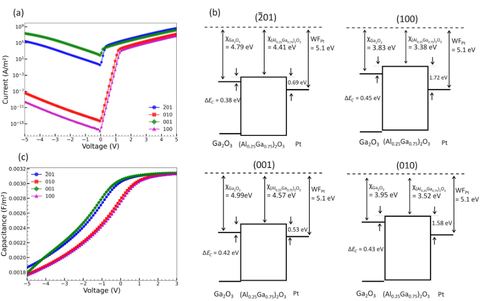
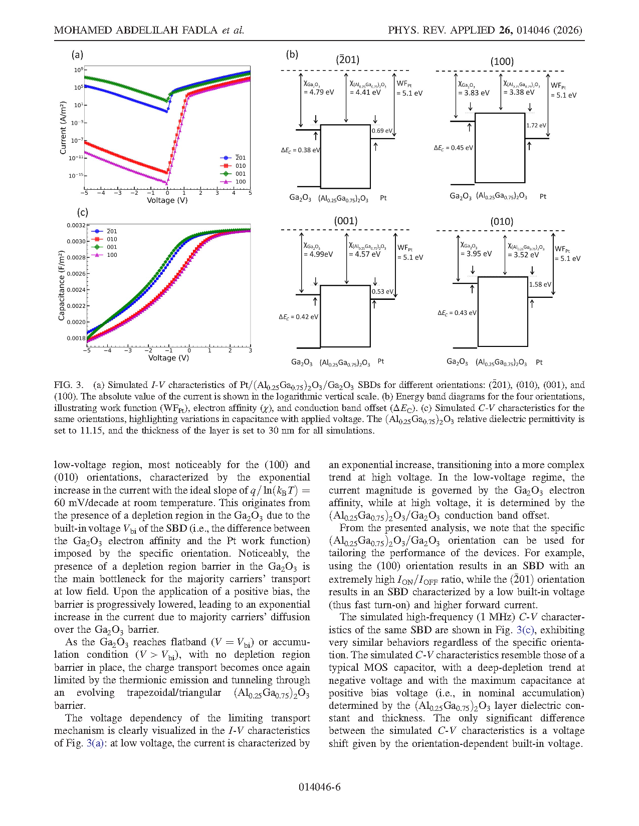
FIG. 3. (a) Simulated I-V characteristics of Pt/(Al₀.₂₅Ga₀.₇₅)₂O₃/Ga₂O₃ SBDs for different orientations: (-201), (010), (001), and (100). The absolute value of the current is shown in the logarithmic vertical scale. (b) Energy band diagrams for the four orientations, illustrating work function (WF_Pt), electron affinity (χ), and conduction band offset (ΔE_C). (c) Simulated C-V characteristics for the same orientations, highlighting variations in capacitance with applied voltage. The (Al₀.₂₅Ga₀.₇₅)₂O₃ relative dielectric permittivity is set to 11.15, and the thickness of the layer is set to 30 nm for all simulations.
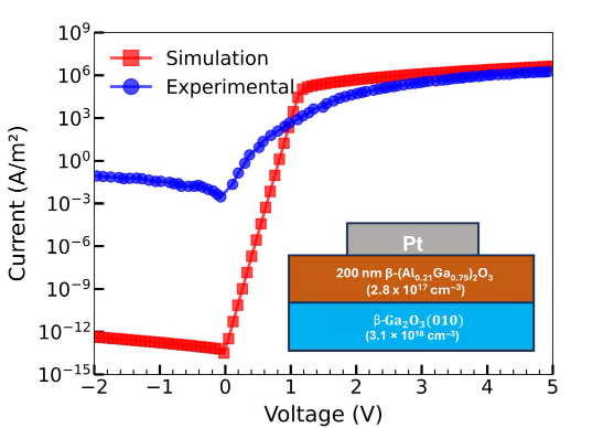
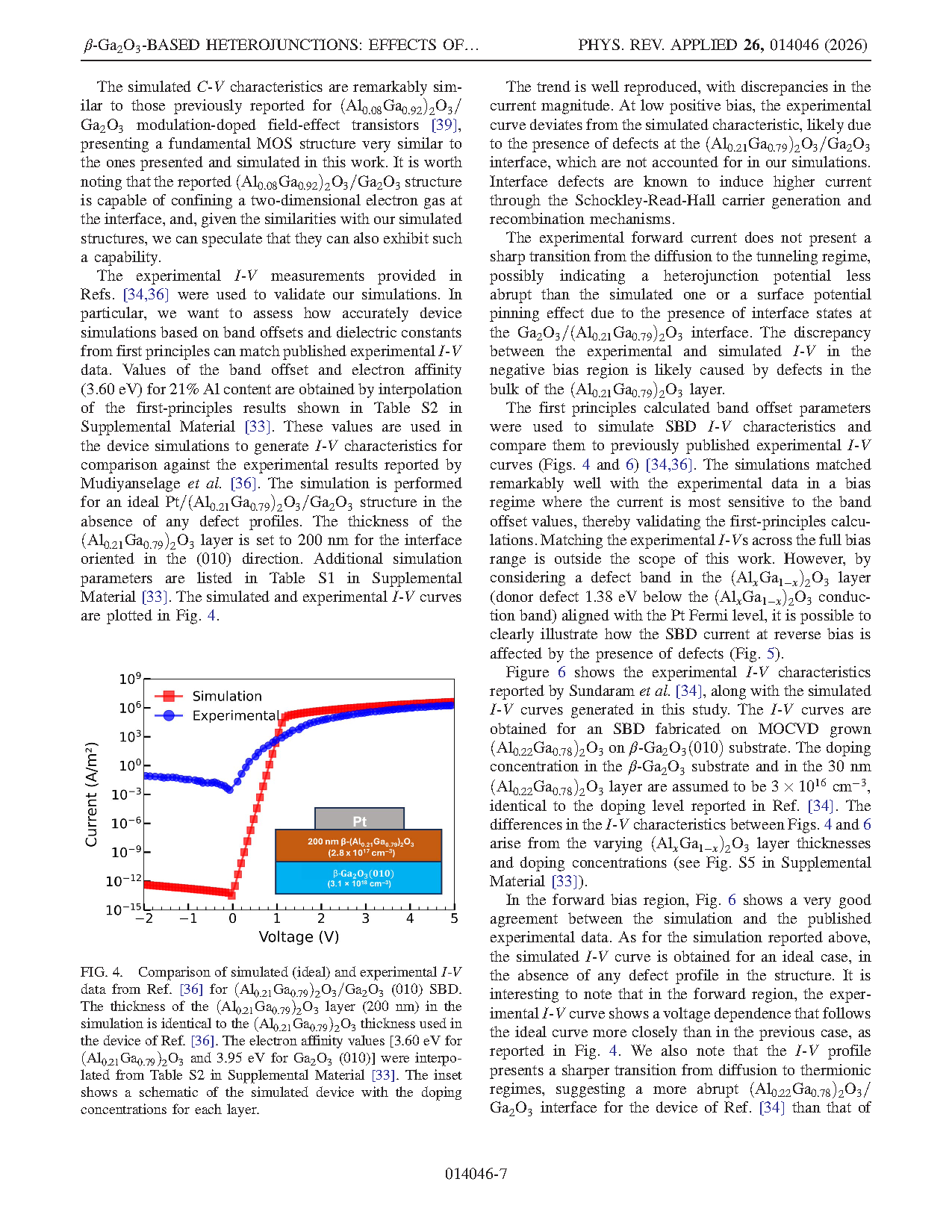
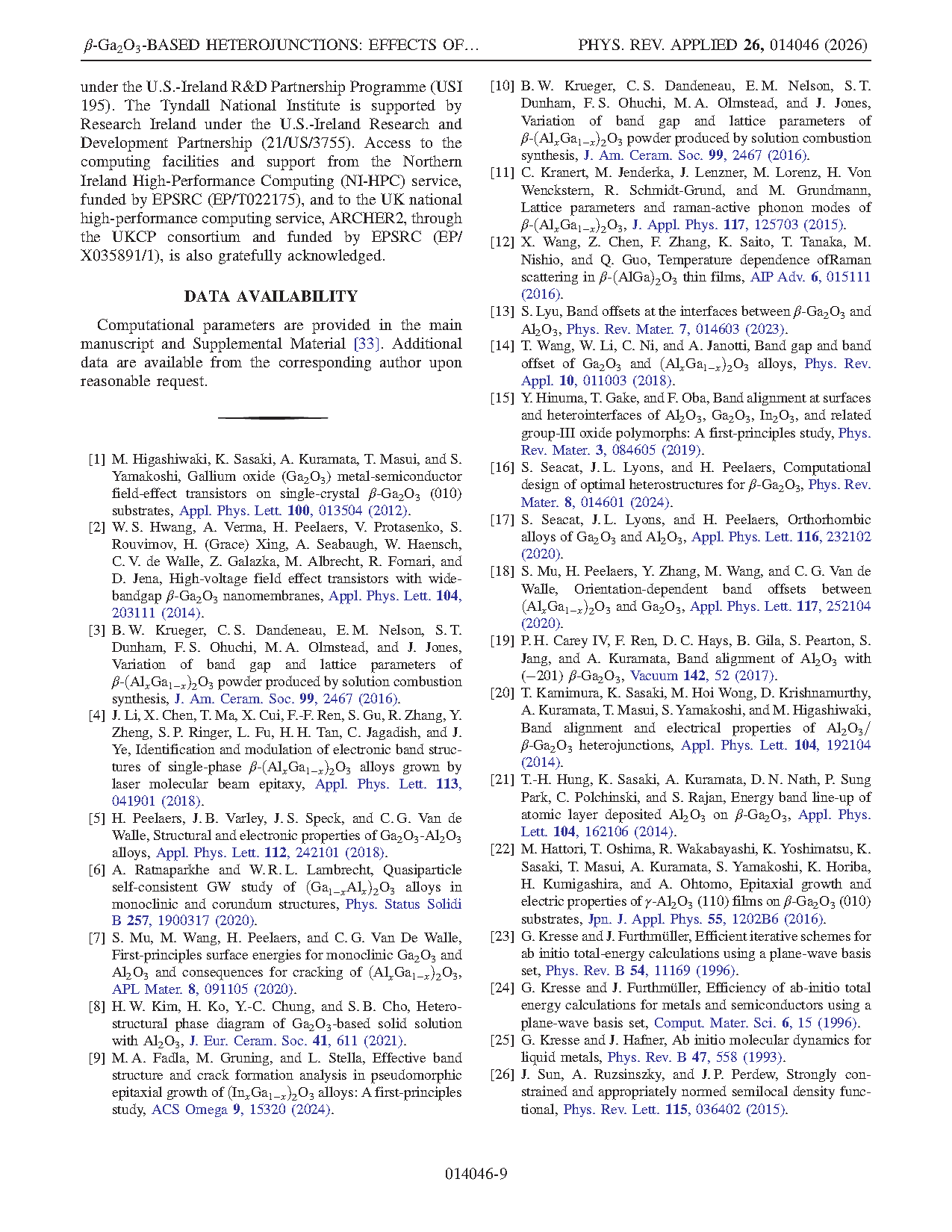
FIG. 4. Comparison of simulated (ideal) and experimental I-V data from Ref. [36] for (Al₀.₂₁Ga₀.₇₉)₂O₃/Ga₂O₃ (010) SBD. The thickness of the (Al₀.₂₁Ga₀.₇₉)₂O₃ layer (200 nm) in the simulation is identical to the (Al₀.₂₁Ga₀.₇₉)₂O₃ thickness used in the device of Ref. [36]. The electron affinity values [3.60 eV for (Al₀.₂₁Ga₀.₇₉)₂O₃ and 3.95 eV for Ga₂O₃ (010)] were interpolated from Table S2 in Supplemental Material [33]. The inset shows a schematic of the simulated device with the doping concentrations for each layer.
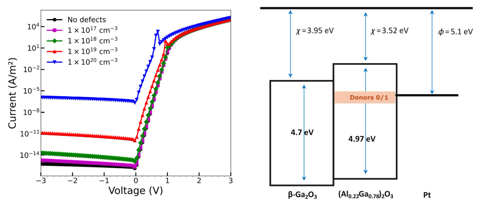
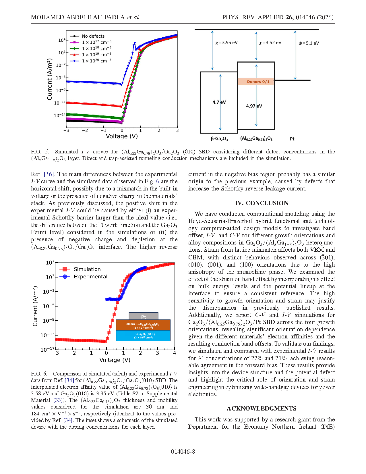
FIG. 5. Simulated I-V curves for (Al₀.₂₂Ga₀.₇₈)₂O₃/Ga₂O₃ (010) SBD considering different defect concentrations in the (AlₓGa₁₋ₓ)₂O₃ layer. Direct and trap-assisted tunneling conduction mechanisms are included in the simulation.
DOI:
10.1103/3vmk-vfcz
Instruction
Official Account

Cooperation
Top
