


A research team led by Academician Yue Hao and Prof. Genquan Han at Xidian University has published an article entitled “Reliability Enhancement of Ga₂O₃ Heterojunction Diodes Due to Space-Charge Modulation” in IEEE Transactions on Electron Devices.
Background
Ultrawide-bandgap β-Ga₂O₃, with a bandgap of approximately 4.9 eV and a theoretical critical electric field of about 8 MV/cm, is a promising material for next-generation ultrahigh-voltage and high-power electronics. p-NiO/n-Ga₂O₃ heterojunction diodes (HJDs) have attracted particular interest because of their strong leakage-current suppression and favorable high-temperature stability. As these devices are pushed toward higher voltage and current, however, long-term stability under high forward-bias stress has become a key reliability bottleneck. The physical origin of stress-induced degradation remains under debate, with proposed mechanisms involving interface dipoles, charge trapping, and gallium-vacancy (VGa) evolution. Clarifying the degradation, recovery, and self-stabilization processes of p-NiO/n-Ga₂O₃ HJDs under severe electrical stress is therefore essential for improving Ga₂O₃ power-device reliability.
Abstract
Long-term forward-bias stress activates a charge self-compensation mechanism, leading to anomalous recovery and performance enhancement. Under Vstress=8 V, short-term stress (≤ 50 s) causes clear performance degradation, whereas extending the stress duration to 200–1000 s restores the device characteristics and improves the ideality factor n from the pristine value of 1.08 to 1.03. This behavior indicates a stress-activated charge-compensation process rather than simple spontaneous recovery.
The enhancement originates from a two-stage self-compensating space-charge modulation involving electron trapping at VGa states and hole self-trapping at OI sites. SCLC, D-SIMS, C–V, and temperature-dependent Arrhenius analyses show that, during CT-I, deep acceptor-like VGa states capture electrons and generate negative space charge over an approximately 100 nm region in Ga₂O₃, with an extracted activation energy EA ≈ 0.16 eV. During CT-II, holes injected from p-NiO self-trap at adjacent OI sites, creating local positive charge that progressively neutralizes the previously accumulated negative space charge.
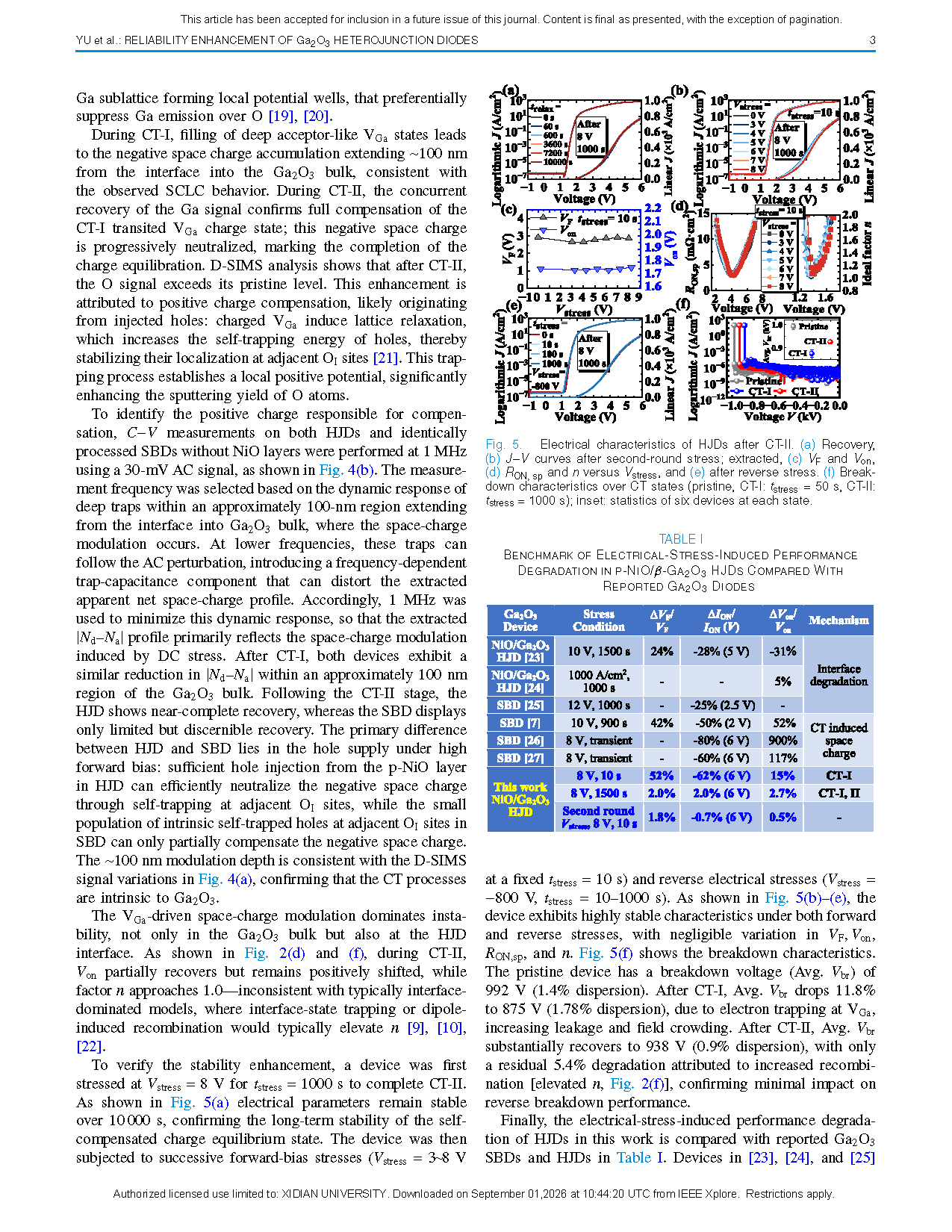
The self-compensated charge-equilibrium state exhibits high long-term stability while largely preserving reverse-blocking capability. After CT-II, the device remains stable during 10,000 s recovery and under a second round of forward and −800 V reverse stress. The average breakdown voltage decreases from 992 V in the pristine state to 875 V after CT-I, and then recovers to 938 V after CT-II, leaving only about 5.4% residual degradation.
Highlights
First identification of two sequential charge-trapping processes under sustained high forward stress. The work reveals a dynamic transition from initial degradation to long-term recovery and enhancement, characterized by two successive and opposing SCLC responses.
A VGa-related space-charge modulation mechanism involving self-trapped holes at adjacent OI sites is clarified. D-SIMS and C–V analyses reveal initial negative-charge accumulation at deep acceptor VGa states extending approximately 100 nm into Ga₂O₃, followed by neutralization through self-trapping of injected holes at adjacent OI sites.
Completion of both CT processes is shown to suppress degradation and markedly enhance long-term device reliability. The resulting self-compensated space-charge equilibrium effectively mitigates subsequent stress-induced degradation, revealing a new reliability mechanism in Ga₂O₃-based p-n heterojunctions and providing practical guidance for high-performance Ga₂O₃ power devices.
Conclusion
This study demonstrates that space-charge modulation through deep-level gallium-vacancy (VGa) states can significantly improve the long-term stability of p-NiO/n-Ga₂O₃ heterojunction diodes. Electrical characterization and D-SIMS analysis show that the enhancement originates from two sequential charge-trapping (CT) processes: negative charge first accumulates at deep VGa states within an approximately 100 nm region of the Ga₂O₃ bulk near the interface; subsequently, injected holes self-trap at adjacent oxygen sites (OI) under the influence of charged VGa states and progressively neutralize the previously accumulated negative space charge. Together, these processes establish a self-compensated VGa-related space-charge equilibrium near the interface, effectively suppressing stress-induced degradation and markedly improving device stability. This work reveals a new bias-induced reliability mechanism in Ga₂O₃-based p-n heterojunctions and provides a promising route for defect and space-charge engineering in reliable Ga₂O₃ power devices.
Project Support
This work was supported by the National Natural Science Foundation of China under Grants 62293522 and 62504032, and by the Key Program of the Shaanxi Provincial Department of Science and Technology Support under Grant 2024CY2-GJHX-81.
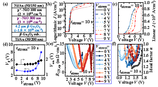
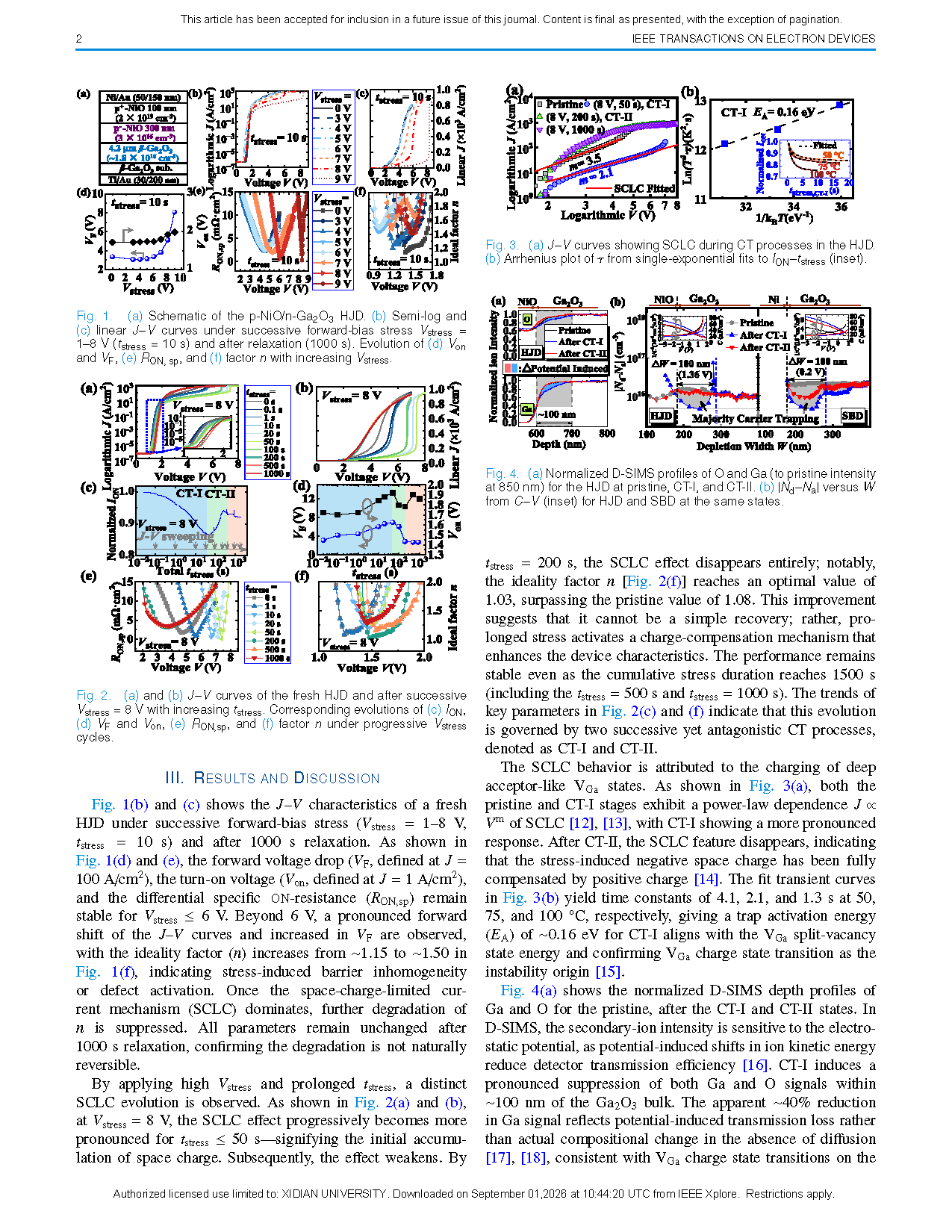
Fig. 1. (a) Schematic of the p-NiO/n-Ga₂O₃ HJD; (b)–(c) semi-log and linear J–V characteristics after successive forward-bias stress (1–8 V, tstress=10 s) and 1000 s relaxation; (d)–(f) evolution of Von, VF, RON,sp, and ideality factor n with Vstress.
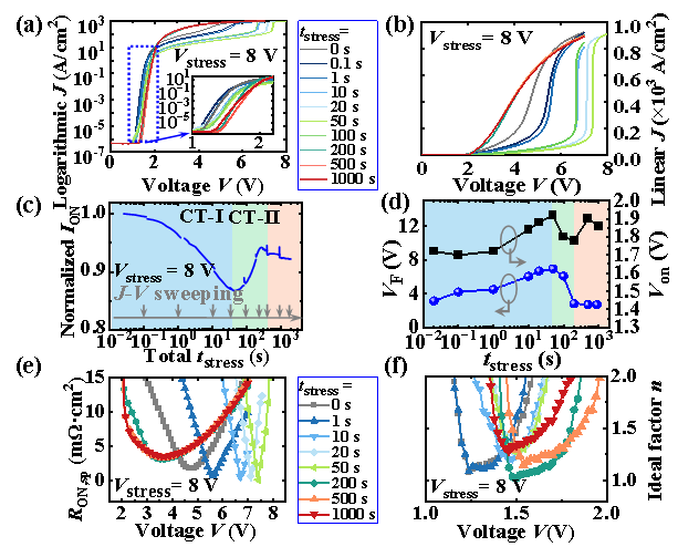
Fig. 2. (a)–(b) J–V evolution of the fresh HJD under Vstress=8 V with increasing stress time; (c)–(f) corresponding changes in ION, VF/Von, RON,sp, and ideality factor n, revealing the CT-I and CT-II stages.
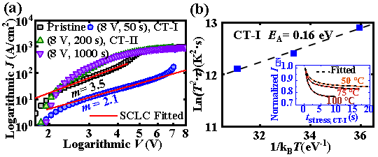
Fig. 3. (a) SCLC characteristics during the CT processes; (b) Arrhenius relation of the fitted CT-I time constant, yielding a trap activation energy EA ≈ 0.16 eV.
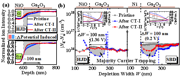
Fig. 4. (a) Normalized D-SIMS depth profiles of Ga and O in the HJD at pristine, CT-I, and CT-II states; (b) |Nd−Na| versus depletion width W extracted from 1 MHz C–V for HJD and SBD, showing an approximately 100 nm modulation depth and more complete CT-II recovery in the HJD.
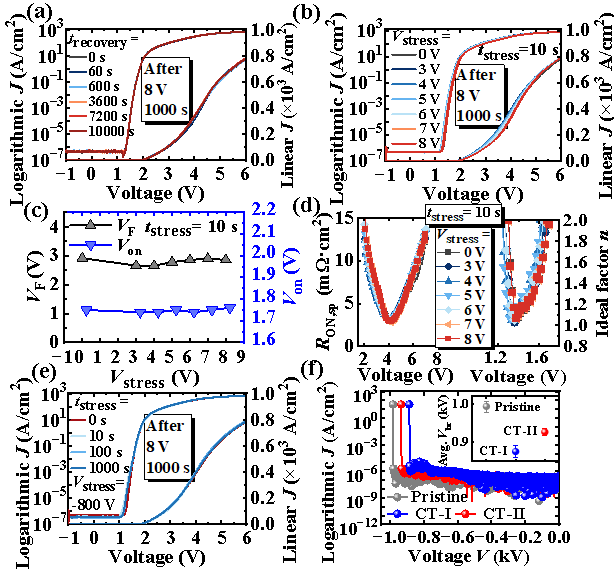
Fig. 5. Stability verification after CT-II: (a) 10,000 s recovery; (b)–(d) second-round forward-stress J–V characteristics and extracted VF/Von, RON,sp, and n; (e) −800 V reverse stress; (f) breakdown characteristics and statistics at pristine, CT-I, and CT-II states.
DOI:
10.1109/TED.2026.3723573
Instruction
Official Account

Cooperation
Top
