


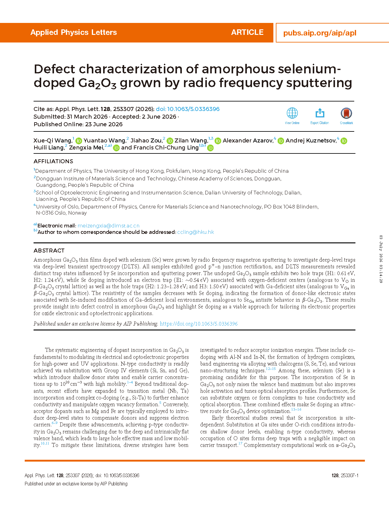
Researchers from The University of Hong Kong, Dongguan Institute of Materials Science and Technology, Dalian University of Technology & University of Oslo have published a paper titled "Defect characterization of amorphous selenium-doped Ga₂O₃ grown by radio frequency sputtering" in Applied Physics Letters.
Background
The doping engineering of Ga₂O₃ is fundamental to fabricate high-power and ultraviolet optoelectronic devices. Group IV dopants can achieve high n-type carrier concentration, while p-type conduction remains difficult due to deep intrinsic valence band and large hole effective mass. Traditional acceptor dopants such as Mg and Fe only introduce deep levels to compensate electrons. Alloying with chalcogen elements (S, Se, Te) can lift the valence band maximum and reduce acceptor ionization energy. Selenium (Se) doping shows outstanding merits: it can substitute O or Ga lattice sites to modulate band structure and tune optical absorption simultaneously.
Previous researches on Se-doped Ga₂O₃ mostly adopt ion implantation which induces severe lattice distortion. Radio frequency magnetron sputtering enables low-temperature growth of large-area amorphous Ga₂O₃ compatible with flexible substrates. However, deep-level traps induced by Se doping lack systematic quantitative characterization. Deep-level transient spectroscopy (DLTS) serves as a core method to analyze semiconductor defect states. Few studies systematically investigate how Se incorporation and sputtering power modulate electron and hole traps in amorphous Ga₂O₃. In this work, undoped and Se-doped amorphous Ga₂O₃ thin films are deposited under varied RF power. DLTS, XPS and SIMS are combined to distinguish deep traps originating from oxygen deficiency and gallium deficiency, revealing the intrinsic mechanism between Se doping, defect evolution and film resistivity. This work provides theoretical guidance for defect engineering of amorphous Ga₂O₃ optoelectronics.
Abstract
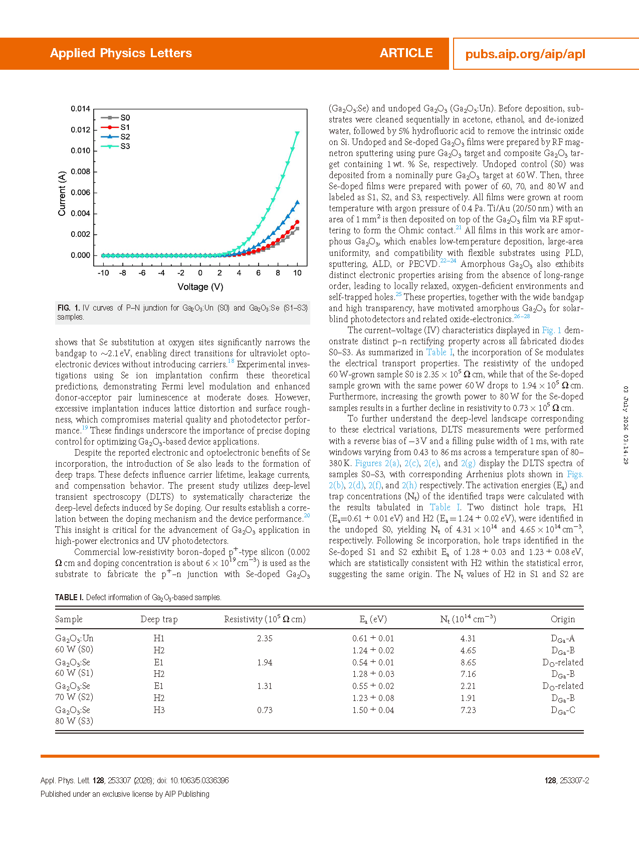
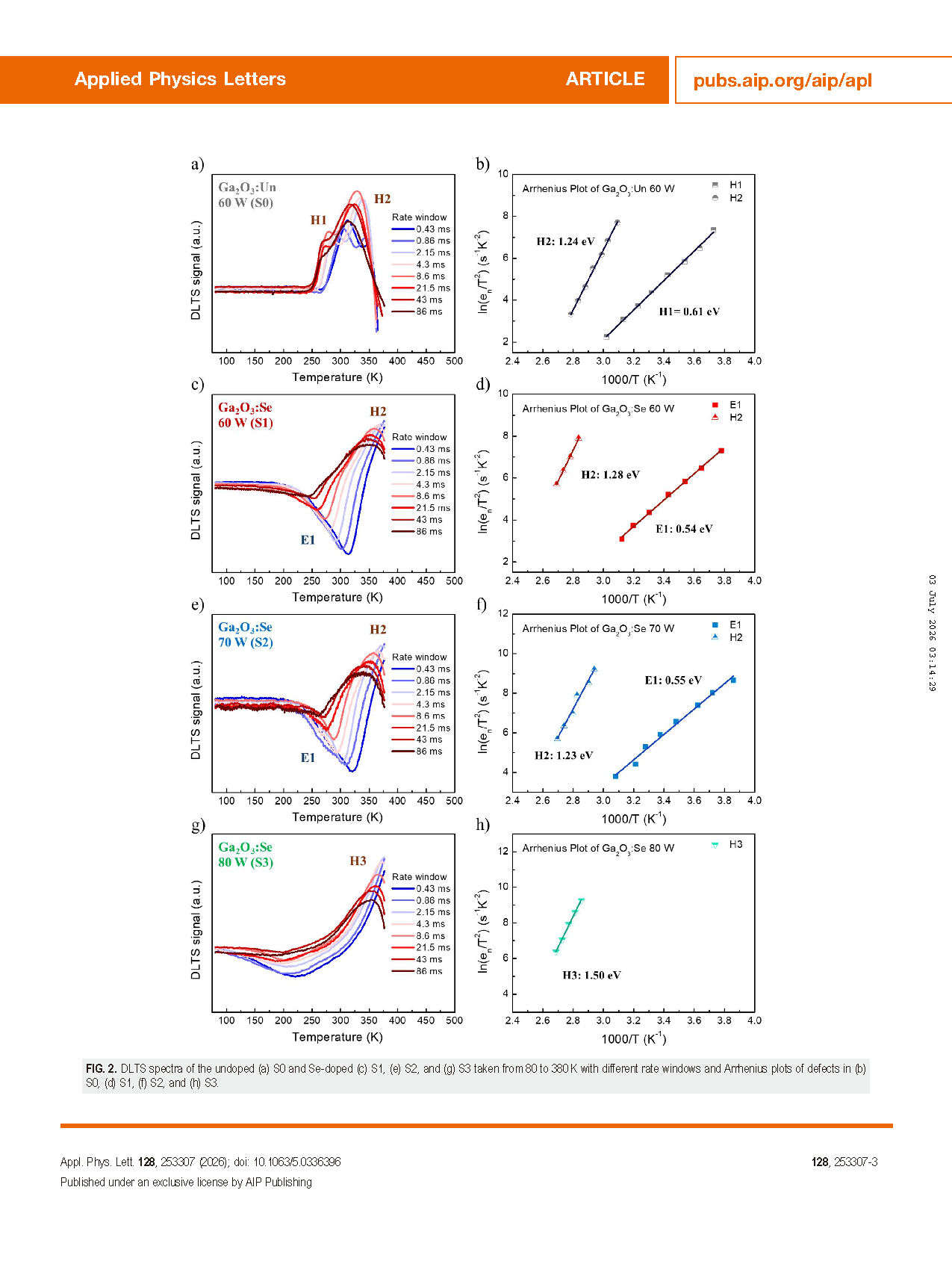
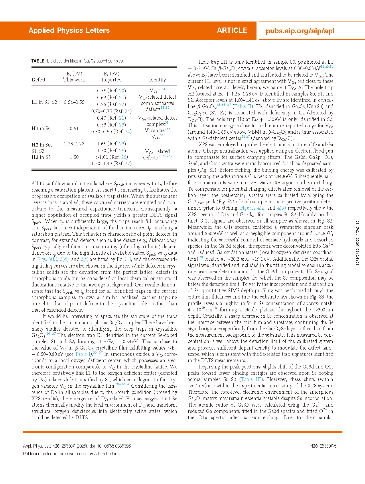
Amorphous Ga₂O₃ thin films doped with selenium (Se) were grown by radio frequency magnetron sputtering to investigate deep-level traps via deep-level transient spectroscopy (DLTS). All samples exhibited good p⁺–n junction rectification, and DLTS measurements revealed distinct trap states influenced by Se incorporation and sputtering power. The undoped Ga₂O₃ sample exhibits two hole traps (H1: 0.61 eV, H2: 1.24 eV), while Se doping introduced an electron trap (E1: ~ 0.54 eV) associated with oxygen-deficient centers (analogous to Vₒ in β-Ga₂O₃ crystal lattice) as well as the hole traps (H2: 1.23–1.28 eV; and H3: 1.50 eV) associated with Ga-deficient sites (analogous to VGa in β-Ga₂O₃ crystal lattice). The resistivity of the samples decreases with Se doping, indicating the formation of donor-like electronic states associated with Se-induced modification of Ga-deficient local environments, analogous to SeGa antisite behavior in β-Ga₂O₃. These results provide insight into defect control in amorphous Ga₂O₃ and highlight Se doping as a viable approach for tailoring its electronic properties for oxide electronic and optoelectronic applications.
Highlights
Large-area Se-doped amorphous Ga₂O₃is fabricated via low-temperature RF sputtering compatible with flexible substrates, and four samples under different sputtering powers are systematically compared for defect evolution;
DLTS quantitatively distinguishes oxygen-related electron trap E1 and multiple Ga-deficient hole traps H1/H2/H3 in undoped and Se-doped Ga₂O₃, with exact activation energy and trap concentration provided;
It is verified that Se doping generates donor-like local states and continuously reduces film resistivity, illustrating the modulation effect of Se_Ga antisite defects on energy levels;
XPS, SIMS, temperature-dependent DLTS and filling pulse variable measurements are integrated to build a complete correlation among sputtering power, Se concentration, defect species and electrical performance;
Low RF power induces oxygen vacancy electron traps while high power generates deeper Ga deficiency hole traps, offering experimental support for defect passivation and carrier tuning of amorphous Ga₂O₃.
Conclusion
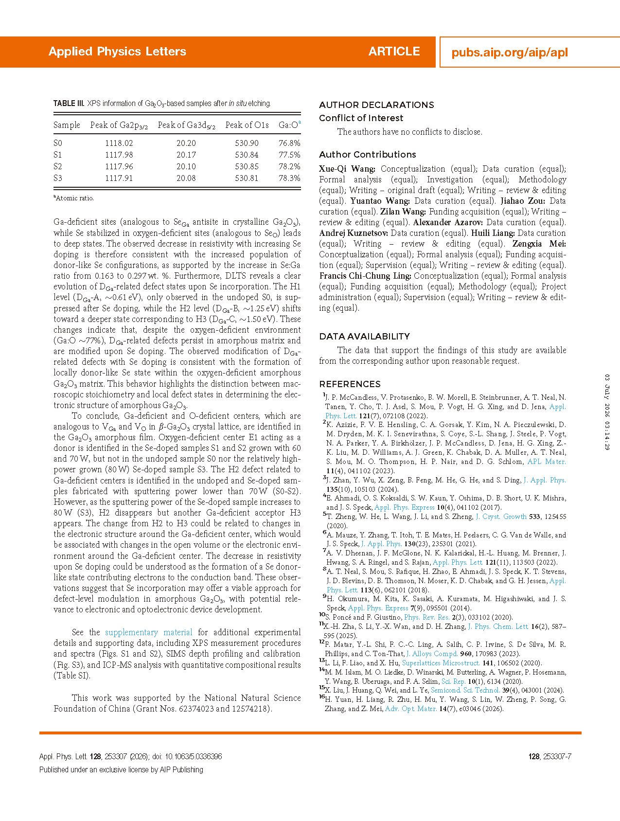
Selenium incorporation and sputtering power synergistically modulate the deep-level landscape of amorphous Ga₂O₃. Ga-deficient and O-deficient centers analogous to VGa and Vₒ in crystalline β-Ga₂O₃ are verified in amorphous Ga₂O₃ films. The electron trap E1 (~ 0.54 eV) related to oxygen deficiency only emerges in Se-doped samples S1 and S2, while the deeper hole trap H3 (1.50 eV) appears at high sputtering power of 80 W. H1 unique to undoped sample disappears after Se doping, and H2 shifts to deeper Ga-deficient trap H3 with rising sputtering power. The resistivity decreases with increased Se content owing to donor-like Se local configurations analogous to SeGa antisites. All traps follow point-defect carrier capture kinetics instead of extended dislocation defects. The combination of XPS, SIMS and DLTS confirms Se uniformly distributes inside films and modulates local Ga/O coordination environments to alter deep trap distribution. Se doping serves as an effective strategy to tailor defect states and electrical properties of amorphous Ga₂O₃ for oxide electronics and solar-blind optoelectronic devices.
Project Support
This work was supported by the National Natural Science Foundation of China (Grant Nos. 62374023 and 12574218).
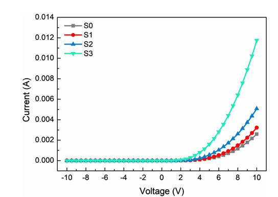
Figure 1 IV curves of p⁺–n junction for Ga₂O₃: Un (S0) and Ga₂O₃: Se (S1–S3) samples
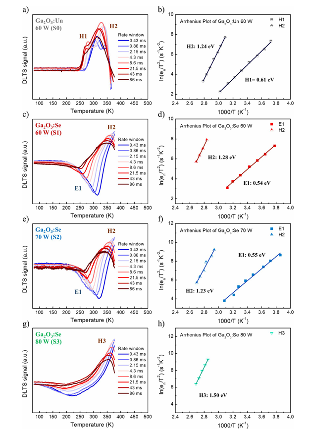
Figure 2 DLTS spectra of the undoped (a) S0 and Se-doped (c) S1, (e) S2, and (g) S3 taken from 80 to 380 K with different rate windows and Arrhenius plots of defects in (b) S0, (d) S1, (f) S2, and (h) S3
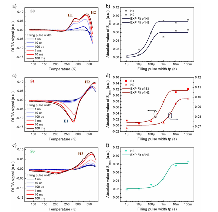
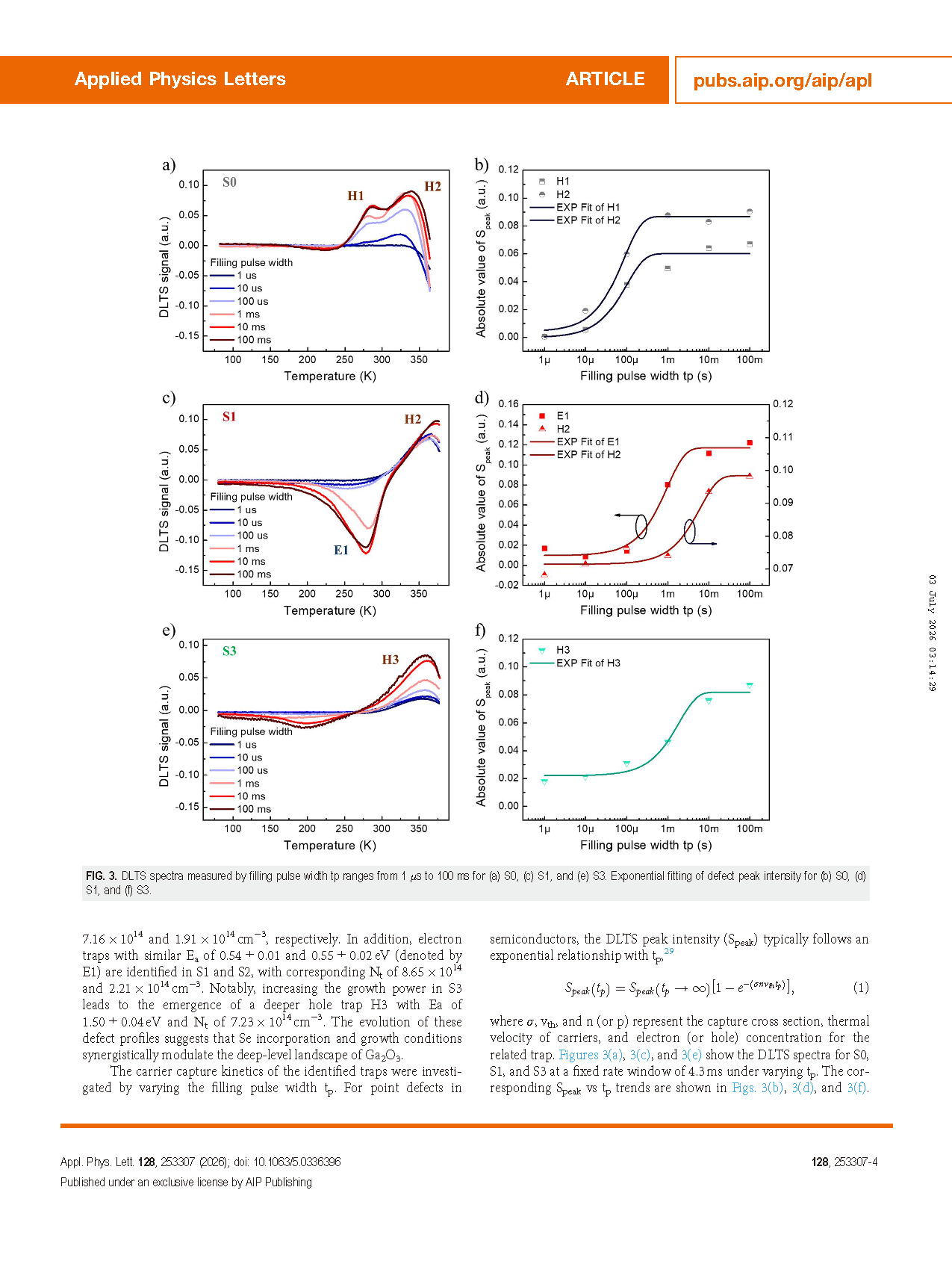
Figure 3 DLTS spectra measured by filling pulse width tₚ ranges from 1 μs to 100 ms for (a) S0, (c) S1, and (e) S3. Exponential fitting of defect peak intensity for (b) S0, (d) S1, and (f) S3
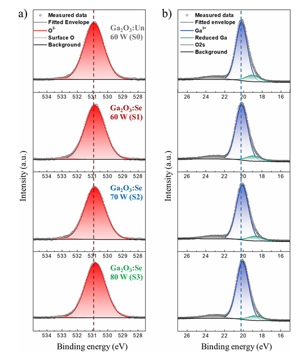
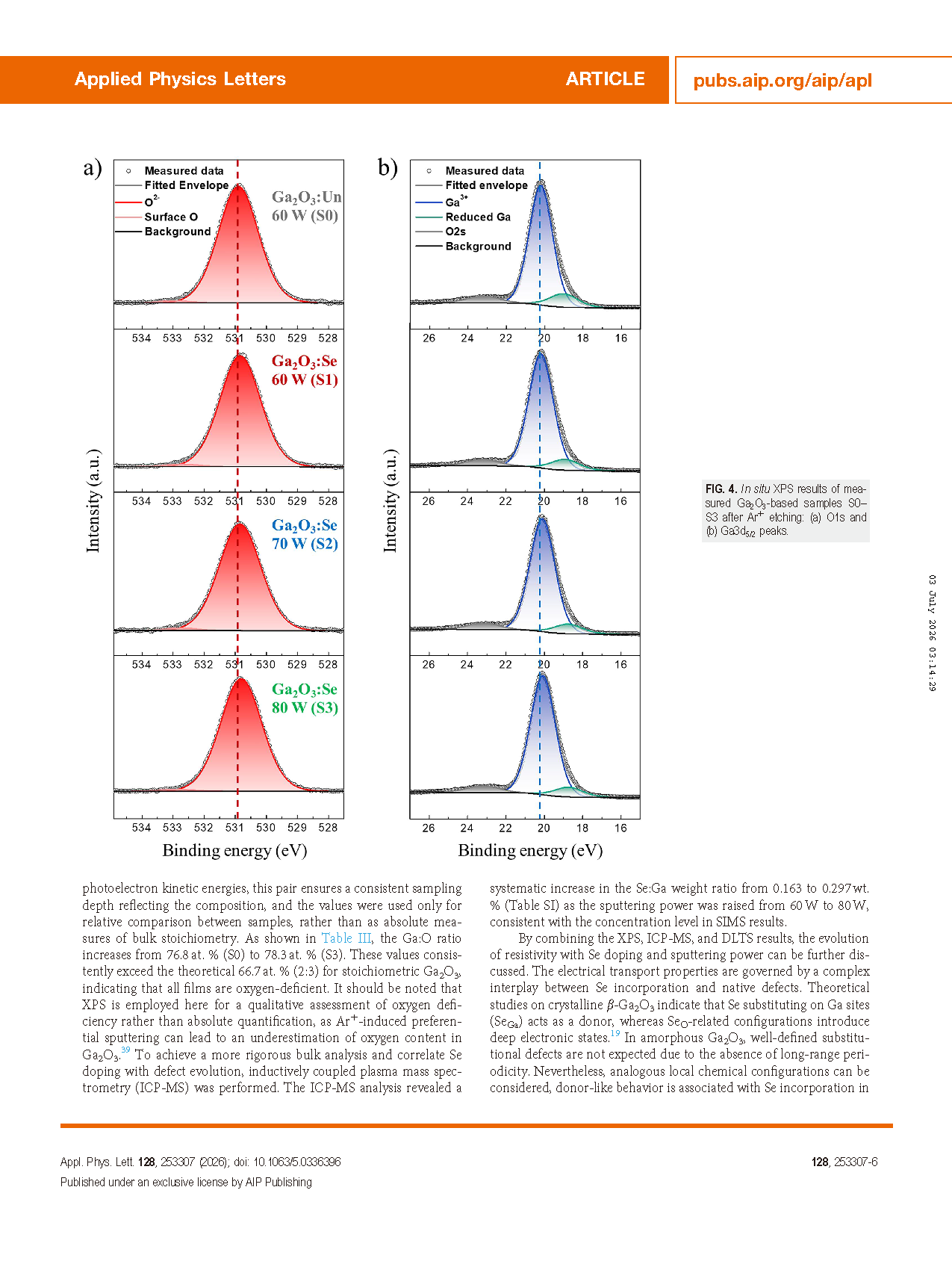
Figure 4 In situ XPS results of measured Ga₂O₃-based samples S0–S3 after Ar etching: (a) O 1s peaks, (b) Ga 3d₅/₂ peaks
DOI:
doi.org/10.1063/5.0336396
Instruction
Official Account

Cooperation
Top
