


In August 2026, experts, researchers, corporate representatives, and industry professionals from across the global gallium oxide community gathered in Maryland, USA, for the 6th International Workshop on Gallium Oxide and Related Materials (IWGO-6).
From crystal growth and epitaxy to device development and industrialization, the five-day conference brought together the latest advances from different regions around the world, offering a clear view of how gallium oxide is gradually moving beyond cutting-edge laboratory research toward a more defined path to commercialization.
But what a conference leaves behind is far more than presentations, posters, and data.
At IWGO-6, we spoke with experts, researchers, and industry representatives from different countries and regions, hearing their perspectives on technological progress, industrialization, and the future of the industry. These voices from the front lines of the field may offer a deeper understanding than technical performance metrics alone: Where does the global Ga₂O₃ industry stand today, and where is it heading next?
We have captured these perspectives as a snapshot of an industry entering its next stage of development.
Let’s start from IWGO-6 and hear the voices of the global Ga₂O₃ industry.
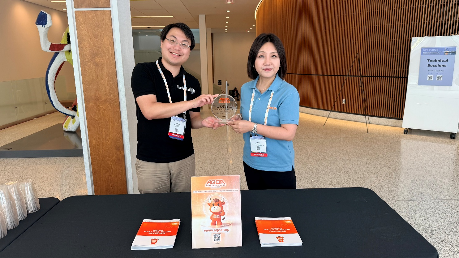
In this issue, we invited Dr. Dashun Zhou from NextGO Epi to share his insights into the future of gallium oxide, focusing on technological advances, device application exploration, and pathways toward commercialization.
1 A Growing Global Community
The most direct impression from IWGO 2026 was that the gallium oxide community is truly expanding.
The conference attracted a record‑high number of registered attendees, with 288 participants, marking the largest attendance in the history of IWGO. Compared with the 86 participants at the first IWGO held in Kyoto, the community has grown by more than threefold. This impressive turnout was achieved even with many researchers from mainland China unable to attend due to travel‑related restrictions.

2 Technology Trends: Materials Become More Refined, While Devices Flourish
Comparing with previous IWGO conferences, one trend has become increasingly evident: device-level validation work has surged, with a wide range of device architectures delivering promising high-voltage performance. In particular, vertical devices have essentially emerged as the future direction for gallium oxide power components.
On the materials side, discussions have become relatively more focused and in-depth. Researchers are shifting their attention toward the origins and impacts of various defects, while exploring novel growth techniques and crystal-plane selections to further reduce defect density and substrate costs. Among these developments, two approaches have attracted considerable attention: Japan’s NCT DG method and Japan’s FOX OCCG method. As breakthrough crucible-free crystal growth technologies, these approaches could, at least in theory, enable the production of 6-inch substrates at costs below $100. However, as with many emerging technologies, mass production still remains far off; as always, a timeline starting from at least five years should be expected.
Meanwhile, various companies have also showcased their progress in large-size substrates and epitaxial wafers (6-inch scale).
Overall, gallium oxide research has transitioned from the rapid-growth phase of diverse exploration (2012-2022) into a more stable development stage. Fundamental material studies have largely established a foundation, and the community is converging by consensus around specific technology routes with mass-production potential. For substrates, EFG and VB methods have become the dominant pathways, while epitaxial growth is mainly focused on MOCVD and HVPE technologies.
Beyond this relatively mature technological framework, remarkable measurement results for Al-alloy-based 2DEG and continued progress in crucible-free crystal growth technologies are adding new possibilities for gallium oxide’s future cost and application scope.
3 The Crystal Plane Debate: Pursuing Perfection or Advancing Pragmatically
If I were to summarize the key discussions from IWGO 2026 with two questions, they would be: Which crystal plane is suitable? And when will reliable gallium oxide devices become available?
To further improve device performance and epitaxial quality, the community has begun expanding its focus beyond the traditionally dominant (001) and (010) crystal planes toward previously less-explored orientations such as (011), (-102), and (100). I welcome this growing interest, as it reflects the continued exploration and maturity of the field. However, I also worry that the discussion may shift away from the most critical priorities.
For researchers and engineers working on epitaxy and device development, substrate yield and future cost are ultimately far more important than the choice of crystal plane itself. Rather than spending another decade searching for a “perfect” crystal plane — assuming such a plane even exists — it may be more practical to establish a reliable device fabrication process based on a mature, cost-effective substrate orientation.
At its current stage, gallium oxide urgently needs a reliable device with distinct performance advantages to prove its value to the market.
During the conference, several semiconductor professionals who had previously worked extensively on SiC pointed out that SiC delivers nearly a hundred-fold improvement over silicon in comprehensive high-voltage performance (breakdown voltage and on-resistance), whereas gallium oxide may offer at most a ten-fold improvement over SiC.
This raises a fundamental question: Is this performance margin sufficient to justify large-scale investment and sustained industry efforts?
As the saying goes, “Do not undertake reform unless benefits are hundredfold.” This may be one of the most important questions that gallium oxide practitioners need to address as soon as possible.
4 Roundtable Consensus: Focusing on Core Advantages and the China Factor
During the roundtable discussion on the conference’s third evening, invited speakers and attendees reached an important consensus on gallium-oxide’s prospects in comparison with SiC: rather than spreading efforts thin, the gallium-oxide community should concentrate on developing reliable devices that can truly deliver its breakdown electric field of 8 MV/cm (or at least approach this value). This is its sole and most dependable competitive advantage.
As for pricing: gallium oxide still boasts negligible price advantages over silicon carbide. Furthermore, gallium oxide’s genuine cost advantage ought to materialize at the system level, instead of through simple price comparisons of individual die. Drawing on his two-decade-long experience in the SiC industry, Dr. Veliadis from Power America predicts that the first mature gallium-oxide product will likely be a 3.3 kV SBD device, which will serve as the starting point for further advancement toward 20 kV.
Due to the conference venue, most speakers presented perspectives rooted in European and American viewpoints. Fortunately, Prof. Wen-Hai Huang was among the panelists and brought up “the elephant in the room” — China. Compared with previous editions of IWGO, this year saw participation from representatives of global heavyweights including Mitsubishi and Infineon. This can be partly attributed to the momentum of China, the world’s largest power-semiconductor market.
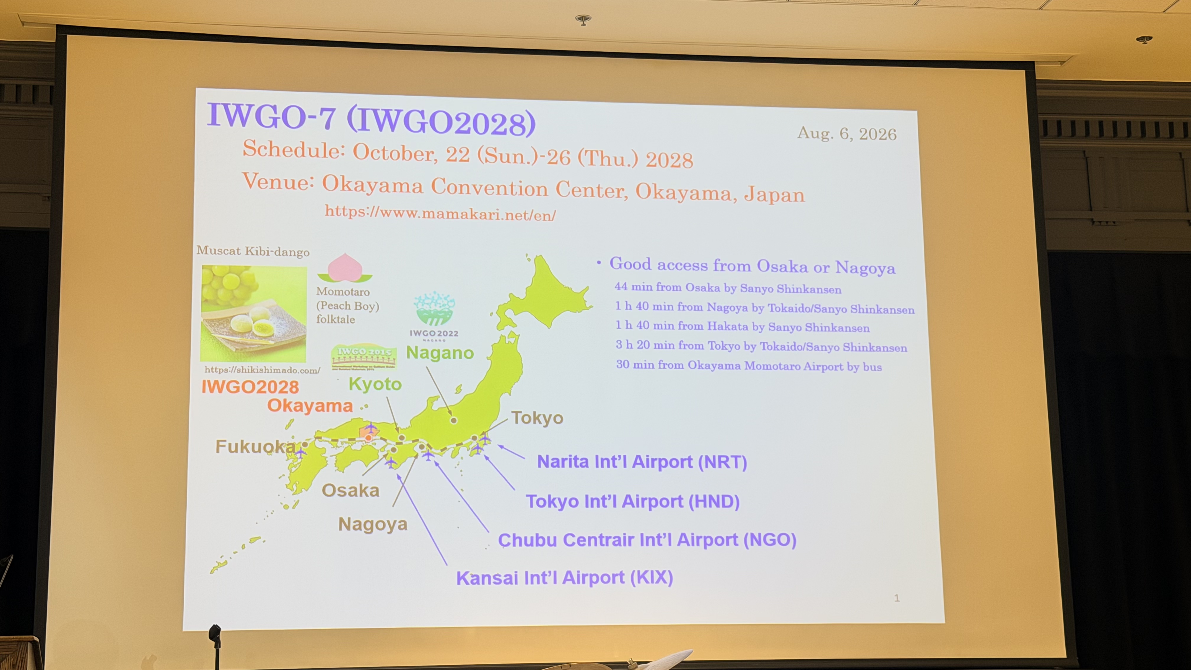
China has pulled far ahead of Europe, the United States and other regions in industrialization progress. It holds an order-of-magnitude lead over other countries both in the number of enterprises and supply-chain completeness. For better or worse, this competitive strength remained largely hidden from view because of where the conference was held. Prof. Huang’s remarks reminded the audience that any projection for gallium-oxide’s future would be incomplete without incorporating China as a key variable. In closing, the organizers expressed their hope for joint efforts across the global gallium-oxide community in this direction, looking forward to gallium-oxide delivering remarkable achievements at the next IWGO 2028 in Okayama, Japan.
5 From the Laboratory to the Industrial Frontline: Four Questions from SEMICON Taiwan
If IWGO showcased the possibilities of gallium oxide from a research perspective, then SEMICON Taiwan a few weeks later offered a view of how the same technology is being evaluated in the industrial landscape.
SEMICON Taiwan has long been a major showcase for the conventional semiconductor industry. Over the past two years, driven by the rapid growth of AI technologies, the scale of exhibitors and attendance reached new highs. A wide range of AI-related technologies took center stage, covering everything from silicon photonics to data center systems.
With the increasing demand for high-voltage power systems in data centers, gallium oxide, as a candidate material for next-generation power devices, also began to appear at the booths of several material and equipment companies this year, including Japan-based NCT and FOX. Although it remains a supporting role rather than a main focus, gallium oxide is at least no longer a term that requires a lengthy introduction.
Interestingly, the questions raised on the industrial floor were almost entirely different from those discussed at IWGO. Topics that attracted extensive academic debate—such as crystal orientation selection and defect mechanisms—were rarely brought up here. Instead, industry participants focused on four highly practical questions:
What is the yield?
What is the cost?
When can it enter mass production?
Who is using it today?
These four questions happen to represent the areas where gallium oxide currently faces its greatest challenges.
Such a gap is not surprising—it is a hurdle that every emerging material must overcome when transitioning from the laboratory to manufacturing. However, experiencing both environments firsthand makes the contrast particularly clear: the distance between demonstrating technical potential and achieving industrial adoption remains a critical stage in gallium oxide’s development.
6 Conclusion: The Window to Turn “Possibility” into “Reality”
From IWGO to SEMICON Taiwan, traveling across the two ends of the technology and industry spectrum within just a few weeks led me to a rather straightforward conclusion: the technical potential of gallium oxide has already been demonstrated extensively. What needs to be proven next is its industrial viability—a device with controllable yield, acceptable cost, and clearly defined performance advantages.
With two years remaining until the next IWGO, which will be held in Okayama, Japan, in 2028, this period may represent a critical window for transforming gallium oxide from a “possibility” into a “practical reality.”
NextGO Epi Company Introduction
Bringing Gallium Oxide to Mass Production — Europe's First Gallium Oxide Epitaxy Technology Company
About NextGO Epi

Gallium oxide (Ga₂O₃) is regarded as one of the most promising fourth-generation wide-bandgap semiconductor materials following silicon carbide (SiC) and gallium nitride (GaN). While it delivers notable theoretical performance advantages, its industrialization has long been bottlenecked by epitaxy: how to fabricate large-size wafers with uniform thickness while preserving high crystal quality remains a shared challenge for material teams worldwide. The founding of NextGO Epi is aimed squarely at solving this problem.
Headquartered within the campus of the Leibniz-Institut für Kristallzüchtung (IKZ, Leibniz Institute for Crystal Growth) in Berlin, Germany, the company was founded in 2025 by Dr. Dashun Zhou, Dr. Andreas Popp and Dr. Andreas Fiedler. It is a technology spin-off incubated by IKZ.
All three co-founders hail from one of the world’s earliest teams conducting gallium-oxide epitaxy research and publishing pioneering relevant results. Years of accumulated process know-how have been converted into a cross-border patent portfolio, underpinning the company’s independent technological capabilities in both homoepitaxy and heteroepitaxy.
Technology Roadmap: Why MOCVD?
Currently, the two mainstream gallium-oxide epitaxy methods in the industry each have inherent limitations. HVPE features fast growth rates, yet it is difficult to balance uniformity and doping control simultaneously. MBE achieves high precision, but is constrained by throughput and wafer size, making it uneconomical for mass production.
NextGO Epi selects MOCVD (Metal-Organic Chemical Vapor Deposition) as its core process route precisely for its balance between large-size uniform growth and process controllability — this is the only technical path capable of satisfying power-semiconductor industry requirements for thickness accuracy, within-wafer uniformity and batch-to-batch consistency all at once.
Building on this foundation, NextGO Epi has further developed its globally exclusive real-time monitoring technology for epitaxial growth. It enables key parameters during growth to be captured and adjusted on-the-fly, substantially improving yield and batch stability. This is one of the core competitive advantages that differentiates the company from other epitaxy suppliers.
In terms of crystal-orientation selection, NextGO Epi masters gallium-oxide epitaxy technologies for both (100) and (010) orientations. It can deliver products of corresponding crystal orientations according to device architectures and application requirements. The products combine good cleavability and low defect density, affording customers greater flexibility in device design.
Product Portfolio: Scaling from Small Coupons to Six-Inch Wafers
NextGO Epi’s product line covers 10 mm × 10 mm small coupons, 2-inch and 4-inch wafers, available in both (100) and (010) crystal orientations. Graded product supply matches customer needs across early-stage material evaluation, pilot-scale scaling and mass-production adoption.
Small coupons, 2-inch and 4-inch epitaxial wafers are already in full mass-production supply. 6-inch epitaxial wafers have entered pilot production and will be ramped up gradually in response to market demand, completing the full size chain from laboratory evaluation to production-line deployment step-by-step.
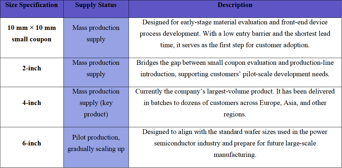
To date, NextGO Epi has delivered products to dozens of customers mainly in Europe and extending to Asia, including power-device R&D institutes, material-validation laboratories and production-line customers. The product lineup and production capacity keep expanding continuously.
Industrial Collaboration: Deepening Roots in Europe and Connecting the Gallium Oxide Value Chain
Materials are only the first step. NextGO Epi attaches greater importance to stitching together the full gallium-oxide value chain.
Upstream, the company maintains close partnerships with leading suppliers including Hangzhou Garen Semiconductor, Hangzhou Fujia Gallium, Suzhou Gahe Gallium Oxide and Japan’s NCT, consolidating the supply base for equipment and raw materials.
Downstream, with its base in Berlin, the company actively cooperates with power-semiconductor and end-application partners across Europe such as Spain, Italy, Türkiye and France to jointly validate device performance, enabling gallium-oxide technologies to take root and deliver results within the European industrial ecosystem.
Recognition from the Capital Market
In July 2026, NextGO Epi closed its €2 M pre-Seed financing round, led by German venture-capital firm Vireo Ventures, with participation from European institutions including IBB Ventures (under Investitionsbank Berlin), alongside angel investors. This financing provides solid financial support for the company’s technology development and capacity expansion, and also marks recognition from European capital markets toward gallium-oxide’s commercialization path.
Next Steps
Having secured its foothold in the European market, NextGO Epi’s next priority is to fully mature and solidify its 6-inch epitaxy capability. Leveraging its geographic advantage, the company will keep expanding partners and customers in more countries, so that MOCVD-based gallium-oxide epitaxy becomes a trustworthy mass-production option for the power-semiconductor industry. Together with global partners, we look forward to witnessing the turning point for gallium-oxide industry: moving from laboratory R&D toward large-scale application.
Instruction
Official Account

Cooperation
Top
