


Researchers from the University of Electronic Science and Technology of China and China Resources Microelectronics Ltd. have published a paper titled "A New Concept β-Ga₂O₃ Device: Lateral β-Ga₂O₃/p-NiO Heterojunction IGBT with Improved On state Current Density" in Semiconductor Science and Technology.
Background
Monoclinic β-Ga₂O₃ is an ultra-wide bandgap semiconductor with a bandgap of 4.8-4.9 eV and a theoretical breakdown field up to 8 MV/cm, which shows great promise for high voltage power electronics. Various β-Ga₂O₃ MOSFET devices have been reported with kilovolt class breakdown voltages. However, as unipolar devices, β-Ga₂O₃ MOSFETs suffer from high on resistance under high voltage operation. Owing to the lack of feasible p type doping, the performance of β-Ga₂O₃ unipolar devices is far below its theoretical limit. Heterogeneous integration of p-type NiO with β-Ga₂O₃ enables efficient hole injection into drift region to realize bipolar conduction and conductivity modulation, which provides a feasible route to break the performance limitation of unipolar devices. Previous works mainly focus on heterojunction diodes, while the design and simulation of β-Ga₂O₃ IGBT remain rarely reported. In this work, a novel lateral β-Ga₂O₃/p-NiO heterojunction IGBT structure is proposed. Combining p-NiO anode hole injection, nitrogen implanted current blocking layer and superjunction like drift region, TCAD simulations are performed to investigate device mechanism and performance, offering design references for high-performance β-Ga₂O₃ power IGBT development.
Abstract
A new concept beta gallium oxide (β-Ga₂O₃) device—lateral β-Ga₂O₃/p-NiO heterojunction insulated gate bipolar transistor (IGBT) is proposed and investigated for the first time via technology computer aided design (TCAD) simulations. The n-Ga₂O₃/p-NiO heterojunction in the anode region facilitates efficient hole injection and strong conductivity modulation, thereby effectively enhancing the on state current density. Nitrogen implantation (NI) beneath the gate is incorporated to form a current blocking layer, which enables reliable enhancement mode (E mode) operation. In addition, the p-NiO layer introduced above the drift region, together with the n-Ga₂O₃ region and the overlying Al₂O₃ layer, forms a superjunction like drift region, thereby optimizing the electric field distribution during reverse blocking condition, leading to a significantly improved breakdown voltage (Vbr). Simulation results show that with a drift region length (Ldrift) of 30 μm, the proposed IGBT achieves a breakdown voltage of 15.2 kV and exhibits excellent on state conduction characteristics. At a gate voltage of 15 V and an on-state voltage of 10 V, the on state current density of the proposed IGBT is nearly 3 times that of the β-Ga₂O₃ metal oxide semiconductor field effect transistor (MOSFET) with the same drift region length and doping concentration. In summary, this work offers a promising pathway and valuable guidance for the development of high-performance β-Ga₂O₃ IGBT devices.
Highlights
A novel lateral β-Ga₂O₃/p-NiO heterojunction IGBT architecture is proposed for the first time. Multiple designs including p-NiO anode hole injection, nitrogen implanted current blocking layer under gate and superjunction like drift region are integrated, and device mechanism is verified via TCAD simulation.
The p-NiO anode realizes efficient hole injection and conductivity modulation. With 30 μm drift region length, the on state current density is nearly 3 times higher than MOSFET under identical conditions, greatly improving conduction capability. ③ The p-NiO/Al₂O₃/n-Ga₂O₃ forms superjunction like drift region to optimize reverse blocking electric field distribution, and a high breakdown voltage of 15.2 kV is obtained in simulation.
Systematic investigations are carried out on influences of p-NiO doping concentration, length, anode p+ doping, hole lifetime, interface trap charge and electro thermal effect on static and switching performance, revealing physical limiting factors of the device.
Benchmark comparisons with reported β-Ga₂O₃ power devices are performed. The proposed lateral IGBT achieves a power figure of merit of 6.07 GW/cm2, offering a new solution for lateral high voltage gallium oxide devices.
Conclusion
A novel lateral β-Ga₂O₃/p-NiO heterojunction IGBT is proposed and investigated herein. The p-NiO heterojunction realizes efficient hole injection and conductivity modulation to reduce conduction loss, while the NI forms a current blocking layer for reliable E mode operation. The p-NiO layer optimizes charge balance and electric field distribution, greatly improving Vbr. The device exhibits a Vbr of 15.2 kV and a PFOM of 6.07 GW/cm2. This work provides a feasible approach and valuable guidance for the development of high-performance high voltage β-Ga₂O₃ power devices.
Project Support
This work was supported in part by the Central Guiding Local Science and Technology Development Special Project of Sichuan (2024ZYD0310).
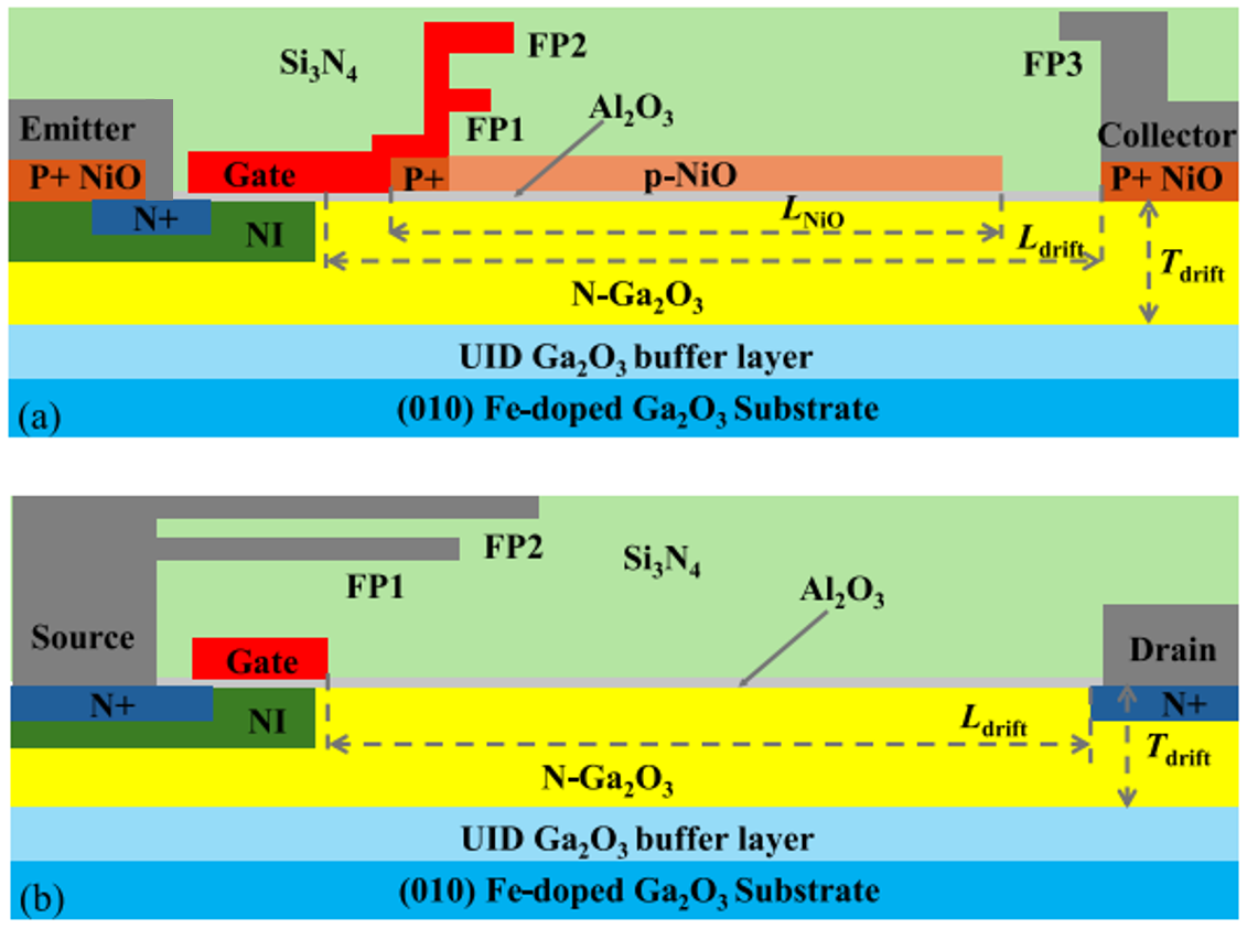
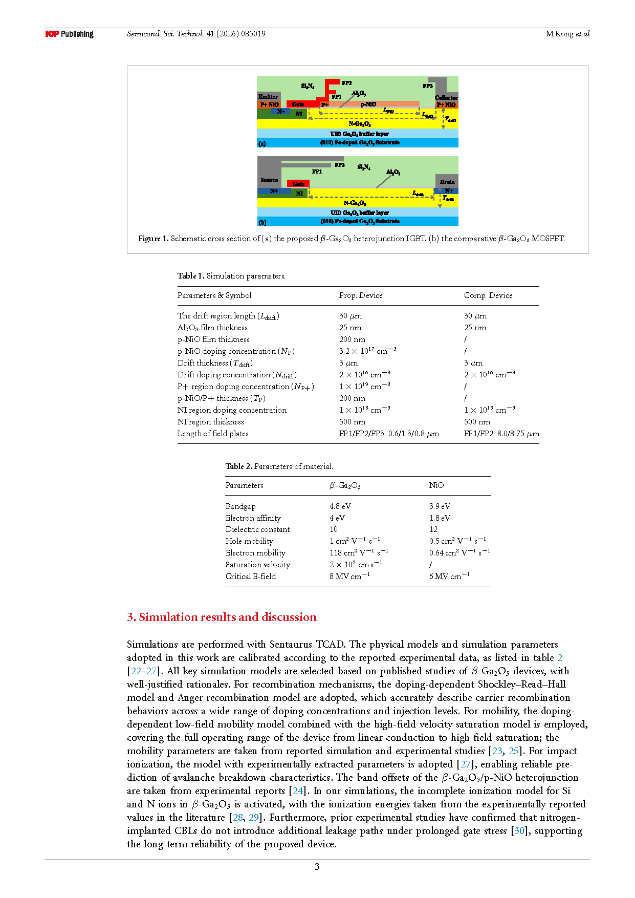
Figure 1. Schematic cross section of (a) the proposed β-Ga₂O₃ heterojunction IGBT. (b) the comparative β-Ga₂O₃ MOSFET.
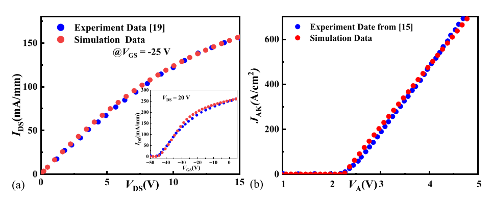
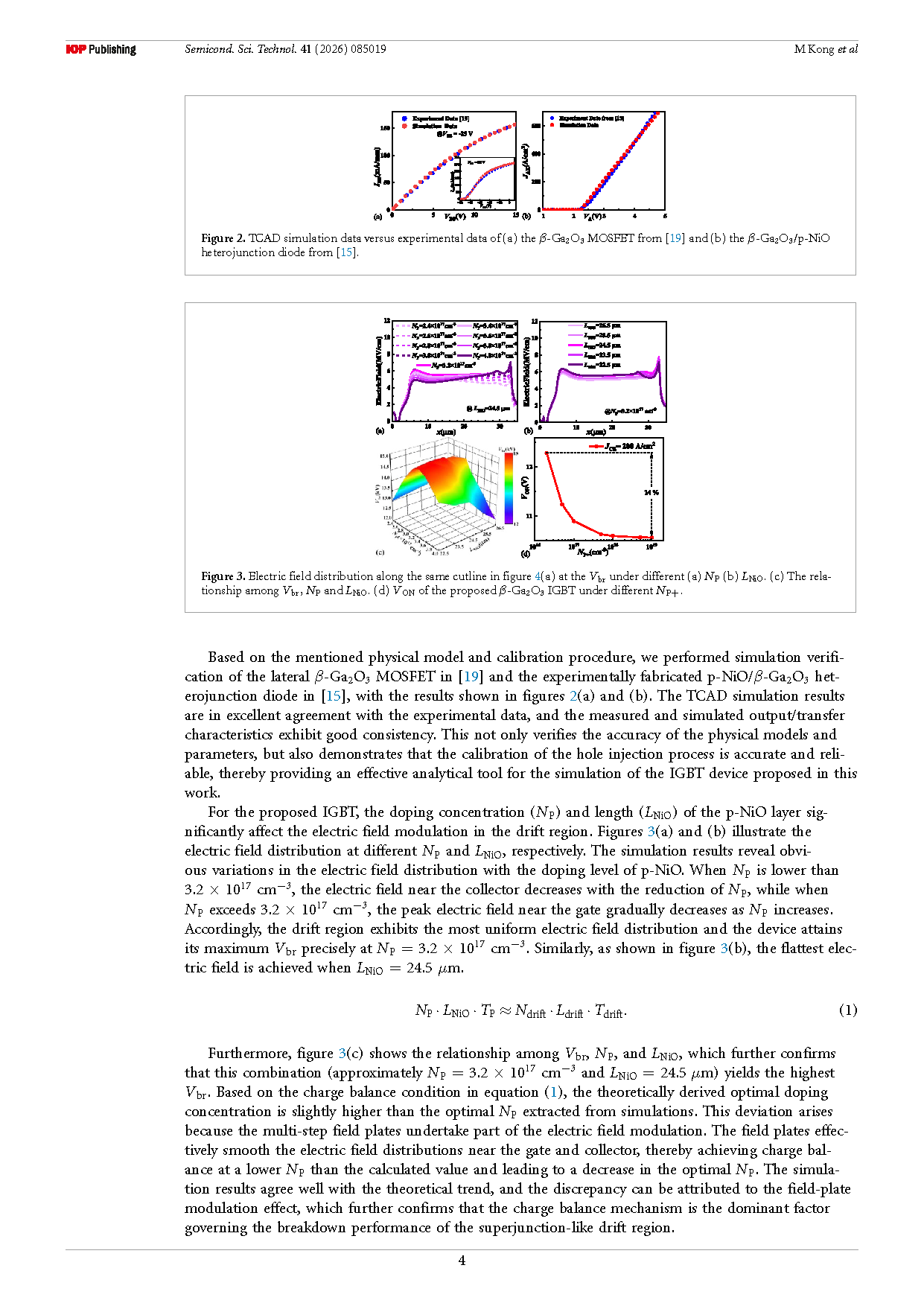
Figure 2. TCAD simulation data versus experimental data of (a) the β-Ga₂O₃ MOSFET from [19] and (b) the β-Ga₂O₃/p-NiO heterojunction diode from [15].
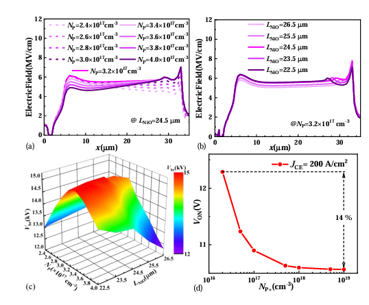
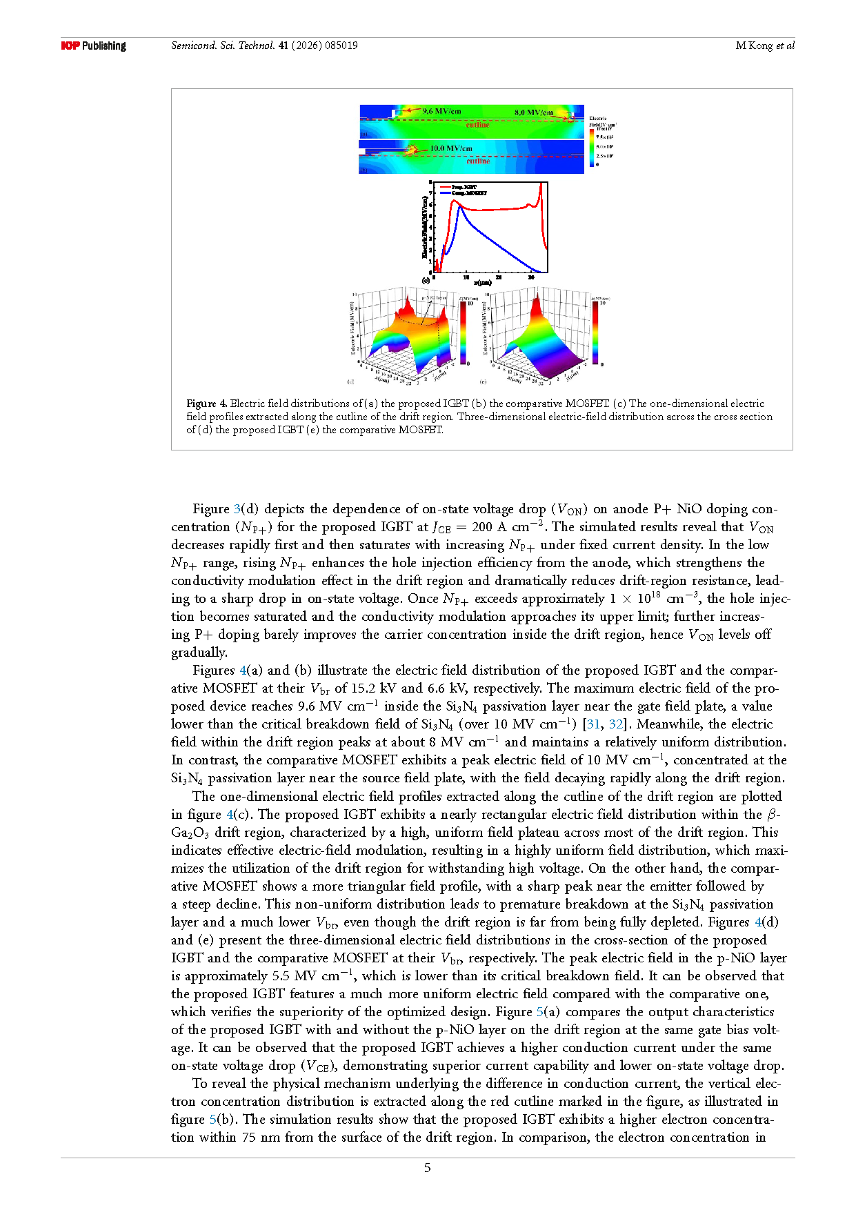
Figure 3. Electric field distribution along the same cutline in Fig. 4 (a) at the Vbr under different (a) NP (b) LNiO. (c) The relationship among Vbr, NP and LNiO. (d) VON of the proposed β-Ga₂O₃ IGBT under different NP+.
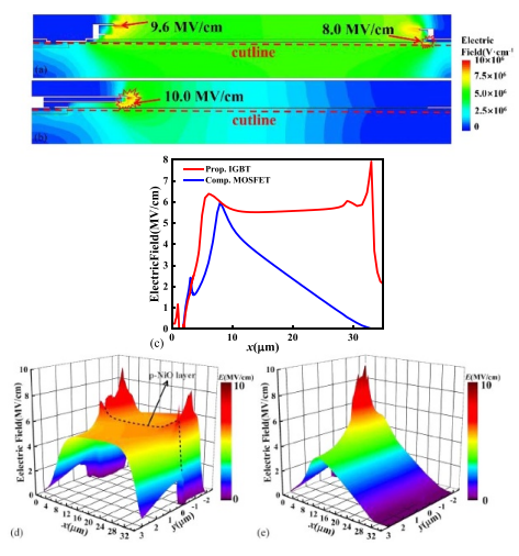
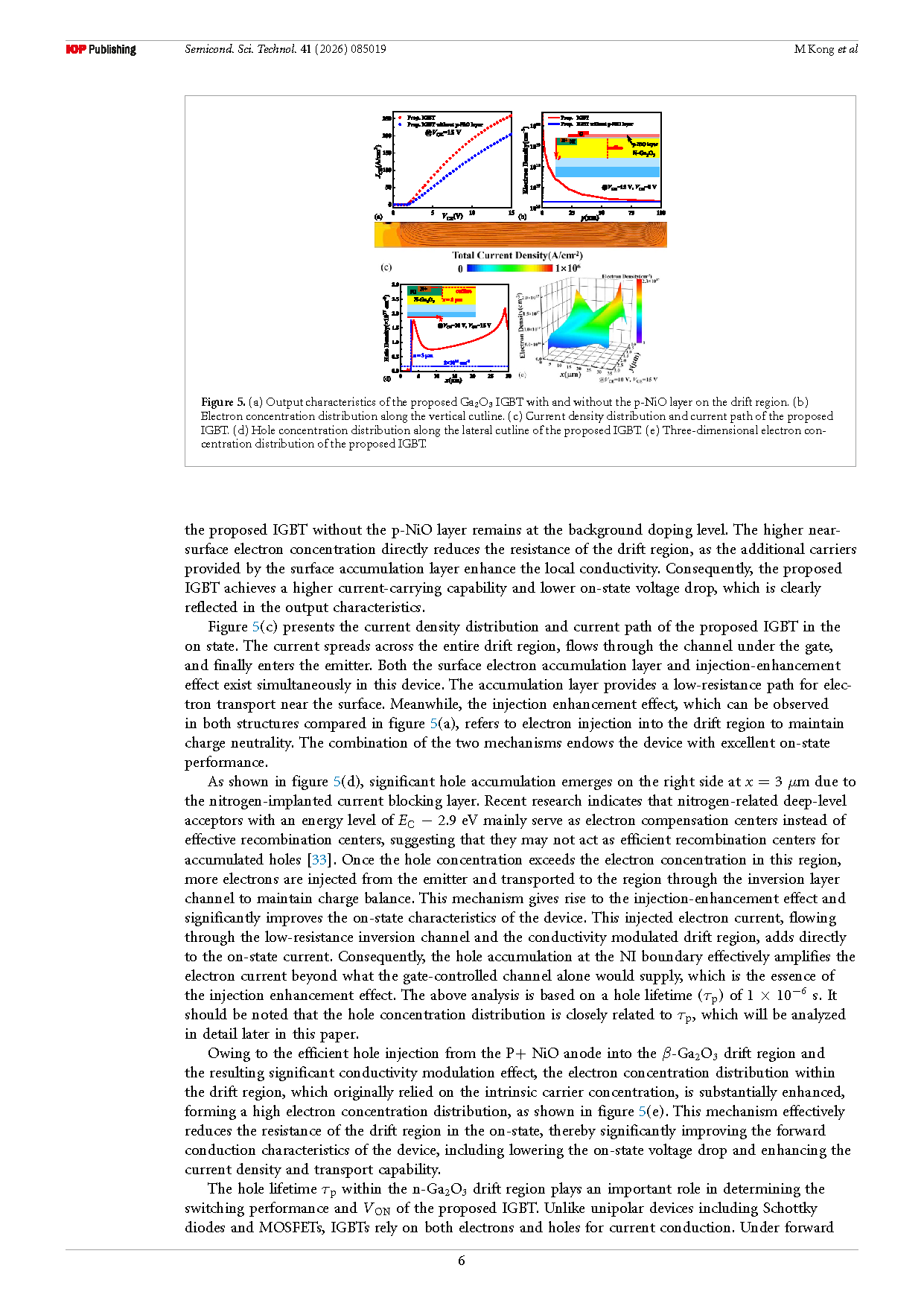
Figure 4. Electric field distributions of (a) the proposed IGBT (b) the comparative MOSFET. (c) The one-dimensional electric field profiles extracted along the cutline of the drift region. Three-dimensional electric-field distribution across the cross section of (d) the proposed IGBT (e) the comparative MOSFET.
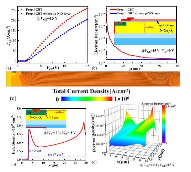
Figure 5. (a) Output characteristics of the proposed Ga₂O₃ IGBT with and without the p-NiO layer on the drift region. (b) Electron concentration distribution along the vertical cutline. (c) Current density distribution and current path of the proposed IGBT. (d) Hole concentration distribution along the lateral cutline of the proposed IGBT. (e) Three-dimensional electron concentration distribution of the proposed IGBT.
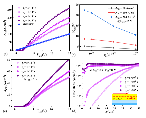
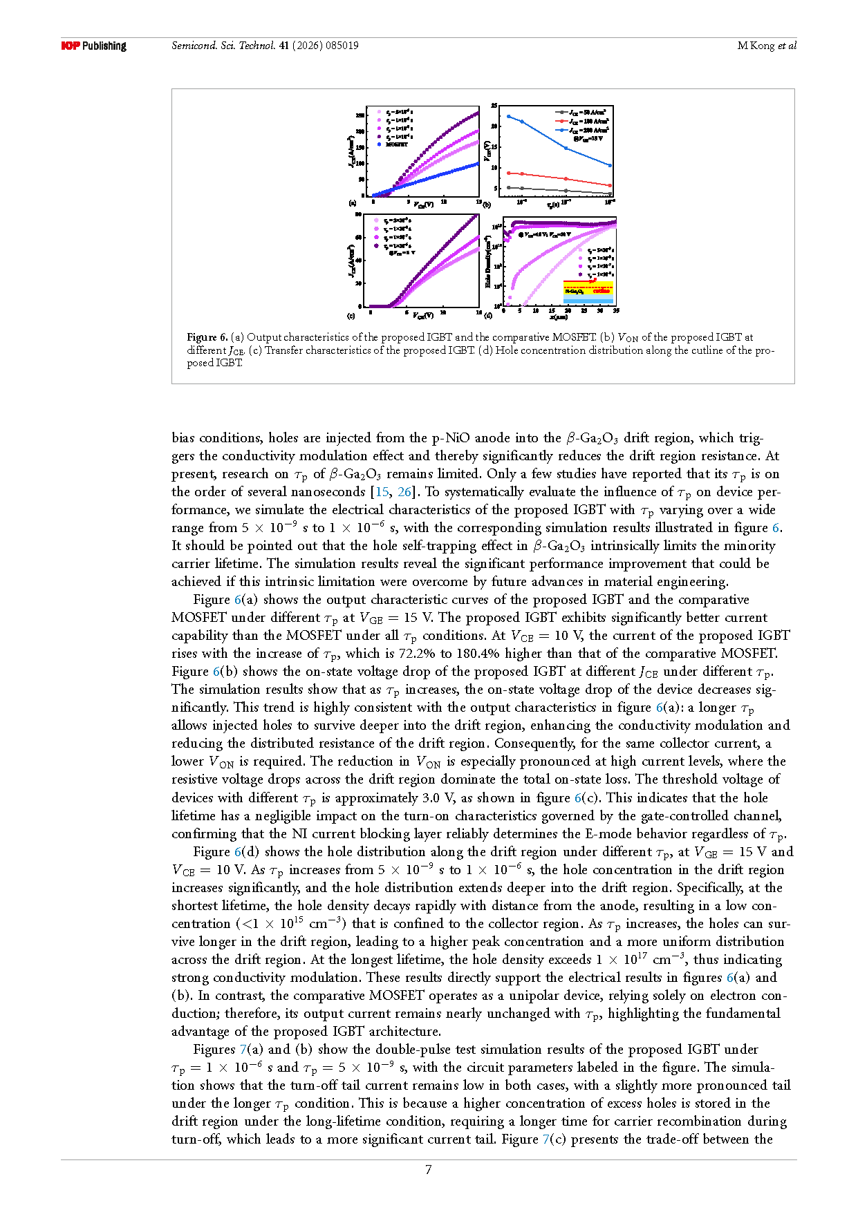
Figure 6. (a) Output characteristics of the proposed IGBT and the comparative MOSFET. (b) VON of the proposed IGBT at different JCE. (c) Transfer characteristics of the proposed IGBT. (d) Hole concentration distribution along the cutline of the proposed IGBT.
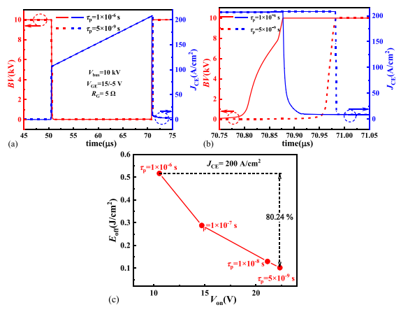
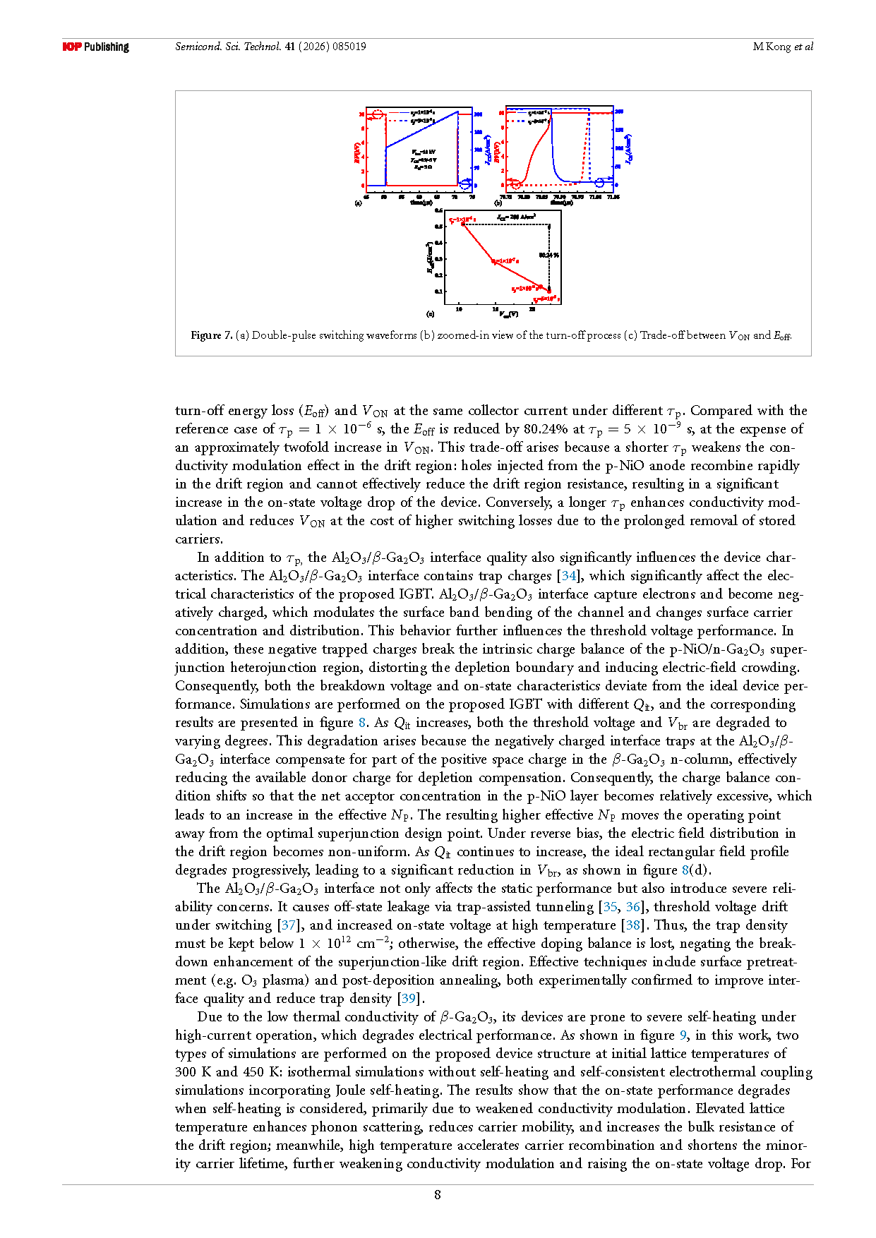
Figure 7. (a) Double-pulse switching waveforms (b) zoomed-in view of the turn-off process (c) Trade-off between VON and Eoff.
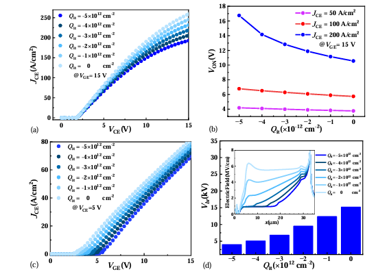
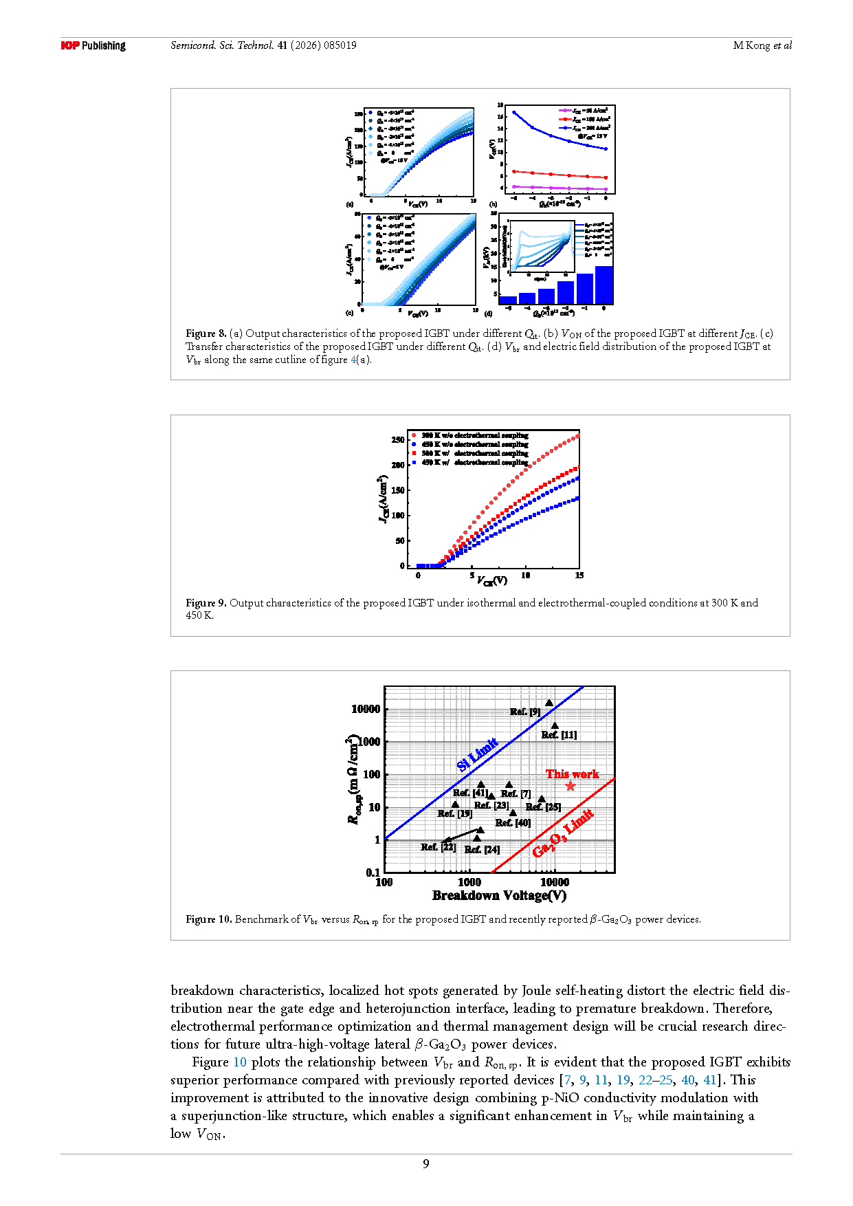
Figure 8. (a) Output characteristics of the proposed IGBT under different Qit (b) VON of the proposed IGBT at different JCE. (c) Transfer characteristics of the proposed IGBT under different Qit. (d) Vbr and electric field distribution of the proposed IGBT at Vbr along the same cutline of Fig. 4 (a).
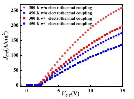
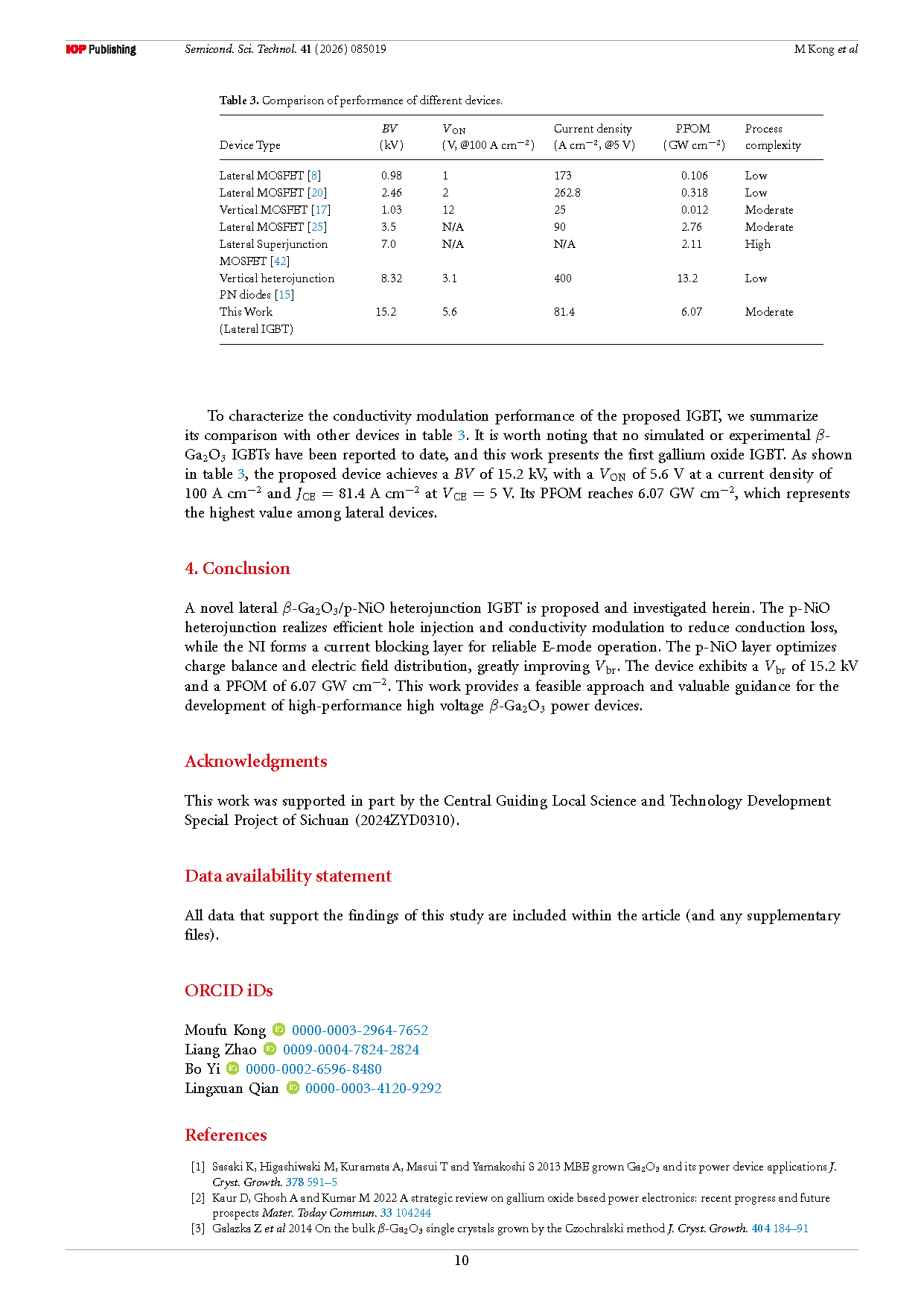
Figure 9. Output characteristics of the proposed IGBT under isothermal and electrothermal-coupled conditions at 300 K and 450 K.
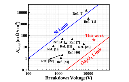
Figure 10. Benchmark of Vbr versus Ron,sp for the proposed IGBT and recently reported β-Ga₂O₃ power devices.
DOI :
10.1088/1361-6641/ae9c6b
Instruction
Official Account

Cooperation
Top
