


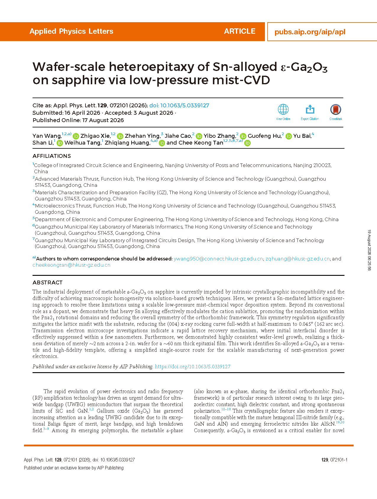
Researchers from Nanjing University of Posts and Telecommunications, The Hong Kong University of Science and Technology (Guangzhou) have published a dissertation titled "Wafer-scale heteroepitaxy of Sn-alloyed ε-Ga₂O₃ on sapphire via low-pressure mist-CVD" in Applied Physics Letters.
Background
Ultra-wide-bandgap ε-Ga₂O₃ features large piezoelectric coefficient, high dielectric constant and strong spontaneous polarization, and can realize heterogeneous integration with hexagonal III-nitrides, which makes it a promising candidate for next-generation power and radio-frequency devices. Nevertheless, ε-Ga₂O₃ is a metastable polymorph. When heteroepitaxially grown on sapphire substrates, crystallographic symmetry mismatch generates multiple sets of 120° rotational domains, and domain boundaries induce lattice distortion which severely degrades crystalline quality. Meanwhile, solution-based mist-CVD growth is affected by precursor mist flow and evaporation dynamics, making wafer-level uniformity of thickness and crystallinity difficult to achieve. High-performance films are only obtained in small localized regions. At present, feasible strategies that simultaneously tackle domain defects and large-area non-uniformity are lacking, which hinders the industrial deployment of ε-Ga₂O₃ and calls for epitaxy technologies with both high crystal quality and wafer-scale homogeneity.
Abstract
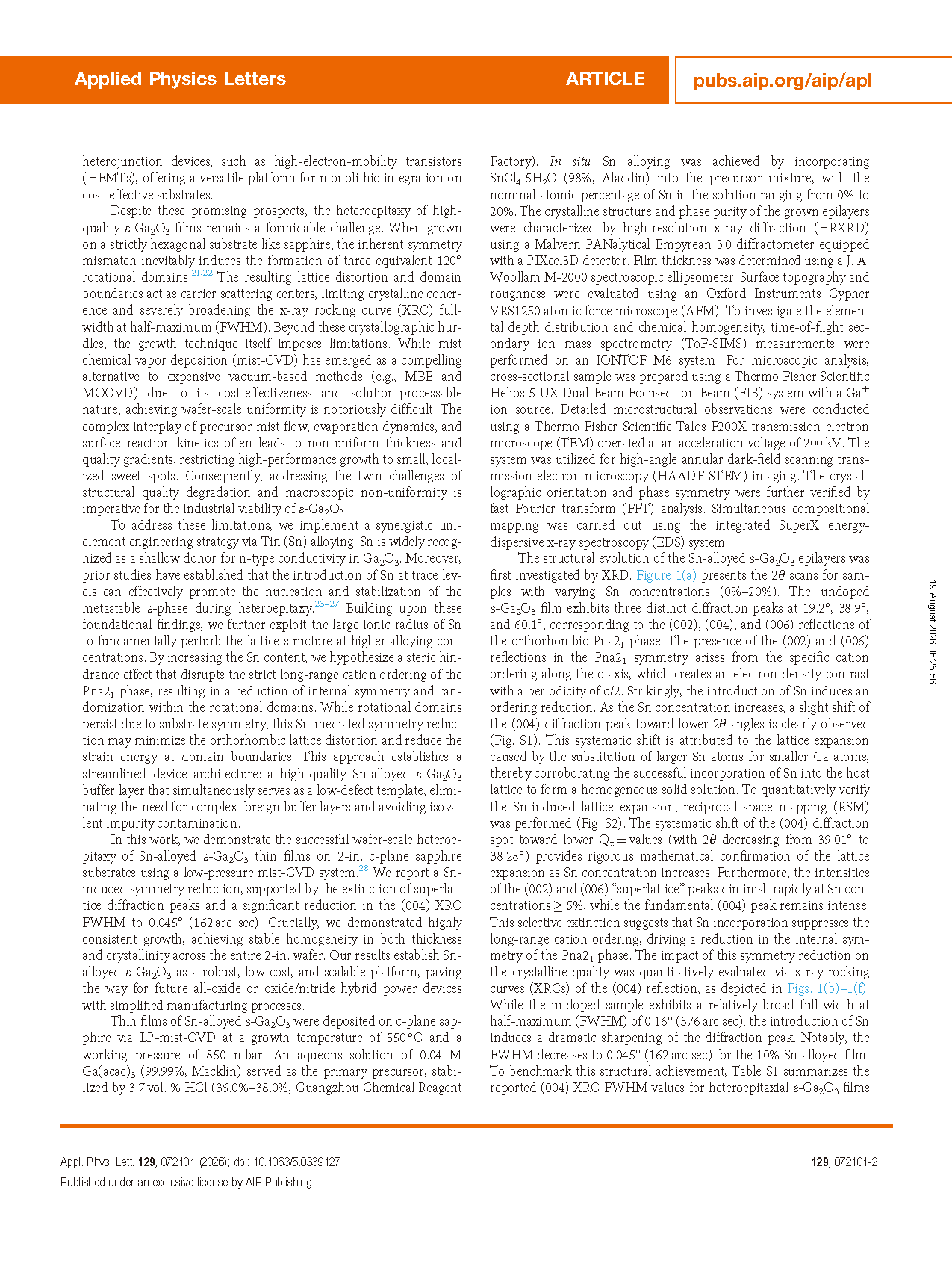
The industrial deployment of metastable ε-Ga₂O₃ on sapphire is currently impeded by intrinsic crystallographic incompatibility and the difficulty of achieving macroscopic homogeneity via solution-based growth techniques. Here, we present a Sn-mediated lattice engineering approach to resolve these limitations using a scalable low-pressure mist-chemical vapor deposition system. Beyond its conventional role as a dopant, we demonstrate that heavy Sn alloying effectively modulates the cation sublattice, promoting the randomization within the Pna2₁ rotational domains and reducing the overall symmetry of the orthorhombic framework. This symmetry regulation significantly mitigates the lattice misfit with the substrate, reducing the (004) x-ray rocking curve full-width at half-maximum to 0.045° (162 arc sec). Transmission electron microscope investigations indicate a rapid lattice recovery mechanism, where initial interfacial disorder is effectively suppressed within a few nanometers. Furthermore, we demonstrated highly consistent wafer-level growth, realizing a thickness deviation of merely ~2 nm across a 2-in. wafer for a ~60 nm thick epitaxial film. This work identifies Sn-alloyed ε-Ga₂O₃ as a versatile and high-fidelity template, offering a simplified single-source route for the scalable manufacturing of next-generation power electronics.
Highlights
Propose Sn-mediated lattice engineering strategy via low-pressure mist-CVD to modulate cation sublattice and reduce orthorhombic-phase symmetry of ε-Ga₂O₃.
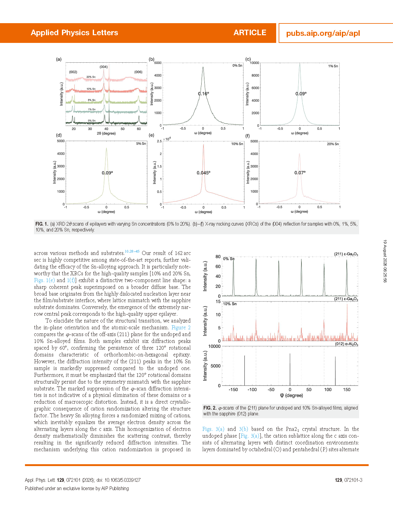
High Sn alloying randomizes cation arrangement inside rotational domains, greatly improves crystal quality with (004) XRC FWHM down to 0.045° (162 arc sec).
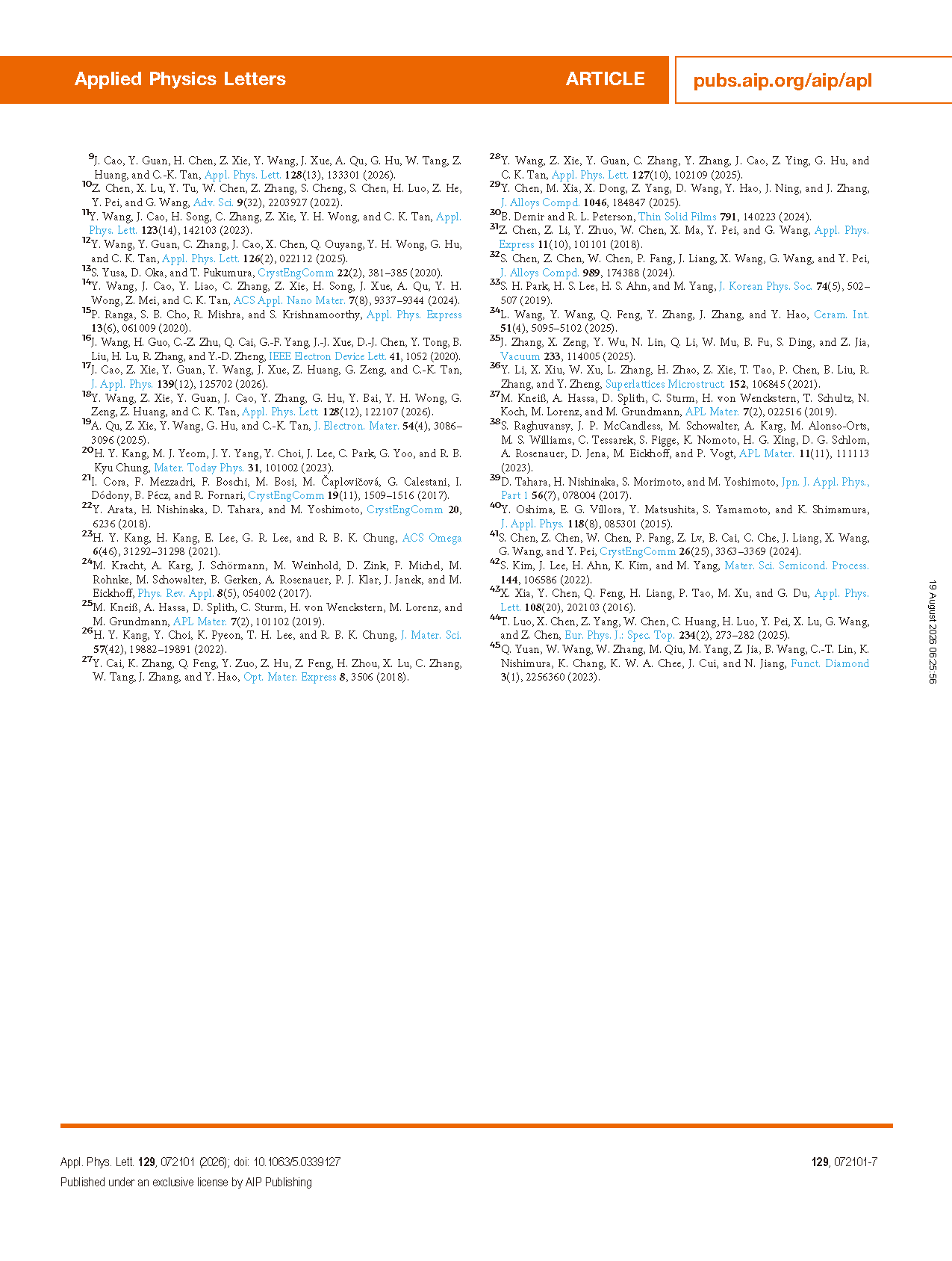
Reveal self-healing lattice recovery mechanism: interfacial disorder is suppressed within several nanometers above sapphire substrate.
Realize 2-inch wafer-scale ε-Ga₂O₃ epitaxy with only 2 nm thickness variation, providing high-quality template for power-device manufacturing.
Conclusion
In summary, we have successfully addressed the long-standing crystallographic and scalability bottlenecks in the heteroepitaxy of metastable ε-Ga₂O₃ on sapphire. By implementing a uni-element Sn-alloying strategy via a scalable low-pressure mist-CVD system, we realized high-quality, wafer-scale epilayers on 2-in. substrates. Our investigation reveals that high-concentration Sn incorporation perturbs the cation ordering of the orthorhombic Pna2₁ phase, inducing a reduction in structural symmetry and driving randomization within the rotational domains, resulting in a record-low (004) XRC FWHM of 0.045° (162 arc sec). Microscopic analyses further revealed a self-healing growth mechanism, where the initial interfacial disorder is largely suppressed within a thin transition layer (~5 nm), evolving into a high-quality epitaxial layer. Crucially, we demonstrated that this high crystalline quality is maintained uniformly across the entire 2-in. wafer. The ~60 nm buffer layer exhibits stable macroscopic homogeneity, with a thickness variation of only ~2 nm across the full substrate. Consequently, this work establishes Sn-alloyed ε-Ga₂O₃ as a robust and low-cost buffer platform. By eliminating the need for complex foreign buffer layers, this strategy paves the way for the streamlined manufacturing of high-performance Ga₂O₃ power electronics.
Project Support
The work was supported by the C. K. Tan start-up fund from the Hong Kong University of Science and Technology (Guangzhou); the Guangzhou Municipal Science and Technology Project (Nos. 2023A03J0003, 2023A03J0013, 2023A04J0310, and 2023A03J0152); the Department of Education of Guangdong Province (No. 2024ZDZX1005); the State Administration of Foreign Experts Affairs (No. Y20240005); the Matching Funding for Selected Talent of National Programs (CZ118SC24007); the National Major Talent Project (CZ118SC25005); and the Excellent Young Scientists Fund (overseas) (RK118QN24006). This work was supported by the Materials Characterization and Preparation Facility (MCPF) and the Green Materials Laboratory at the Hong Kong University of Science and Technology (Guangzhou).
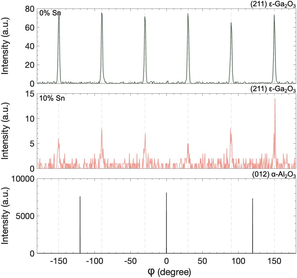
FIG. 1. (a) XRD 2θ scans of epilayers with varying Sn concentrations (0% to 20%). (b)–(f) X-ray rocking curves (XRCs) of the (004) reflection for samples with 0%, 1%, 5%, 10%, and 20% Sn, respectively.
FIG. 2. φ-scans of the (211) plane for undoped and 10% Sn-alloyed films, aligned with the sapphire (012) plane.
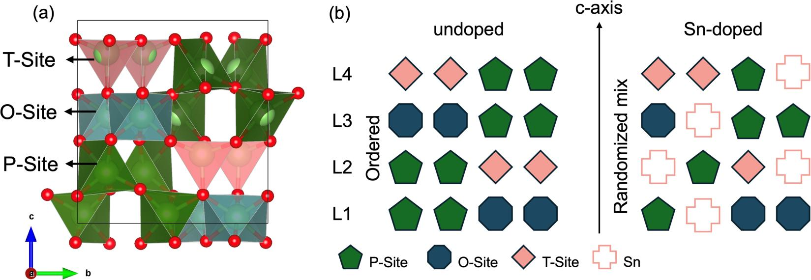
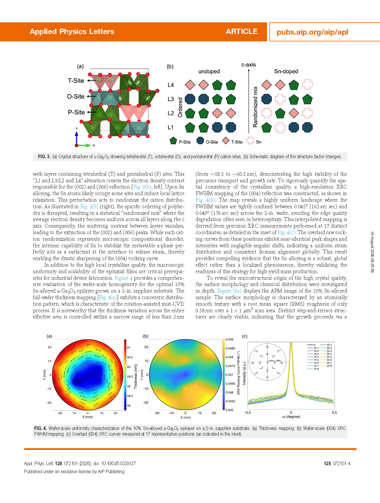
FIG. 3. (a) Crystal structure of ε-Ga₂O₃ showing tetrahedral (T), octahedral (O), and pentahedral (P) cation sites. (b) Schematic diagram of the structure factor changes.
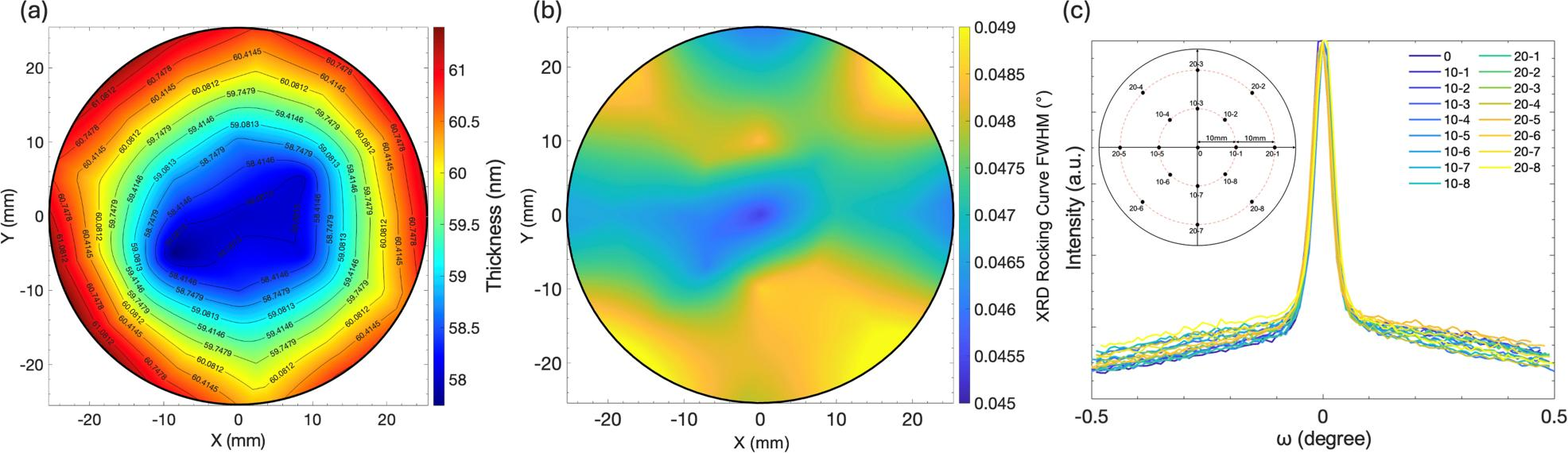
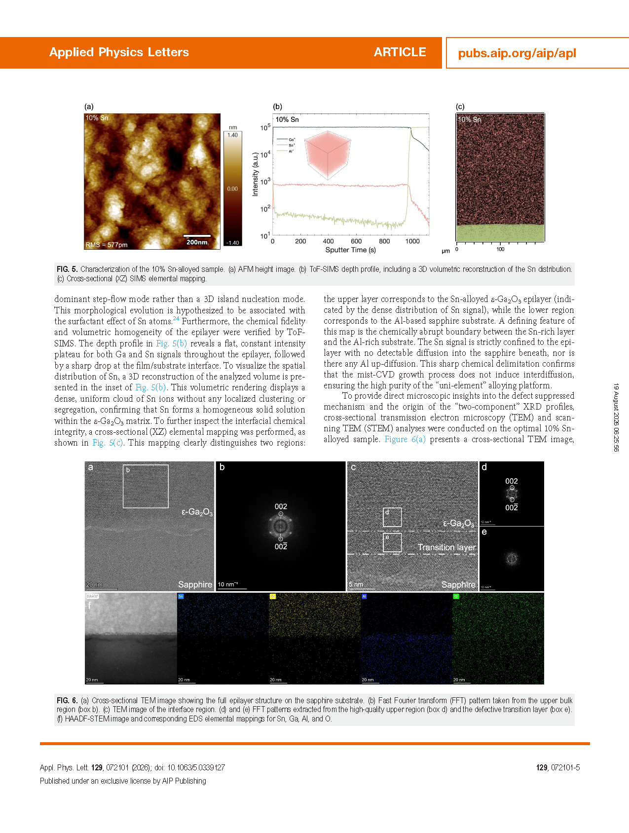
FIG. 4. Wafer-scale uniformity characterization of the 10% Sn-alloyed ε-Ga₂O₃ epilayer on a 2-in. sapphire substrate. (a) Thickness mapping. (b) Wafer-scale (004) XRC FWHM mapping. (c) Overlaid (004) XRC curves measured at 17 representative positions (as indicated in the inset).
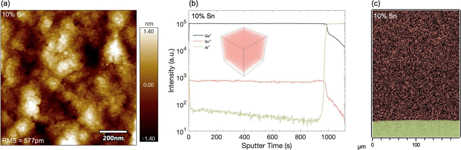
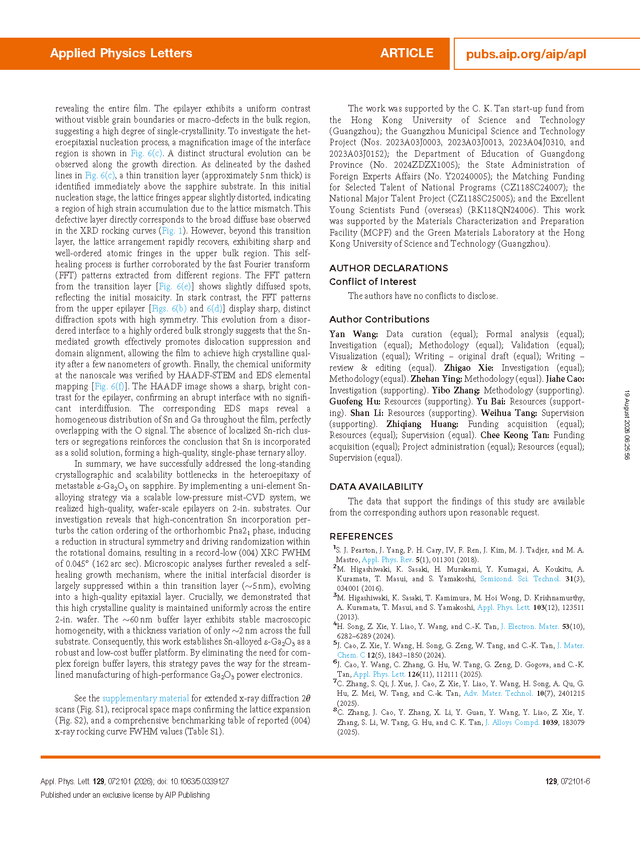
FIG. 5. Characterization of the 10% Sn-alloyed sample. (a) AFM height image. (b) ToF-SIMS depth profile, including a 3D volumetric reconstruction of the Sn distribution. (c) Cross-sectional (XZ) SIMS elemental mapping.
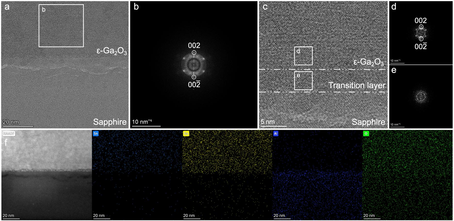
FIG. 6. (a) Cross-sectional TEM image showing the full epilayer structure on the sapphire substrate. (b) Fast Fourier transform (FFT) pattern taken from the upper bulk region (box b). (c) TEM image of the interface region. (d) and (e) FFT patterns extracted from the high-quality upper region (box d) and the defective transition layer (box e). (f) HAADF-STEM image and corresponding EDS elemental mappings for Sn, Ga, Al, and O.
DOI:
doi.org/10.1063/5.0339127
Instruction
Official Account

Cooperation
Top
