


Researchers from The Ohio State University have published a dissertation titled "MOCVD Growth of (011) β-Ga₂O₃ Films: Defect Control and Device Implication" in Crystal Growth & Design.
Background
β-Ga₂O₃ has emerged as a leading ultra-wide-bandgap semiconductor for next-generation power electronics due to its large bandgap (∼4.8 eV), controllable n-type doping, and high predicted breakdown field (~ 8 MV/cm). A key advantage over GaN, SiC, AlN, and diamond is the availability of high-quality native substrates produced by scalable, low-cost melt-growth methods, enabling large-area wafers with low defect densities and precise doping control. Driven by rising global energy demand, power electronics continue to require higher efficiency and reduced device footprint, motivating materials with higher breakdown strength than conventional WBG semiconductors. While vertical β-Ga₂O₃ devices—including Schottky diodes, p−n heterojunctions, and MOSFET-based structures—have shown strong performance progress, device metrics remain limited by challenges in growing thick, smooth, high-quality drift layers and by the absence of mature p-type doping.
High-breakdown-voltage power devices require thick drift layers with smooth surfaces and precisely controlled low doping, motivating high growth rates without compromising epitaxial quality. Thick β-Ga₂O₃ films have been mostly grown by halide vapor-phase epitaxy (HVPE) and MOCVD on β-Ga₂O₃ substrates of various orientations. HVPE can rapidly deposit thick (001) β-Ga₂O₃ layers (>5 μm/h) and currently supplies most drift layers used in vertical devices. However, HVPE films typically exhibit step- and pit-induced roughness that necessitates chemical mechanical polishing (CMP) prior to fabrication, increasing cost, risking surface contamination, and complicating the in-situ growth of multilayer structures such as p-n junctions. In contrast, MOCVD offers smoother uniform as-grown surfaces and precise control over thickness, doping, and alloy composition, enabling monolithic multilayer device structure growth. Additionally, HVPE growth rates vary significantly with β-Ga₂O₃ substrate crystallographic orientation, whereas MOCVD typically yields similar growth rates across different orientations.
Recently, (011) β-Ga₂O₃ homoepitaxy has shown strong potential for high quality growth, including the demonstration of 10 kV devices. In the team’s previous work, high-quality (011) β-Ga₂O₃ drift layers up to 20 μm thick were achieved with very low AFM roughness and narrow XRD rocking-curve FWHM, although dent or pit-type defects remained a challenge. Prior HCl-based HVPE studies also reported pit densities of ~ 3.7 × 10³ cm⁻² for ∼3.6 μm-thick films, underscoring the persistent difficulty of defect suppression. Because minimizing defect density is essential for high-yield, high-performance vertical devices, this study systematically studies substrate pre-treatment and growth conditions to suppress defect formation and evaluates their device-level impact through vertical Schottky barrier diode (SBD) fabrication.
Abstract
β-Ga₂O₃ is a promising ultrawide‑bandgap semiconductor for high‑power electronics; however, the realization of thick, low‑defect drift layers at high growth rates remains challenging. In this work, metalorganic chemical vapor deposition (MOCVD) growth of (011) β-Ga₂O₃ drift layers on (011) β-Ga₂O₃ substrates is optimized using a far‑injection showerhead reactor with trimethylgallium (TMGa) and O₂ precursors. The effects of chemical pre‑treatment, in situ oxygen annealing, wafer carrier rotation, and pulse‑flow (PF) β-Ga₂O₃ interlayers are systematically investigated to correlate growth conditions with defect density. Chemical treatment B [18% HCl (10 min) + deionized (DI) water (10 min) + 49% HF (30 min)], combined with 1 h of in situ annealing at 900 °C, minimizes defect density under the selected growth conditions. On the basis of this pre‑treatment and annealing process, incorporation of a single PF1 interlayer (∼30 nm thick) further suppresses defect formation. The complete set of processes can reduce the defect density by more than one order of magnitude, while inserting only the PF1 interlayer alone achieves roughly a 3.5‑fold defect reduction. Atomic force microscopy (AFM) reveals sub‑nanometer root mean square (RMS) roughness and step‑flow morphology for ∼11 μm thick films. High‑resolution X‑ray diffraction (XRD) rocking curves confirm the preserved crystalline quality. Field‑plated Schottky barrier diodes (SBDs) fabricated on optimized films exhibit excellent forward conduction, low reverse leakage, and improved breakdown performance, highlighting the importance of defect control for high‑performance vertical power devices.
Highlights
The team systematically compared three chemical treatment methods and found that Treatment B (18% HCl for 10 min + deionized water for 10 min + 49% HF for 30 min), combined with 1 h of in situ oxygen annealing at 900 °C, produced the smoothest films with the lowest defect density.
The team investigated the influences of position, thickness and pulse timing of pulse‑flow interlayers. It is found that under the optimal substrate chemical pre‑treatment and in‑situ annealing conditions, inserting a single ~ 30 nm PF1 pulse‑flow interlayer in the middle of drift layer can effectively block vertical defect propagation. The full process achieves defect density reduction by more than one order of magnitude, while the PF1 interlayer alone only provides approximately 3.5‑fold defect suppression.
High-quality thick epilayers maintained under high-speed growth: ~11 μm-thick (011) β-Ga₂O₃ homoepitaxial films were obtained with a maximum growth rate of 5.5 μm/h. The epilayers maintain sub-nanometer surface roughness and step-flow growth mode. XRD rocking-curve FWHM values are even smaller than those of the starting substrate, demonstrating excellent crystalline quality.
Field‑plated vertical Schottky barrier diodes were fabricated. Devices from defect‑free regions show near‑unity ideality factor and 640‑740 V breakdown voltage. Devices containing defects exhibit drastically elevated leakage and degraded breakdown voltage, directly proving the critical importance of defect control for β-Ga₂O₃ power devices.
Conclusion
In summary, this study provides a promising pathway for reducing defect formation during the fast MOCVD growth of thick (011) β-Ga₂O₃ films. Our results show that defect formation can be suppressed through specific surface preparation and growth‑mode engineering. Among the studied pre‑growth treatments, HCl‑ and HF‑based chemical treatment, followed by a 1 h in situ oxygen annealing at 900 °C, consistently produced the smoothest films with the lowest defect densities, whereas extending annealing time or increasing annealing temperature degraded the material quality. Another outcome of this work is the implementation of a pulse‑flow strategy: on the premise of optimal pre‑treatment and annealing, inserting a single PF1 β‑Ga₂O₃ interlayer at the middle of the drift layer yields an effective defect reduction.High‑resolution XRD rocking curves confirm the high crystalline quality of the as‑grown film, and AFM shows that step‑flow morphology and sub‑nanometer roughness are maintained for ∼11 μm films grown at high growth rates. Finally, preliminary SBD device fabrication and characterization indicate the critical need for defect control: SBDs fabricated on defect‑free regions show stable electrical behavior, while defected areas exhibit elevated leakage and reduced breakdown. These results provide guidance for the future development of (011) β-Ga₂O₃ for high‑power electronics.
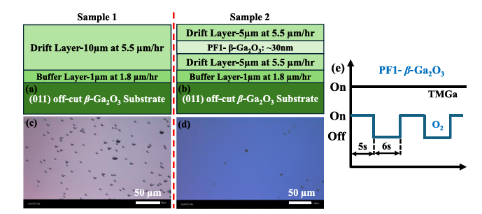
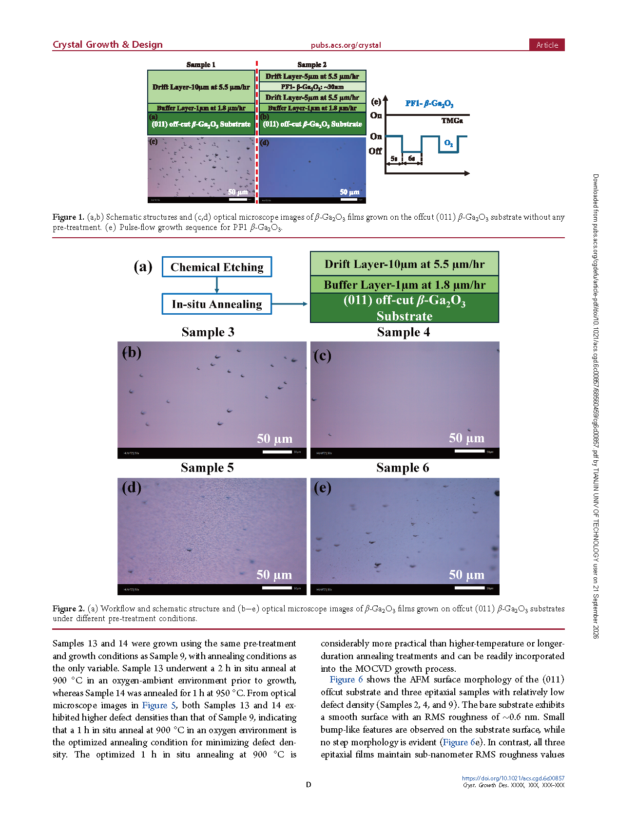
Fig 1. (a,b) Schematic structures and (c,d) optical microscope images of β-Ga₂O₃ films grown on the offcut (011) β-Ga₂O₃ substrate without any pre-treatment. (e) Pulse-flow growth sequence for PF1 β-Ga₂O₃.
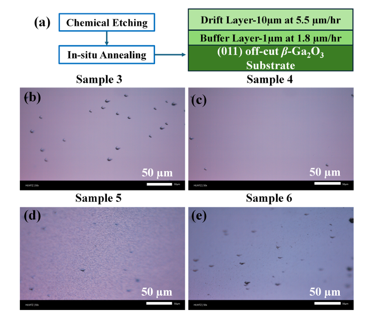
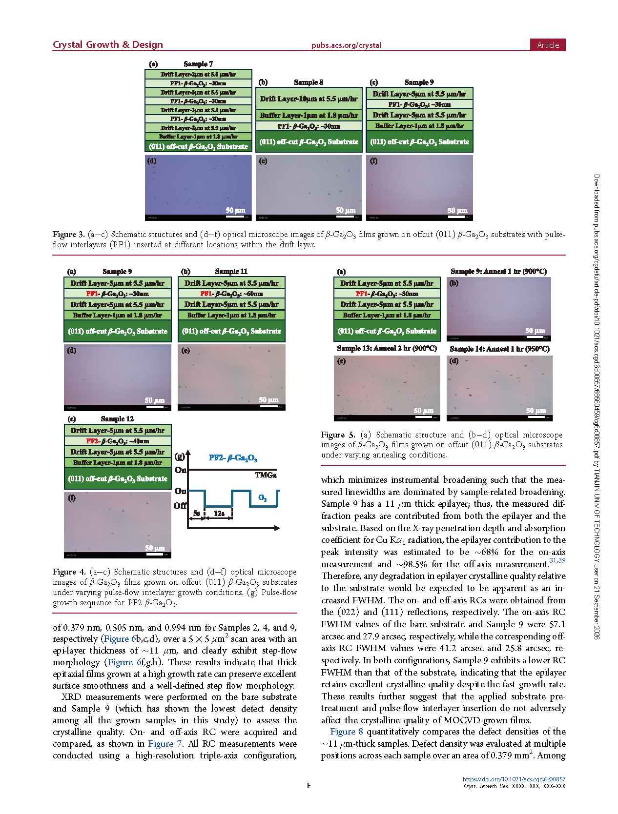
Fig 2. (a) Workflow and schematic structure and (b−e) optical microscope images of β-Ga₂O₃ films grown on offcut (011) β-Ga₂O₃ substrates under different pre-treatment conditions.
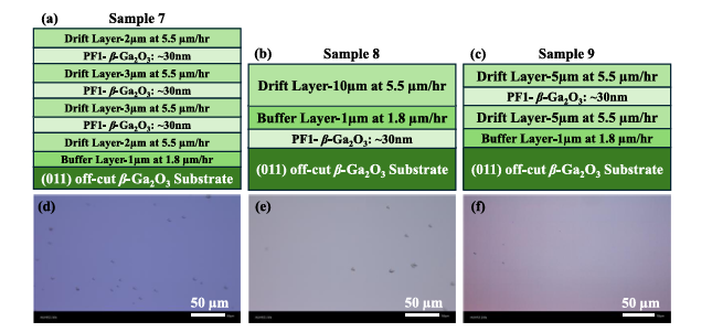
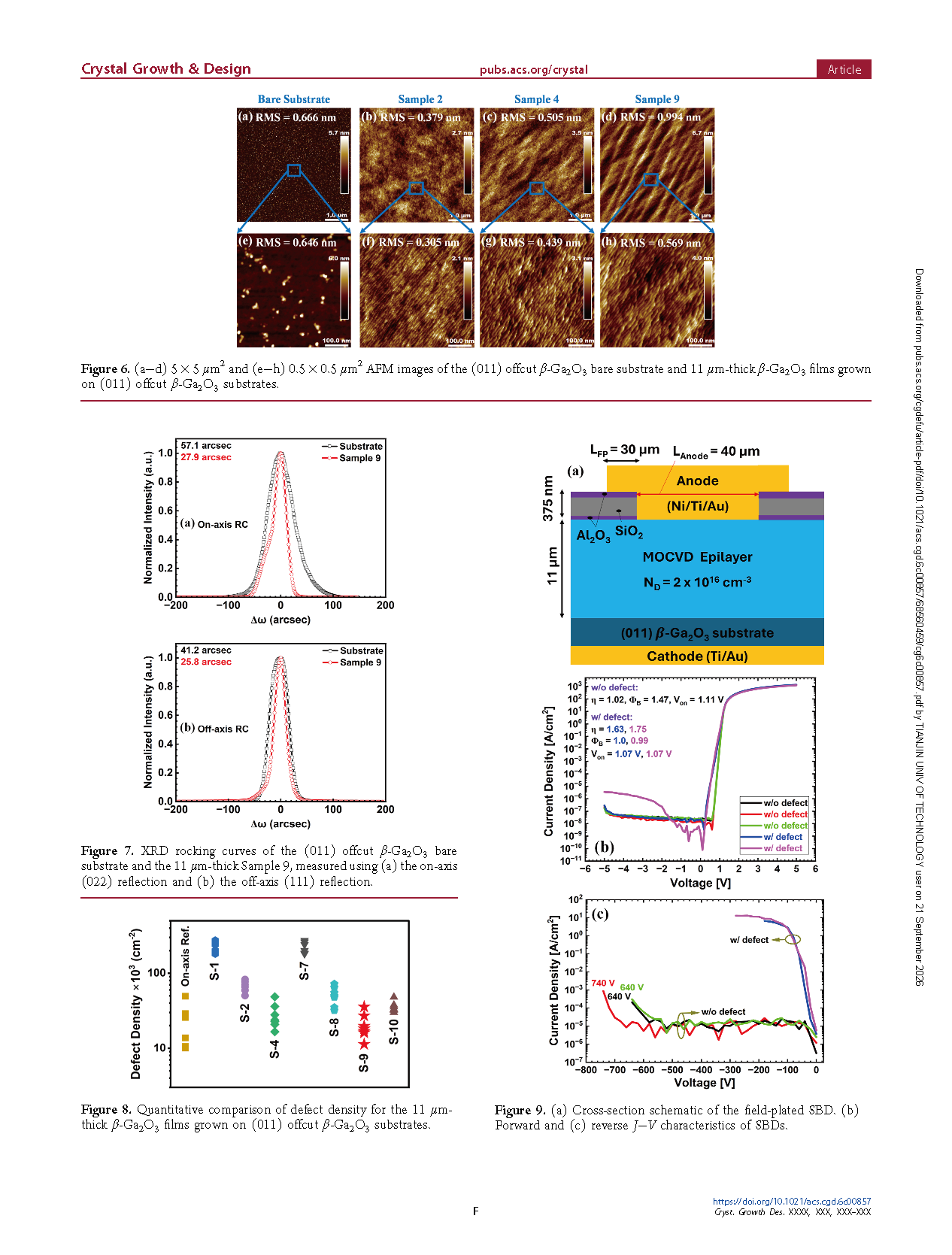
Fig 3. (a−c) Schematic structures and (d−f) optical microscope images of β-Ga₂O₃ films grown on offcut (011) β-Ga₂O₃ substrates with pulse-flow interlayers (PF1) inserted at different locations within the drift layer.
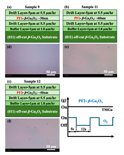
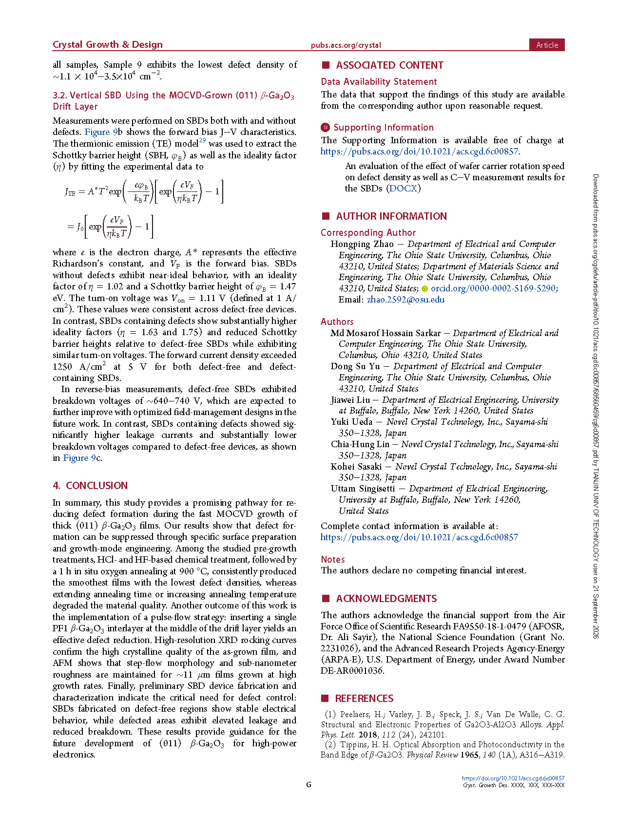
Fig 4. (a−c) Schematic structures and (d−f) optical microscope images of β-Ga₂O₃ films grown on offcut (011) β-Ga₂O₃ substrates under varying pulse-flow interlayer growth conditions. (g) Pulse-flow growth sequence for PF2 β-Ga₂O₃.
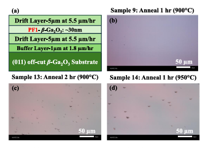
Fig 5. (a) Schematic structure and (b−d) optical microscope images of β-Ga₂O₃ films grown on offcut (011) β-Ga₂O₃ substrates under varying annealing conditions.
DOI:
doi.org/10.1021/acs.cgd.6c00857
Instruction
Official Account

Cooperation
Top
