


Researchers from the“State Key Laboratory of Crystal Materials, Institute of Novel Semiconductors, Institute of Crystal Materials, Shandong University, and Shenzhen Research Institute of Shandong University” have published a dissertation titled "Complementary Material Integration: Co-Optimizing Low Noise and High Signal in X-Ray Detectors for High Detectivity via β-Ga₂O₃/3D/2D Metal Halide Perovskite Heterojunction" in Advanced Functional Materials.
Background
X‑rays have been widely used in medical imaging, security inspection, and industrial flaw detection. Given the hazards of ionizing radiation, adherence to the as low as reasonably achievable (ALARA) principle is imperative. To achieve high‑contrast imaging under low‑dose conditions, detectors must exhibit both high sensitivity and low detection limits. In x‑ray detectors, sensitivity mainly depends on the electron‑hole pair creation energy, carrier mobility‑lifetime (µτ) product, x‑ray absorption efficiency, and photoconductive gain of the semiconductor material. The detection limit, on the other hand, is determined by the signal‑to‑noise ratio (SNR). High‑resistivity materials are essential to ensure low dark current, thereby minimizing noise. However, single semiconductor materials can hardly combine high resistivity, low electron‑hole pair creation energy and high µτ product. Silicon shows poor X‑ray absorption; amorphous selenium (a‑Se) possesses low µτ product. Although cadmium zinc telluride (CZT) delivers good performance, its commercialization is hindered by challenges in scalable crystal growth, compositional uniformity, and defect density control. As a fourth‑generation semiconductor, β-Ga₂O₃ features high density, tunable resistivity and good radiation hardness. Nevertheless, high‑resistivity doping degrades µτ product and reduces sensitivity. Metal halide perovskites (MHPs) have strong X‑ray absorption and large µτ product. Three‑dimensional (3D) MHPs provide high sensitivity yet suffer low resistivity and severe ion migration. Two‑dimensional (2D) MHPs obtain high resistivity at the cost of deteriorated carrier transport. Intrinsic performance trade‑offs exist in single‑material systems, calling for innovative strategies to break such bottlenecks.
Abstract
Achieving high-contrast imaging under low-dose x-rays is a core challenge for x-ray detectors, as co-optimizing low dark current and high sensitivity in a single material remains difficult. Herein, we propose a complementary material integration (CMI) strategy by combining a high resistivity wide bandgap oxide with a high µτ product perovskite. This strategy is demonstrated in the x-ray detector based on a β-Ga₂O₃/3D/2D metal halide perovskite (MHP) heterostructure. The high resistivity of β-Ga₂O₃ ensures low noise, while its combination with a 2D MHP layer effectively passivates the 3D MHP active layer, yielding both high performance and enhanced stability. The detector exhibits a large µτ product of 1.61 × 10⁻³ cm² V⁻¹, a dark current of only 1.09 pA at 100 V, and a high sensitivity of 7140 µC Gyair ⁻¹ cm⁻². These properties yield a high quasi-detectivity (S√A/IDark) of 354.86 C Gy⁻¹ cm⁻¹ A⁻¹/² and a low detection limit of 8.16 nGy s⁻¹. Furthermore, the detector realizes high-contrast imaging (SNR = 138.0) for x-rays at the medically safe dose (2.944 µGy s⁻¹). This study successfully realizes the co-optimization of low dark current, high sensitivity, and low detection limit, and provides a CMI strategy for high-performance x-ray imaging devices.
Highlights
The research team puts forward the complementary material integration (CMI) strategy. Instead of using one single semiconductor to fulfill all performance requirements, this strategy distributes functions between high‑resistivity oxide for low‑noise and perovskite with high mobility‑lifetime (µτ) product for high signal, overcoming the intrinsic trade‑off between resistivity and carrier transport.
β-Ga₂O₃/3D MAPbBr₃/2D MA₃Bi₂I₆Br₃ heterojunction devices are constructed. β-Ga₂O₃ acts as high-resistivity X-ray absorber. The 2D perovskite passivates defects and suppresses ion migration of 3D perovskite, and restrains dark current via band offset. The 3D perovskite guarantees efficient carrier transport.
At 100 V bias, the device delivers ultralow dark current of 1.09 pA, high sensitivity of 7140 µC Gyair⁻¹ cm⁻², ultra-low detection limit of 8.16 nGy s⁻¹, and superior quasi-detectivity compared with most reported oxide- and perovskite-based X-ray detectors. Dark-current drift is also greatly mitigated.
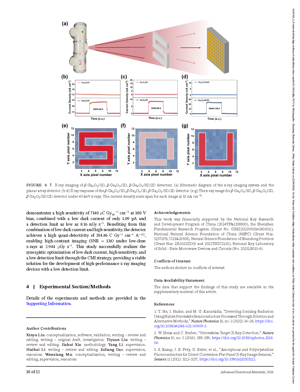
High-quality imaging with SNR = 138.0 is achieved at medically safe dose rate (2.944 µGy s⁻¹). The heterojunction detector also exhibits self-powered detection capability and decent ambient storage stability, showing promising prospects for clinical low-dose X-ray imaging.
Conclusion
In this work, we propose a CMI strategy that combines a high resistivity wide bandgap oxide with a high µτ product perovskite. We demonstrate this strategy by fabricating an x‑ray detector based on a β-Ga₂O₃/3D/2D MHP heterojunction, which exhibits an outstanding µτ product of 1.61 ×10⁻³ cm² V⁻¹ and a low dark current drift of 3.57 ×10⁻⁷ nA cm⁻¹ s⁻¹ V⁻¹. The detector demonstrates a high sensitivity of 7140 µC Gyair⁻¹ cm⁻² at 100 V bias, combined with a low dark current of only 1.09 pA and a detection limit as low as 8.16 nGy s⁻¹. Benefiting from this combination of low dark current and high sensitivity, the detector achieves a high quasi‑detectivity of 354.86 C Gy⁻¹ cm⁻¹ A⁻¹ᐟ², enabling high‑contrast imaging (SNR=138) under low‑dose x‑rays at 2.944 µGy s⁻¹. This study successfully realizes the synergistic optimization of low dark current, high sensitivity, and a low detection limit through the CMI strategy, providing a viable solution for the development of high‑performance x‑ray imaging devices with a low detection limit.
Project Support
This work was financially supported by the National Key Research and Development Program of China (2024YFA1208800), the Shenzhen Fundamental Research Program (Grant No. GJHZ20220913142605011), National Natural Science Foundation of China (NSFC) (Grant Nos. 52572176, U23A20358), Natural Science Foundation of Shandong Province (Grant Nos. ZR2023ZD05 and 2022TSGC2120), and National Key Laboratory of Solid-State Microwave Devices and Circuits (No. 2025LB015-4).
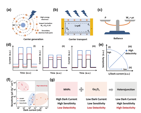
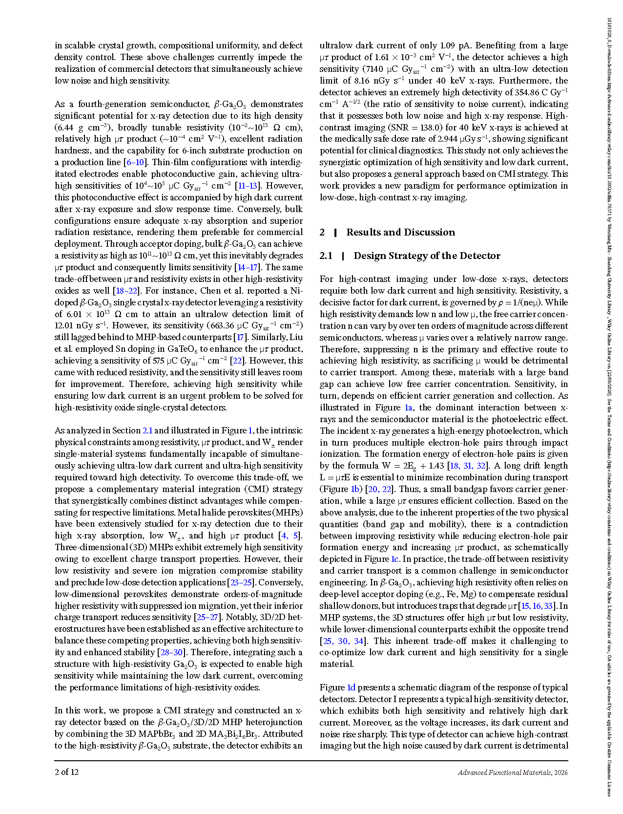
FIGURE 1. Design ideas of β-Ga₂O₃/MHPs x-ray detectors. Schematic diagram of the generation and separation (a), and transport (b) carriers in semiconductors under x-ray irradiation. (c) The trade-off relationship between resistivity, carrier formation energy, and µτ. (d) Schematic diagram of the typical relationship between dark current and photocurrent in x-ray detectors. (e) The trade-off relationship between dark current and sensitivity, (f) The relationship between dark current and sensitivity in typical metal halide perovskite and oxide (such as Ga₂O₃) x-ray detectors. (g) Design diagrams of x-ray detector adopted in this work and corresponding work mechanisms.
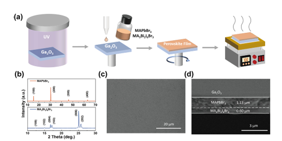
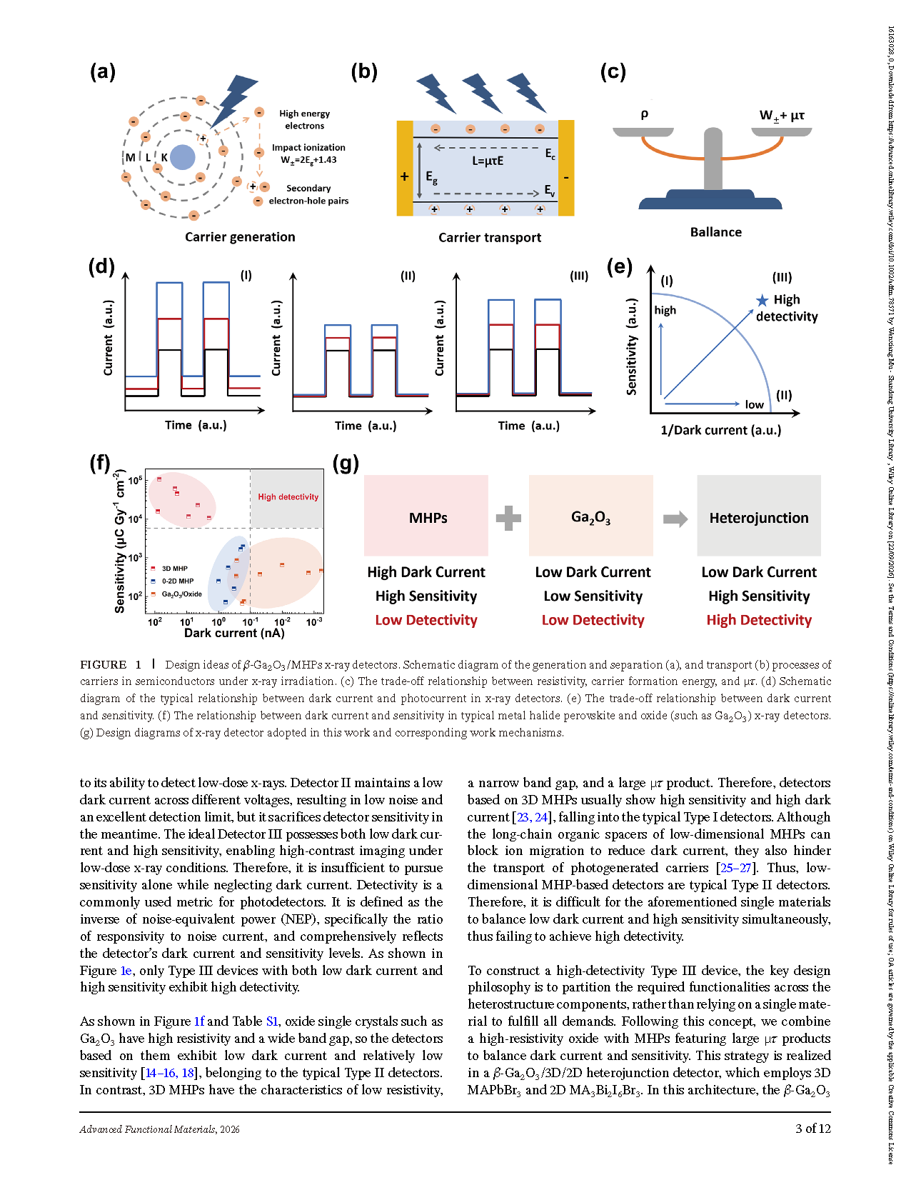
FIGURE 2. Fabrication and characterization of β-Ga₂O₃/MHP heterojunction. (a) The fabrication process of β-Ga₂O₃/MHP heterojunction. (b) XRD patterns for MAPbBr₃ and MA₃Bi₂I₆Br₃ films. (c) Surface and (d) cross-sectional SEM images of β-Ga₂O₃/MAPbBr₃/MA₃Bi₂I₆Br₃ film.
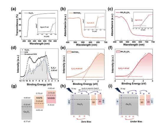
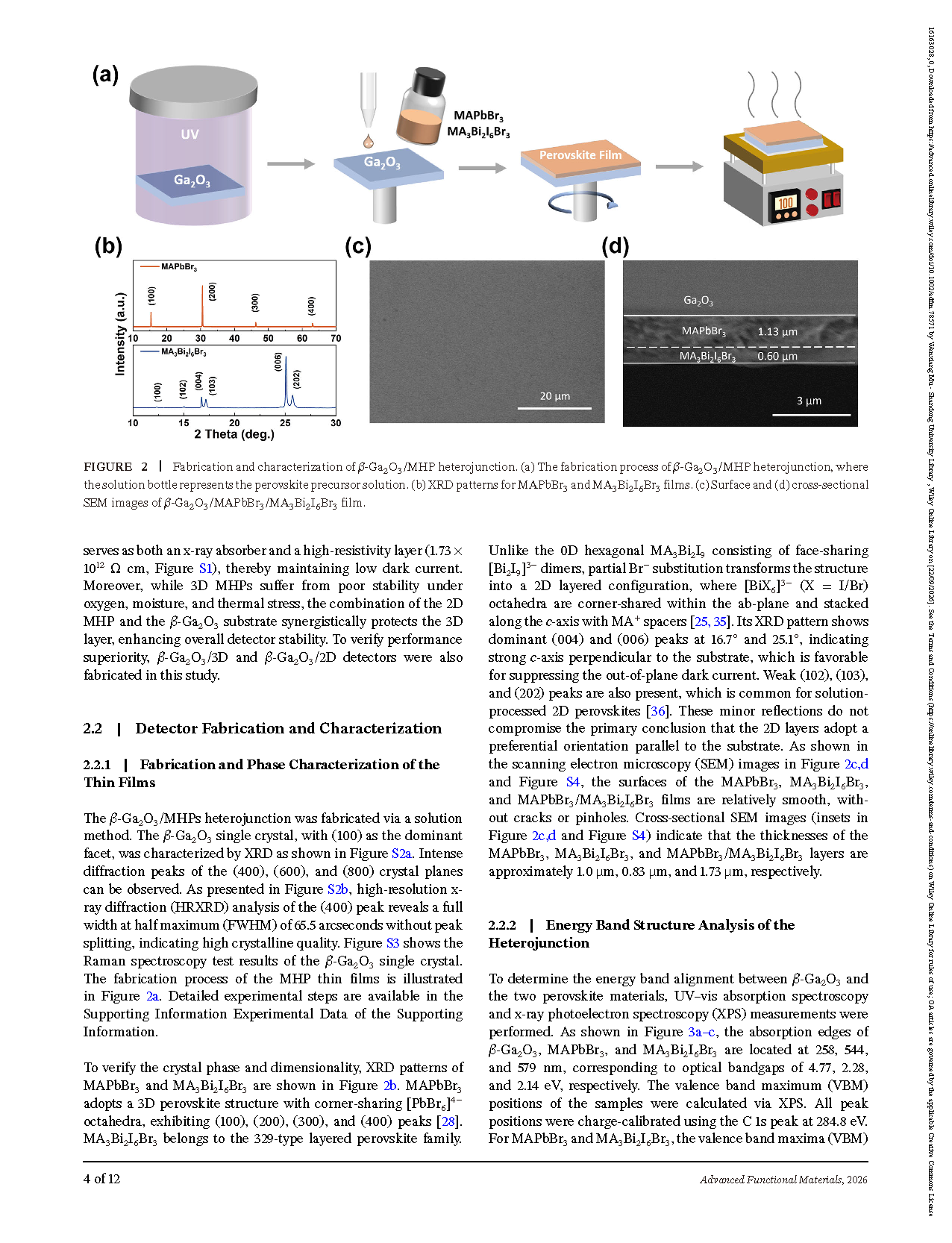
FIGURE 3. Optical characterization and band alignment of β-Ga₂O₃, MAPbBr₃ and MA₃Bi₂I₆Br₃. The transmission spectrum, UV–vis absorption spectra, and Tauc plot curves (inset) of (a) β-Ga₂O₃, (b) MAPbBr₃ and (c) MA₃Bi₂I₆Br₃. XPS valence band spectra for (d) β-Ga₂O₃, (e) MAPbBr₃, and (f) MA₃Bi₂I₆Br₃. (g) Schematic diagrams of the band alignment of β-Ga₂O₃/MAPbBr₃/MA₃Bi₂I₆Br₃. The carrier transfer process of the β-Ga₂O₃/MAPbBr₃/MA₃Bi₂I₆Br₃ at x-rays under (h) zero bias and (i) positive bias.
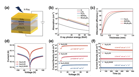
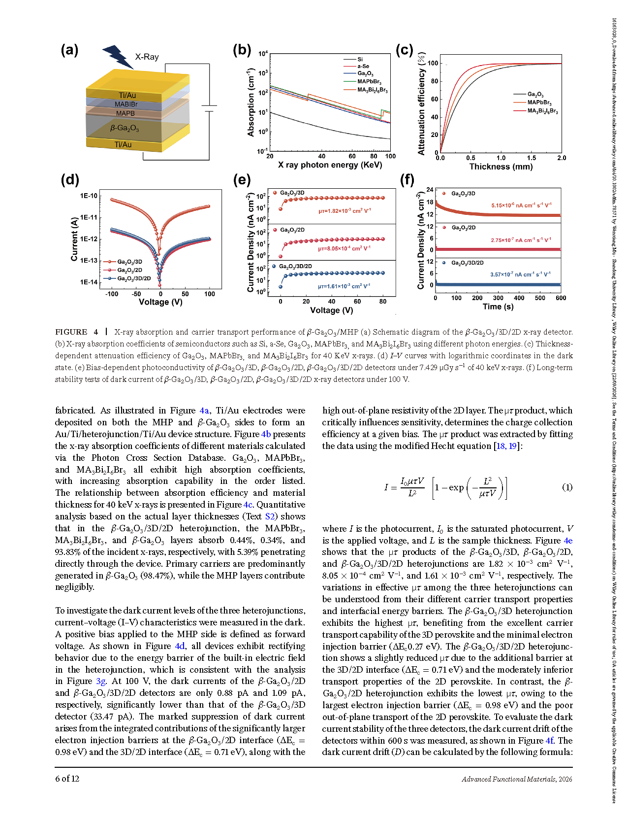
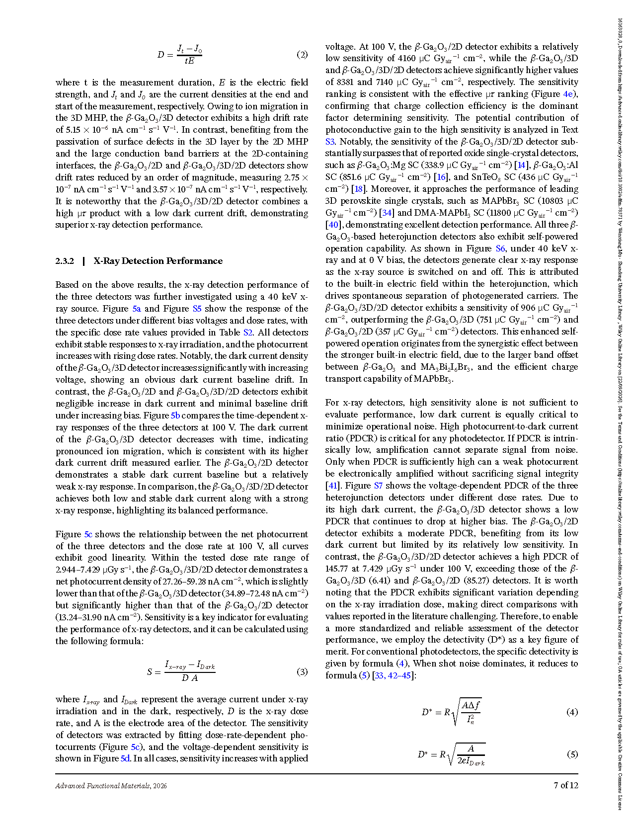
FIGURE 4. X-ray absorption and carrier transport performance of β-Ga₂O₃/MHP. (a) Schematic diagram of the β-Ga₂O₃/3D/2D x-ray detector. (b) X-ray absorption coefficients of semiconductors such as Si, a-Se, Ga₂O₃, MAPbBr₃, and MA₃Bi₂I₆Br₃ using different photon energies. (c) Thickness-dependent attenuation efficiency of Ga₂O₃, MAPbBr₃, and MA₃Bi₂I₆Br₃ for 40 KeV x-rays. (d) I-V curves with logarithmic coordinates in the dark state. (e) Bias-dependent photoconductivity of β-Ga₂O₃/3D, β-Ga₂O₃/2D, β-Ga₂O₃/3D/2D detectors under 7.429 µGy s⁻¹ of 40 keV x-rays. (f) Long-term stability tests of dark current of β-Ga₂O₃/3D, β-Ga₂O₃/2D, β-Ga₂O₃/ 3D/2D x-ray detectors under 100 V.
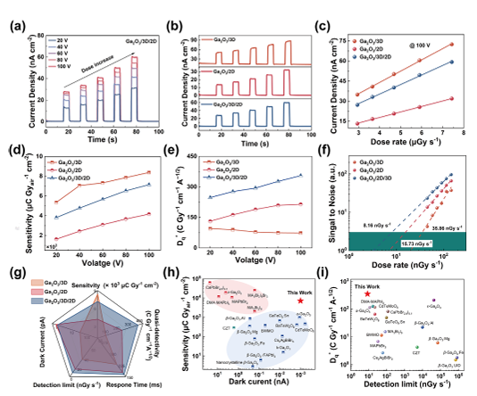
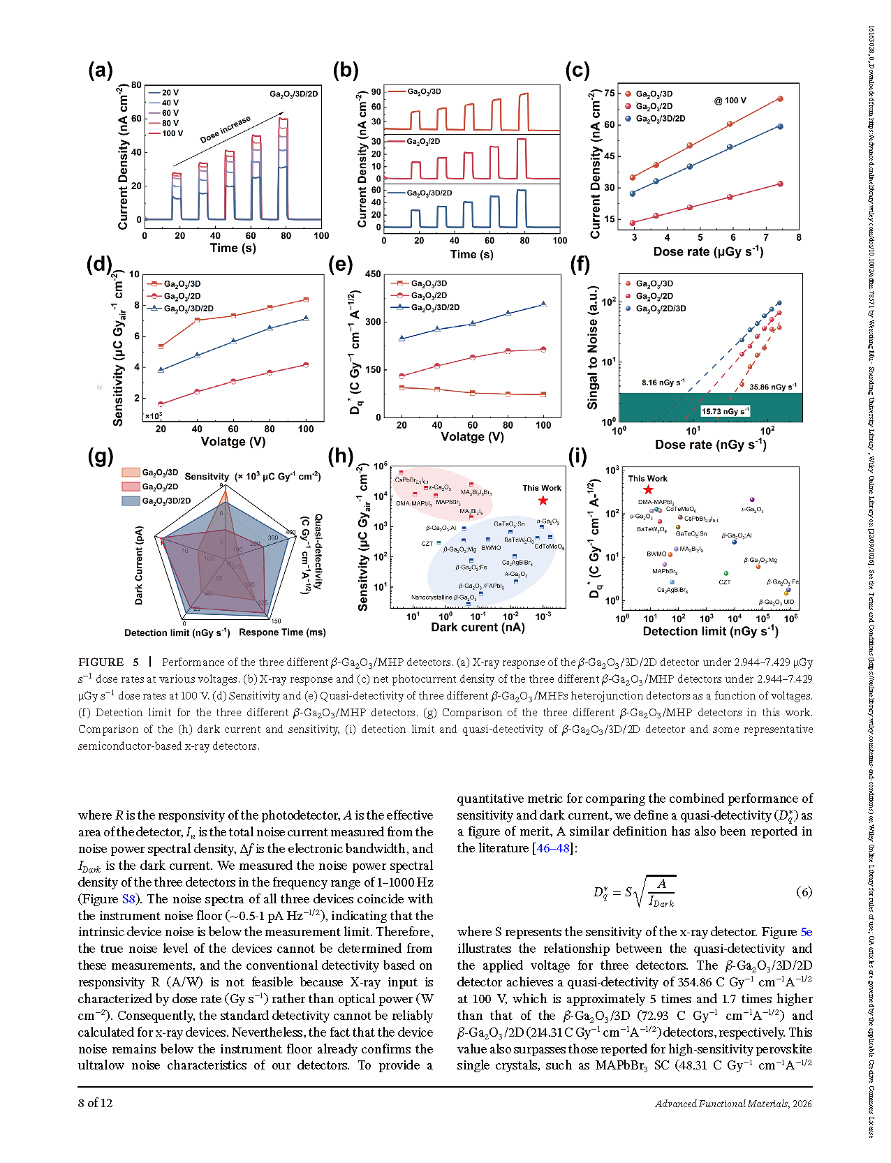
FIGURE 5. Performance of the three different β-Ga₂O₃/MHP detectors. (a) X-ray response of the β-Ga₂O₃/3D/2D detector under 2.944–7.429 µGy s⁻¹ dose rates at various voltages. (b) X-ray response and (c) net photocurrent density of the three different β-Ga₂O₃/MHP detectors under 2.944–7.429 µGy s⁻¹ dose rates at 100 V. (d) Sensitivity and (e) Quasi-detectivity of three different β-Ga₂O₃/MHPs heterojunction detectors as a function of voltages. (f) Detection limit for the three different β-Ga₂O₃/MHP detectors. (g) Comparison of the three different β-Ga₂O₃/MHP detectors in this work. Comparison of the (h) dark current and sensitivity, (i) detection limit and quasi-detectivity of β-Ga₂O₃/3D/2D detector and some representative semiconductor-based x-ray detectors.
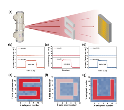
FIGURE 6. X-ray imaging of β-Ga₂O₃/3D, β-Ga₂O₃/2D, β-Ga₂O₃/3D/2D detectors. (a) Schematic diagram of the x-ray imaging system and the planar array detector. (b-d) X ray response of the β-Ga₂O₃/3D, β-Ga₂O₃/2D, β-Ga₂O₃/3D/2D detector. (e-g) The x-ray image for β-Ga₂O₃/3D, β-Ga₂O₃/2D, β-Ga₂O₃/3D/2D detector under 40 keV x-rays. The current density scale span for each image is 35 nA cm⁻².
DOI:
doi.org/10.1002/adfm.78571
Instruction
Official Account

Cooperation
Top
