


Researchers from the Sun Yat-sen University have published a dissertation titled "Deep-mesa-terminated β-Ga₂O₃ Junction Barrier Schottky Diodes with Suppressed Reverse Leakage Current" in Journal of Semiconductors.
Background
Ultra-wide bandgap (UWBG) semiconductors are at the forefront of next-generation power electronics, with monoclinic gallium oxide (β-Ga2O3) emerging as a particularly promising candidate. Its ultra-high theoretical Baliga’s figure of merit (~3444×that of Si), combined with the availability of large-area, low-cost native substrates grown from the melt, offers unprecedented potential for high-voltage, high-efficiency power devices[2]. Among these, Schottky barrier diodes (SBDs) based on β-Ga2O3 have attracted significant attention due to their simple fabrication process and fast switching characteristics. However, despite rapid progress in material quality and device processing, the performance of β-Ga2O3 SBDs—particularly in practical large-area implementations—remains fundamentally limited by excessive reverse leakage currents, which severely constrain the achievable breakdown voltage (BV).
This leakage current originates from two distinct mechanisms: (i) leakage through the Schottky barrier, dominated by trap-assisted tunneling and field-enhanced Schottky-barrier tunneling, arising from the relatively modest Schottky barrier height and high electric field at the metal/β-Ga2O3 interface[4]; and (ii) edge-related leakage, caused by severe electric-field crowding at the anode periphery, which triggers premature breakdown—particularly in large-area devices[5]. To address the first mechanism, the junction barrier Schottky (JBS) architecture has been widely adopted, in which embedded p-type regions beneath the anode provide electrostatic shielding to suppress tunneling without significantly degrading forward conduction. Meanwhile, edge termination techniques—such as field plates (FPs), junction termination extensions (JTEs), and mesa structures—have been employed to mitigate electric-field crowding.
Abstract
This work reports deep-mesa-terminated β-Ga2O3 junction barrier Schottky (Mesa-JBS) diodes that achieve high breakdown voltage (BV) and ultralow reverse leakage current. The proposed architecture integrates a micron-scale deep mesa termination to suppress edge-induced leakage current with a buried p-NiO heterojunction beneath the anode to electrostatically suppress Schottky barrier tunneling, thereby mitigating both edge-related and Schottky-barrier tunneling leakage pathways. Small-area devices (0.2 × 0.2 mm2) exhibit a BV of 1.96 kV with a reverse leakage current density below 10–5 A/cm2 at 1 kV. To demonstrate scalability, large-area Mesa-JBS diodes (2×2 mm2) were fabricated and packaged for high-current operation. These devices deliver a forward current of 3.8 A at 3 V while sustaining a BV of up to 1.2 kV, with reverse leakage currents below 20 nA (approximately 1×10⁻⁶ A/cm2) at 1 kV. These results establish deep-mesa-terminated JBS diodes as a promising and scalable solution for high-voltage, low-loss β-Ga2O3 power rectifiers.
Highlights
① Proposes a Deep-Mesa JBS synergistic structure, integrating a >1 μm deep mesa terminal with an embedded p-NiO heterojunction to simultaneously suppress Schottky barrier tunneling and edge electric field concentration.
② Achieves 2 kV breakdown voltage in small-area devices; a 0.2×0.2 mm² device demonstrates BV = 2 kV and leakage current density < 1×10⁻⁵ A/cm² at 1 kV.
③ The device maintains low Ron,sp while enhancing BV and reducing reverse leakage, achieving a favorable trade-off between high voltage capability and low conduction loss.
Conclusion
In summary, deep-mesa-terminated β-Ga2O3 JBS diodes have been successfully demonstrated with simultaneous suppression of Schottky-barrier tunneling and edge-related reverse leakage. The co-engineered architecture—combining a micron-scale deep mesa termination and a buried p-NiO heterojunction—enables high breakdown voltage and ultralow off-state loss. Small-area devices achieve a 1.96-kV BV with reverse leakage below 1×10⁻⁵ A/cm2 at 1 kV, while packaged large-area diodes deliver 3.8 A at 3 V and sustain up to 1.2 kV with leakage as low as 1×10⁻⁶ A/cm2. These results establish the Mesa-JBS architecture as a scalable and robust pathway toward high-voltage, high-current β-Ga2O3 power rectifiers for next-generation energy-efficient systems.
Project Support
This work was supported in part by the National Key Research and Development Program of China under Grant 2024YFE0205300; in part by the National Natural Science Foundation of China under Grant 62471504; in part by the Shenzhen institutions of stability support project 20231127- 114207001; in part by the High-level talent start-up funding project RC2024-008; in part by the Open Fund of the State Key Laboratory of Optoelectronic Materials and Technologies (Sun Yat-sen University) OEMT-2023-KF-05.
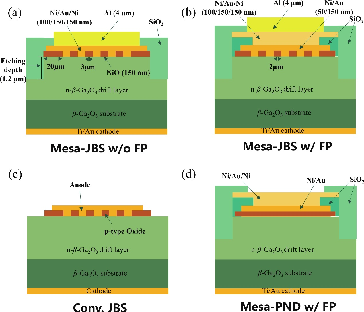
Fig. 1. Cross-sectional schematics of (a) the proposed β-Ga2O3 Mesa-JBS diode without, (b) with field plate, (c) conventional JBS, and (d) Mesa-PND with field plate.
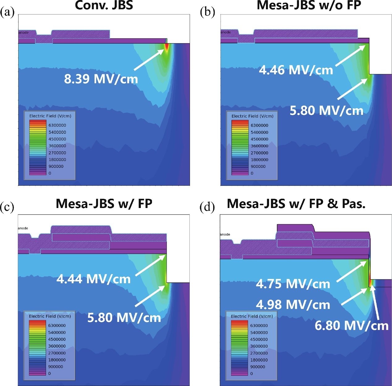
Fig. 2. Simulated electric field distribution of different device configurations under the same reverse voltage of –1.5 kV. (a) Conventional JBS; the maximum electric field (Emax) is 8.39 MV/cm in β-Ga2O3. (b) Mesa-JBS diode without SiO2 FP; Emax is 5.8 MV/cm at β-Ga2O3 trench corner. (c) Mesa-JBS diode with SiO2 FP; Emax is 5.8 MV/cm at β-Ga2O3 trench corner. (d) Mesa-JBS diode with SiO2 FP and passivation; Emax is 6.8 MV/cm in SiO2.
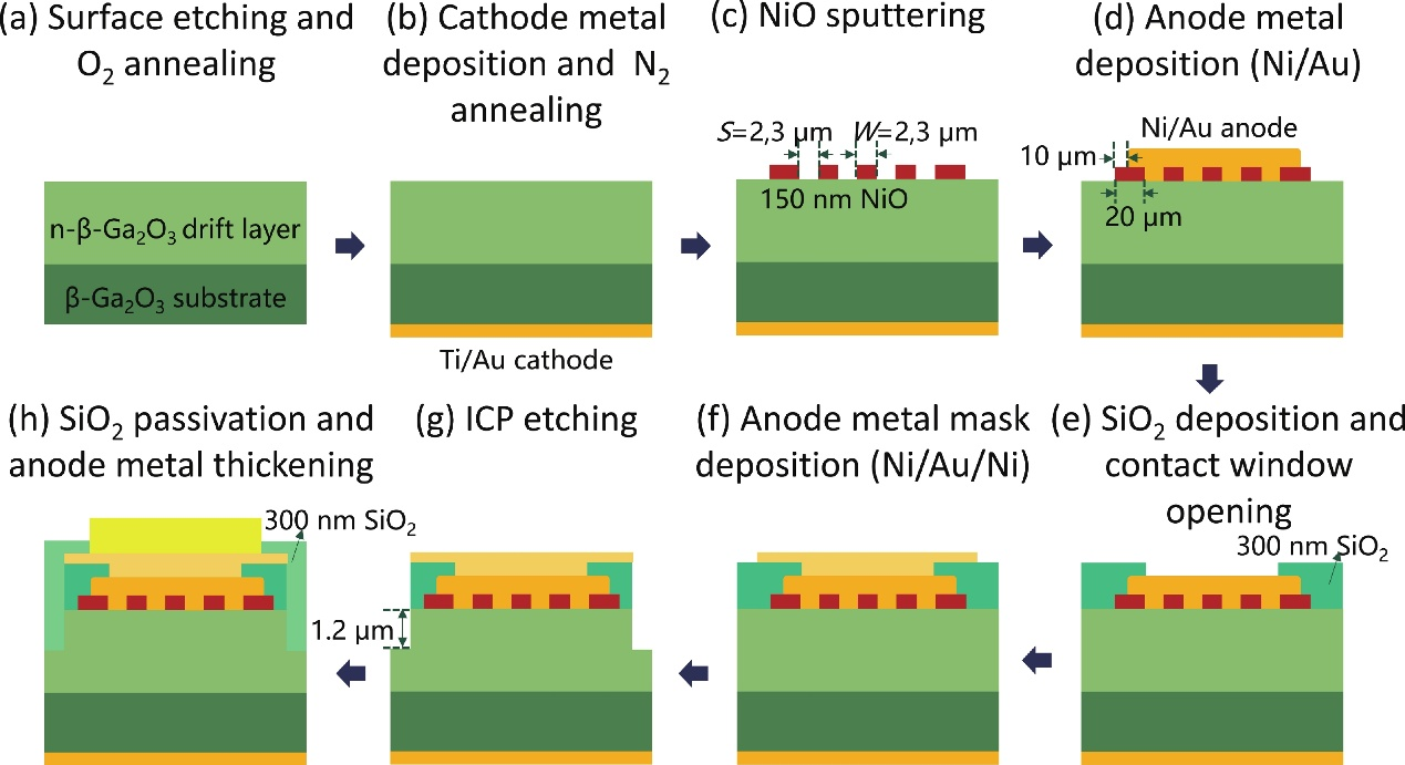
Fig. 3. Fabrication process flow of the proposed β-Ga2O3 Mesa-JBS diodes.
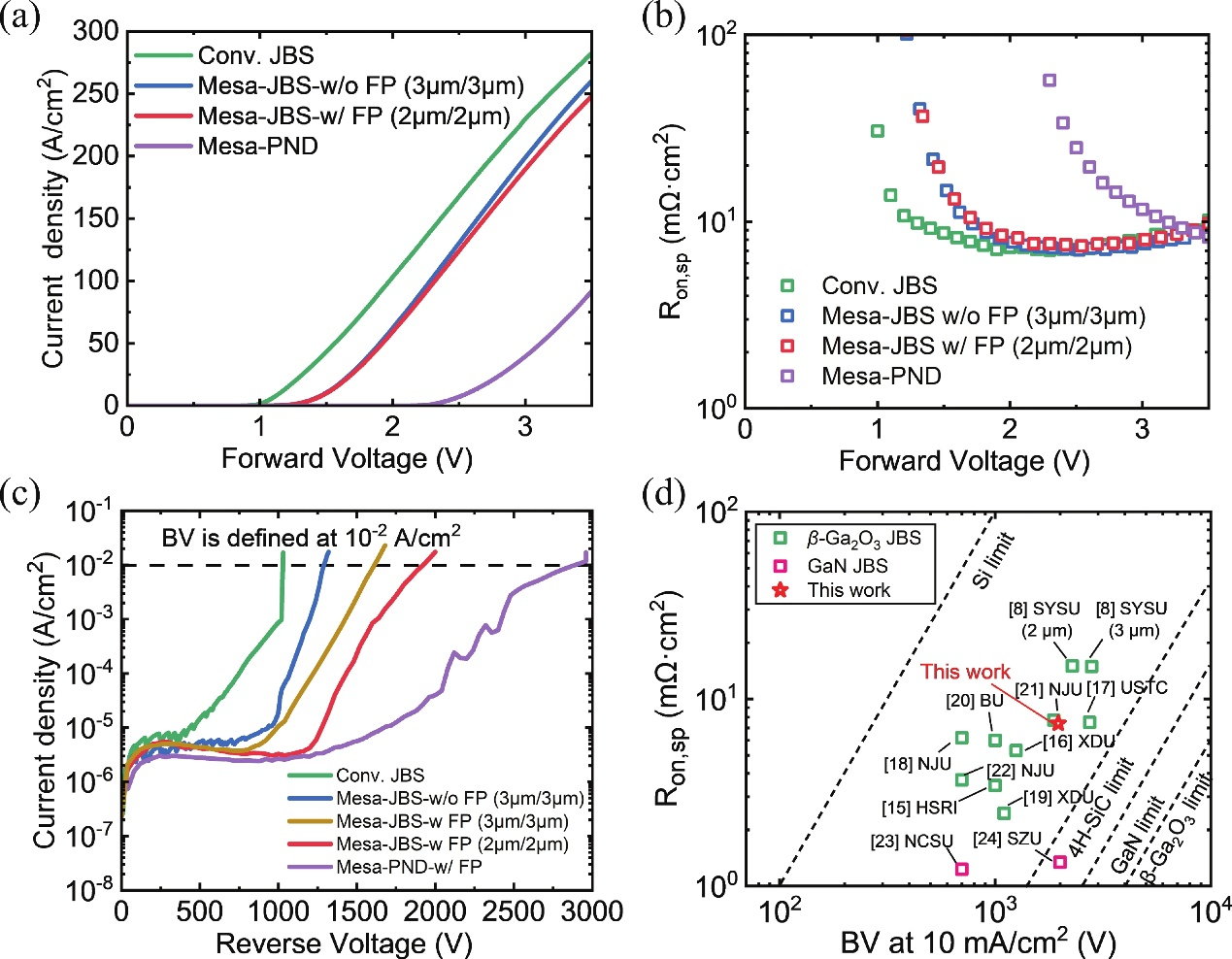
Fig. 4. (a) Linear-scale IF-VF characteristics and (b) extracted Ron,sp of the fabricated small-area conventional JBS, Mesa-JBS, and Mesa-PND diodes. (c) Comparison of IR–VR characteristics for these small-area diodes. (d) benchmark plot of Ron,sp versus BV (defined at a leakage current density of 10 mA/cm2) for reported small-area (<0.5×0.5 mm2) β-Ga2O3 and GaN JBSs.
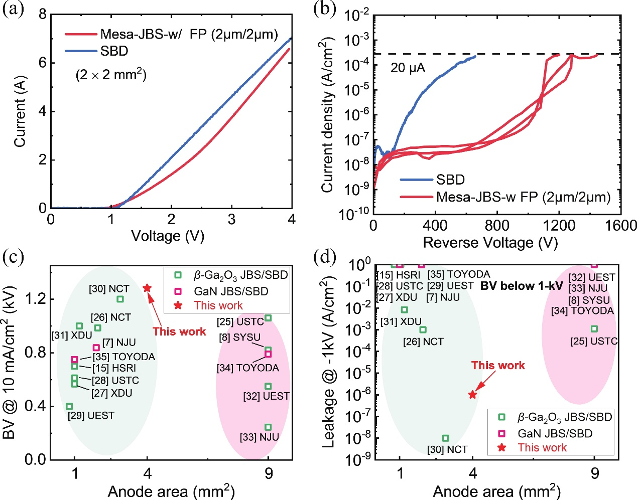
Fig. 5. (a) Linear-scale IF-VF and (b) IR–VR characteristics of the fabricated large-area Mesa-JBS diode with a SiO2 FP, compared with a conventional β-Ga2O3 SBD under the same area. (c) BV (defined at a leakage current density of 10 mA/cm2) versus anode area for the reported large-area β-Ga2O3 and GaN diodes (>0.9×0.9 mm2). (d) Reverse leakage currents (at –1 kV) of these diodes as a function of anode area.
DOI:
doi.org/10.1088/1674-4926/26050007
Instruction
Official Account

Cooperation
Top
