


A research team from Xidian University has reported a crystalline (AlGa)2O3-cap engineering approach for improving the interface quality and electrical performance of β-Ga2O3 MOS devices. The work, entitled “Improved Interface Quality in β-Ga2O3 MOSFETs With a Crystalline (AlGa)2O3 Cap,” was published in IEEE Transactions on Electron Devices. The corresponding authors are Yibo Wang and Genquan Han.
Background
β-Ga2O3 is considered a promising ultrawide-bandgap semiconductor for next-generation power electronics because of its high critical electric field and the availability of native substrates.
However, β-Ga2O3 lacks a high-quality native oxide. Therefore, foreign high-k dielectrics such as Al2O3 are typically employed to construct MOS gate stacks. Direct contact between amorphous Al2O3 and crystalline β-Ga2O3 can introduce incomplete bonding and structural disorder during the initial dielectric-growth stage, resulting in interface traps, near-interface oxide traps, and dielectric-related defects.
These defects can degrade subthreshold characteristics and channel transport, induce threshold-voltage instability, and increase gate leakage. Improving the dielectric/β-Ga2O3 interface therefore remains essential for achieving high-performance and reliable β-Ga2O3 MOS power devices.
In this work, a crystalline (AlGa)2O3 cap layer was introduced between the amorphous Al2O3 dielectric and β-Ga2O3, providing a structurally improved transition layer at the MOS interface.
Abstract
A ~5-nm Al2O3 layer was first deposited on β-Ga2O3 by ALD, followed by annealing at 1000 °C for 3 min in N2. A 25-nm Al2O3 layer was subsequently deposited to complete the gate stack. Interfacial Ga-Al interdiffusion during annealing transformed the initially deposited layer into an approximately 5-nm-thick crystalline (AlGa)2O3 cap.
Cross-sectional HRTEM revealed an epitaxial-like alignment between the crystalline cap and the underlying β-Ga2O3. Elemental mapping further confirmed Ga-Al interdiffusion at the interface.
MOS capacitor measurements showed a pronounced reduction in interface traps after introducing the crystalline cap. The capped MOSCAPs also exhibited lower gate leakage and higher breakdown fields over the investigated temperature range, demonstrating improved overall gate-stack quality.
For β-Ga2O3 MOSFETs, the representative hysteresis was reduced from 0.57 to 0.43 V, while the subthreshold swing was improved from 909 to 734 mV/dec. The specific ON-resistance decreased from 46.2 to 38.8 mΩ·cm2. Statistical measurements on 12 devices in each group confirmed reductions of approximately 32% in hysteresis and 16% in SS.
The capped MOSFETs also exhibited lower OFF-state leakage and improved breakdown characteristics. Combined with the reduced ON-resistance, the power figure of merit increased from 95.5 to 136.3 MW/cm2, corresponding to a 42.7% enhancement.
Positive-bias instability measurements further demonstrated suppressed electron trapping. The capped devices exhibited smaller threshold-voltage shifts over the investigated stress-time and gate-bias ranges. A ΔVTH of only 0.82 V after 1000 s at VG,stress = 4 V was obtained, indicating improved threshold-voltage stability.
Highlights
The key innovation of this work lies in the use of a crystalline oxide transition layer instead of relying solely on direct optimization of the amorphous dielectric/semiconductor interface.
Through thin-Al2O3 predeposition and high-temperature PDA, a crystalline (AlGa)2O3 cap with epitaxial-like alignment to β-Ga2O3 was formed in situ. This approach reduces direct contact between amorphous Al2O3 and β-Ga2O3 and suppresses interface-related defects.
More importantly, the improved interface quality was consistently verified from structural characterization and MOSCAP measurements to transistor performance and bias-stress reliability. The resulting devices achieved simultaneous improvements in hysteresis, subthreshold swing, channel transport, breakdown performance, PFOM, and threshold-voltage stability.
Conclusion
A crystalline (AlGa)2O3 cap was successfully introduced into β-Ga2O3 MOS gate stacks through thin Al2O3predeposition followed by high-temperature PDA.
The crystalline cap suppresses interface defects and electron trapping, improves the overall gate-stack quality, and leads to enhanced subthreshold characteristics, channel transport, breakdown performance, PFOM, and positive-bias stability.
These results demonstrate that crystalline oxide interfacial engineering provides an effective route toward high-performance and reliable β-Ga2O3 MOS power devices.
Project Support
This work was supported by the National Key Research and Development Program of China, the National Natural Science Foundation of China, the Key Program of Shaanxi Provincial Department of Science and Technology, the Key Program of Hangzhou City Department of Science and Technology, the Zhejiang Provincial Natural Science Foundation of China, the Leading Innovation and Entrepreneurship Project of Zhejiang Province, and the Hangzhou Leading Talent Program.
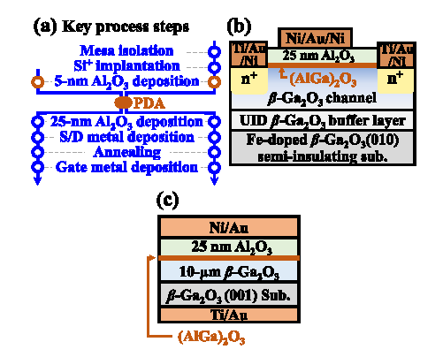
Fig. 1. Key fabrication steps and schematic structures of β-Ga2O3 MOSFETs and MOSCAPs incorporating the crystalline (AlGa)2O3 cap.
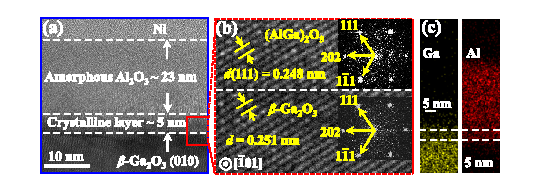
Fig. 2. TEM and HRTEM images of the Al2O3/crystalline-(AlGa)2O3/β-Ga2O3 gate stack and corresponding Ga and Al elemental maps.
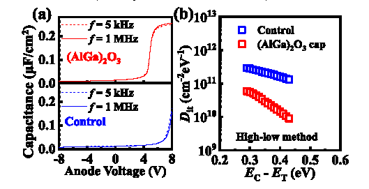
Fig. 3. High- and low-frequency C-V characteristics and extracted interface-trap density of MOSCAPs with and without the crystalline (AlGa)2O3 cap.
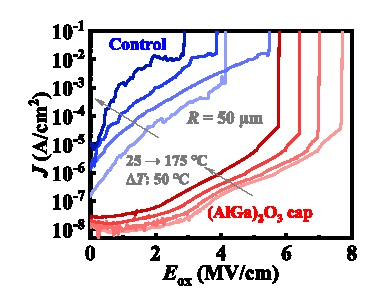
Fig. 4. Temperature-dependent J-E characteristics of MOSCAPs with and without the crystalline cap.
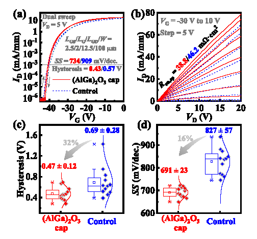
Fig. 5. Transfer and output characteristics of β-Ga2O3 MOSFETs and statistical distributions of hysteresis and subthreshold swing.
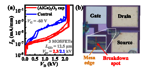
Fig. 6. OFF-state breakdown characteristics and post-breakdown optical image of the MOSFET.
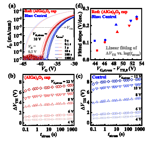
Fig. 7. Evolution of transfer characteristics and threshold-voltage shift under positive gate-bias stress.
DOI:
doi.org/10.1109/TED.2026.3716668
Instruction
Official Account

Cooperation
Top
