


A research paper titled “The defect-related anisotropic strain induced saw-like cracking in the (001) β-Ga₂O₃ homoepitaxial film” has recently been published in Applied Surface Science by the group of Professor Hongwei Liang and Associate Professor Hezhi Zhang at the School of Integrated Circuits, Dalian University of Technology, in collaboration with the State Key Laboratory of Crystal Materials, Shandong University. This work reveals the lattice distortion characteristics beneath streaky groove defects in (001) β-Ga₂O₃ homoepitaxial films, and explains how defect-induced anisotropic strain causes saw-like cracking in vertical SBD devices.
Background
β-Ga2O3, as an ultra-wide bandgap (UWBG) semiconductor material, exhibits a bandgap of 4.8–4.9 eV, a theoretical breakdown electric field as high as 8 MV/cm, and a Baliga figure of merit (BFOM) of 3444, demonstrating tremendous potential in power electronic devices, deep-ultraviolet photodetectors, and extreme-environment applications. However, during the epitaxial growth of β-Ga2O3, defects that extend from the substrate into the epitaxial layer and those generated during the epitaxial process not only act as non-radiative recombination centers, reducing carrier lifetime, but also deteriorate the surface quality of the epitaxial layer, leading to a reduced breakdown voltage and compromised long-term operational reliability of power devices. Therefore, a deep understanding of the intrinsic relationships among stress accumulation, lattice distortion, defect generation, and surface morphology evolution in β-Ga2O3 epitaxial layers is critically important for optimizing epitaxial processes and improving device performance.
Abstract
1.Markedly reduced carrier lifetime in the streaky groove region
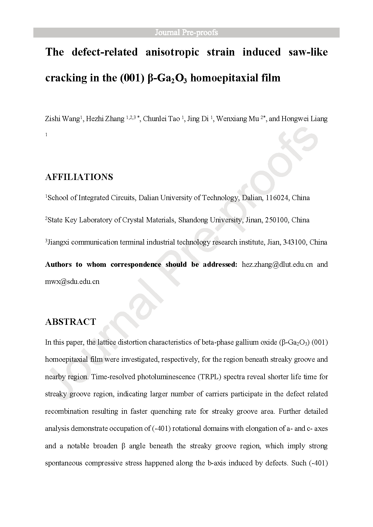
The homoepitaxial film was grown on a Sn-doped β-Ga2O3 (001) substrate by the oxide vapor phase epitaxy (OVPE) method. Scanning electron microscopy (SEM) characterization revealed streaky groove defects elongated along the [010] direction on the (001) epitaxial layer surface. The photoluminescence (PL) spectra demonstrate that the deep-level emission peak positions in the streaky groove region are essentially identical to those in the nearby region (350, 385 and 434 nm), whereas time-resolved photoluminescence (TRPL) measurements reveal that the carrier lifetimes in the groove region at all three wavelengths of 350, 385 and 434 nm are markedly shorter than those in the nearby region. This indicates that a larger number of carriers participate in the defect-related recombination in the groove region, giving rise to a faster quenching rate, which is strongly associated with self-trapped exciton emission.
2.Presence of (-401) rotational domains and pronounced anisotropic strain beneath the streaky groove
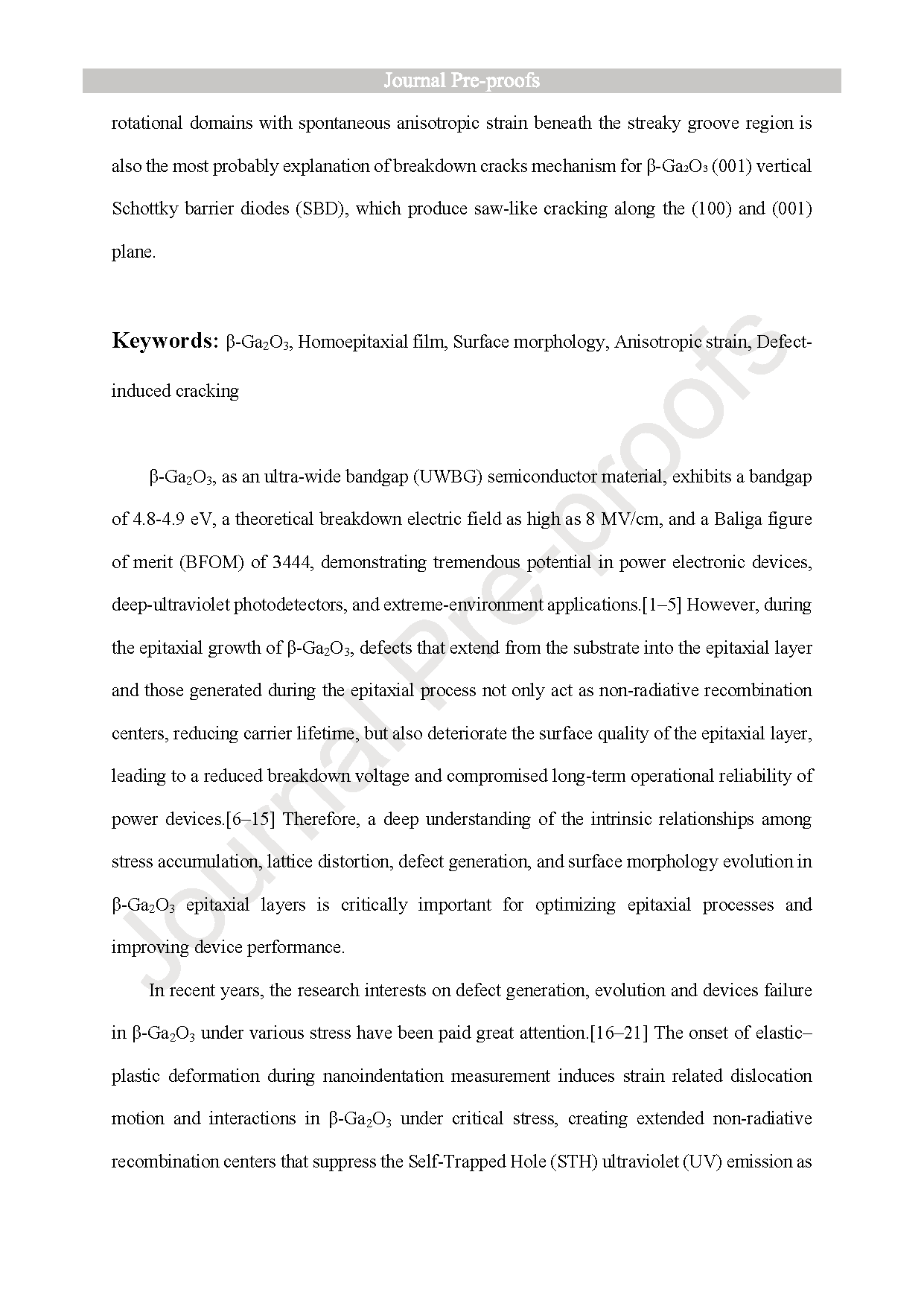
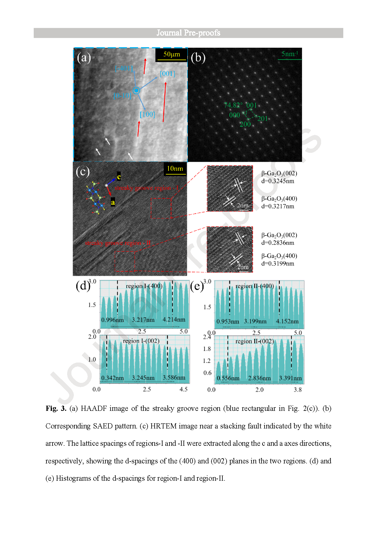
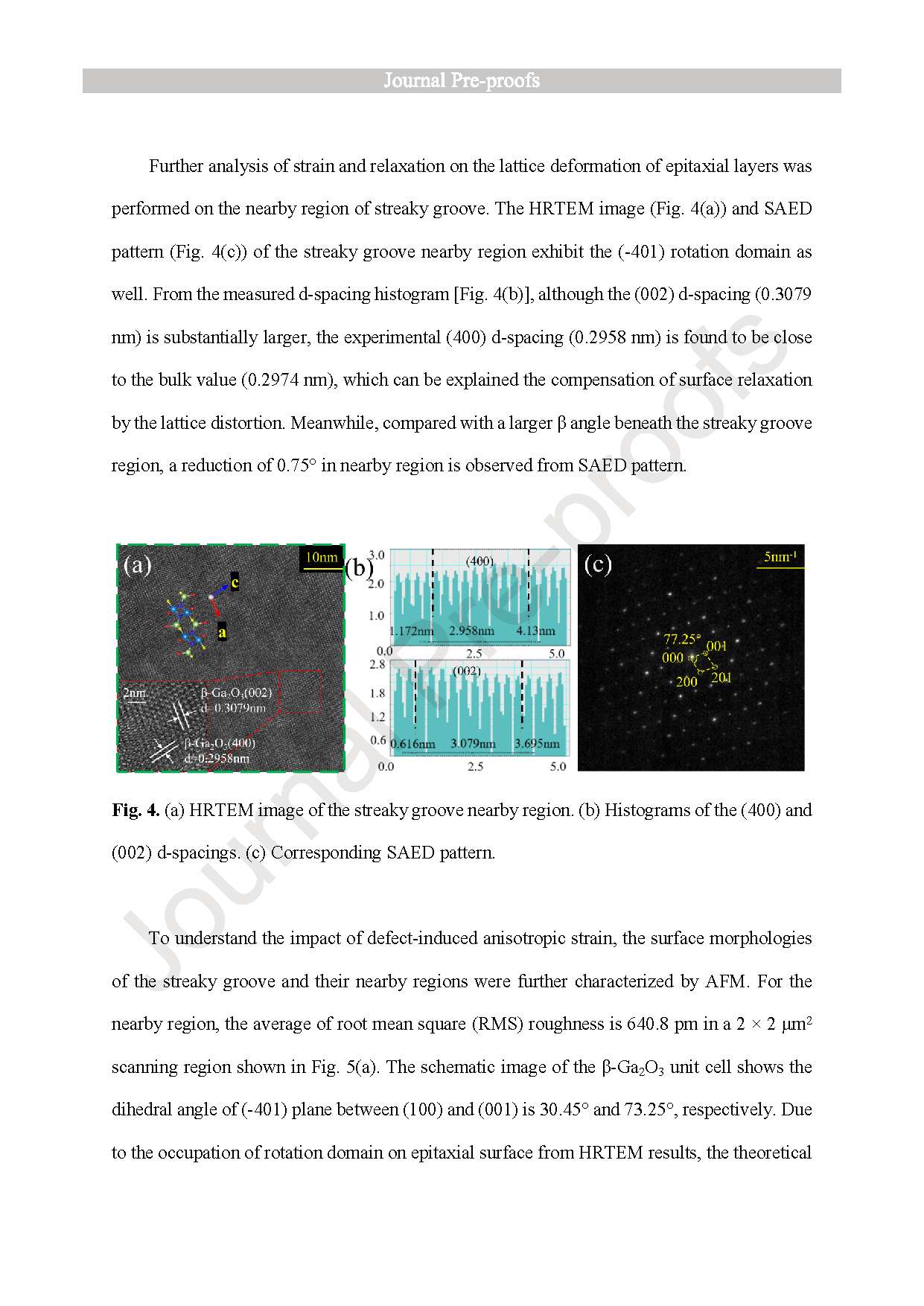
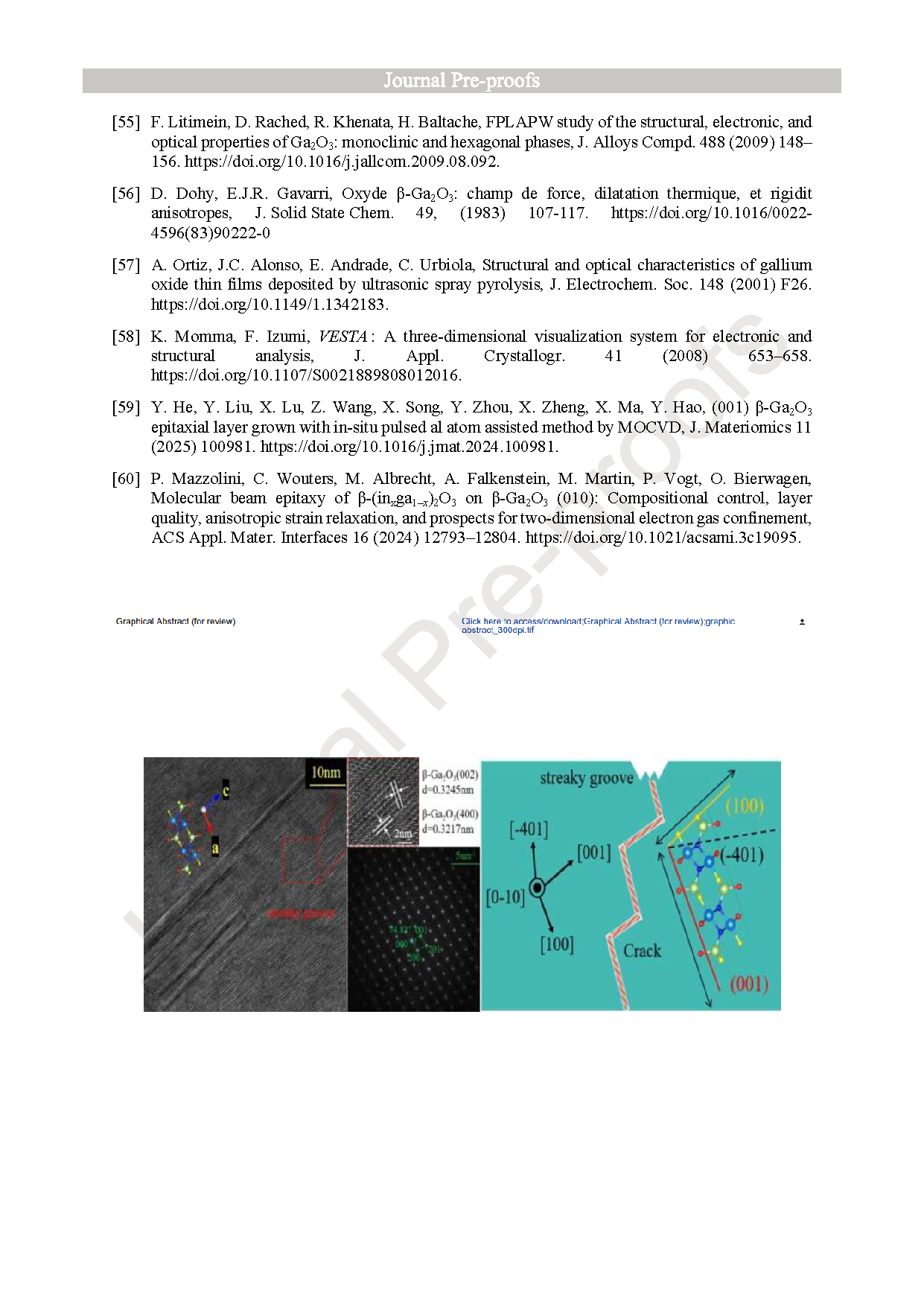
high-resolution transmission electron microscopy (HRTEM) and (SAED) analyses reveal that (-401) rotational domains are ubiquitous in both the streaky groove region and its nearby region, accompanied by stacking faults and tilted dislocation lines. The β angle of the unit cell in the region beneath the streaky groove increases to approximately 105.18°, and the (400) and (002) d-spacings along the a- and c- axes are both appreciably elongated , indicative of spontaneous compressive stress along the b-axis. In the nearby region, although (-401) rotational domains are likewise present, the (400) d-spacing remains close to the bulk value and the β angle decreases by approximately 0.75°, reflecting a considerably milder degree of lattice distortion. The specific parameters are summarized in Table I.
3.AFM verification that rotational domains give rise to an increased surface angle
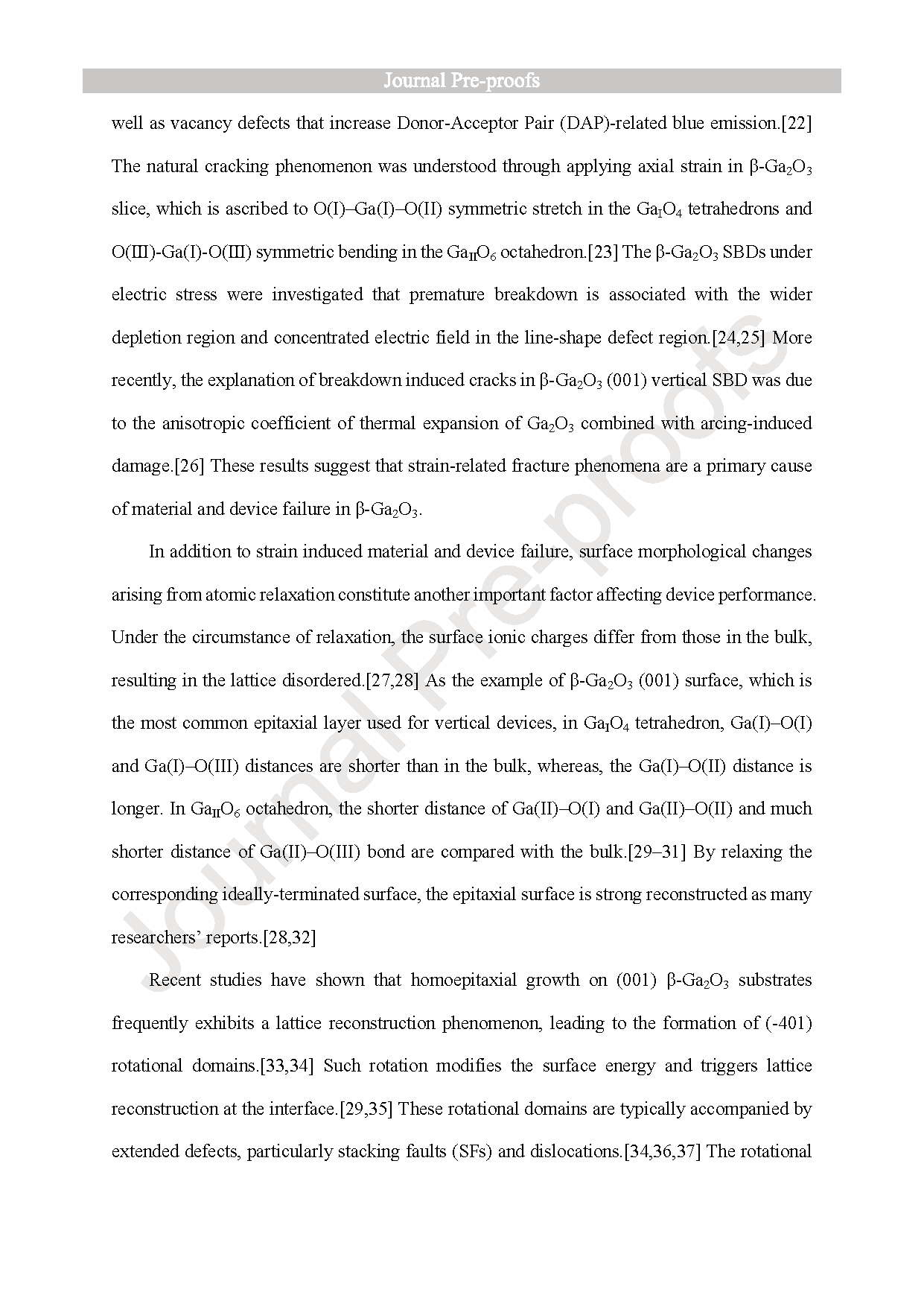
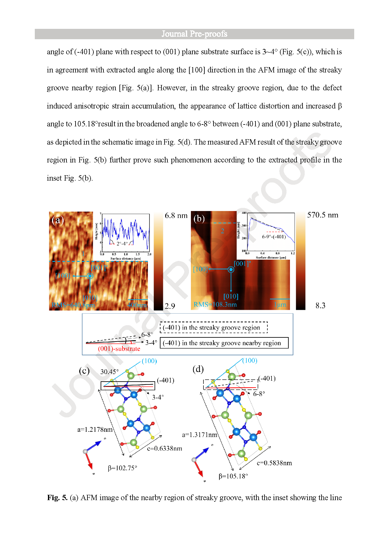
AFM characterization demonstrates that the angle between the (-401) plane and the (001) substrate surface in the nearby region is approximately 3-4°, in agreement with the theoretically calculated value, whereas this angle broadens to 6-8° in the streaky groove region. This result further corroborates that the defect-induced anisotropic strain accumulation in the groove region gives rise to more severe lattice distortion.
Highlights
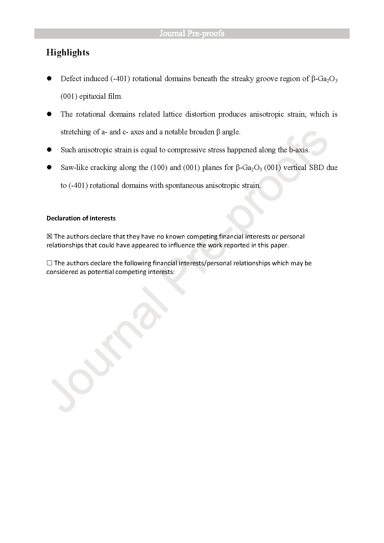
Defect induced (-401) rotational domains beneath the streaky groove region of β-Ga2O3 (001) epitaxial film.
The rotational domains related lattice distortion produces anisotropic strain, which is stretching of a- and c- axes and a notable broaden β angle.
Such anisotropic strain is equal to compressive stress happened along the b-axis.
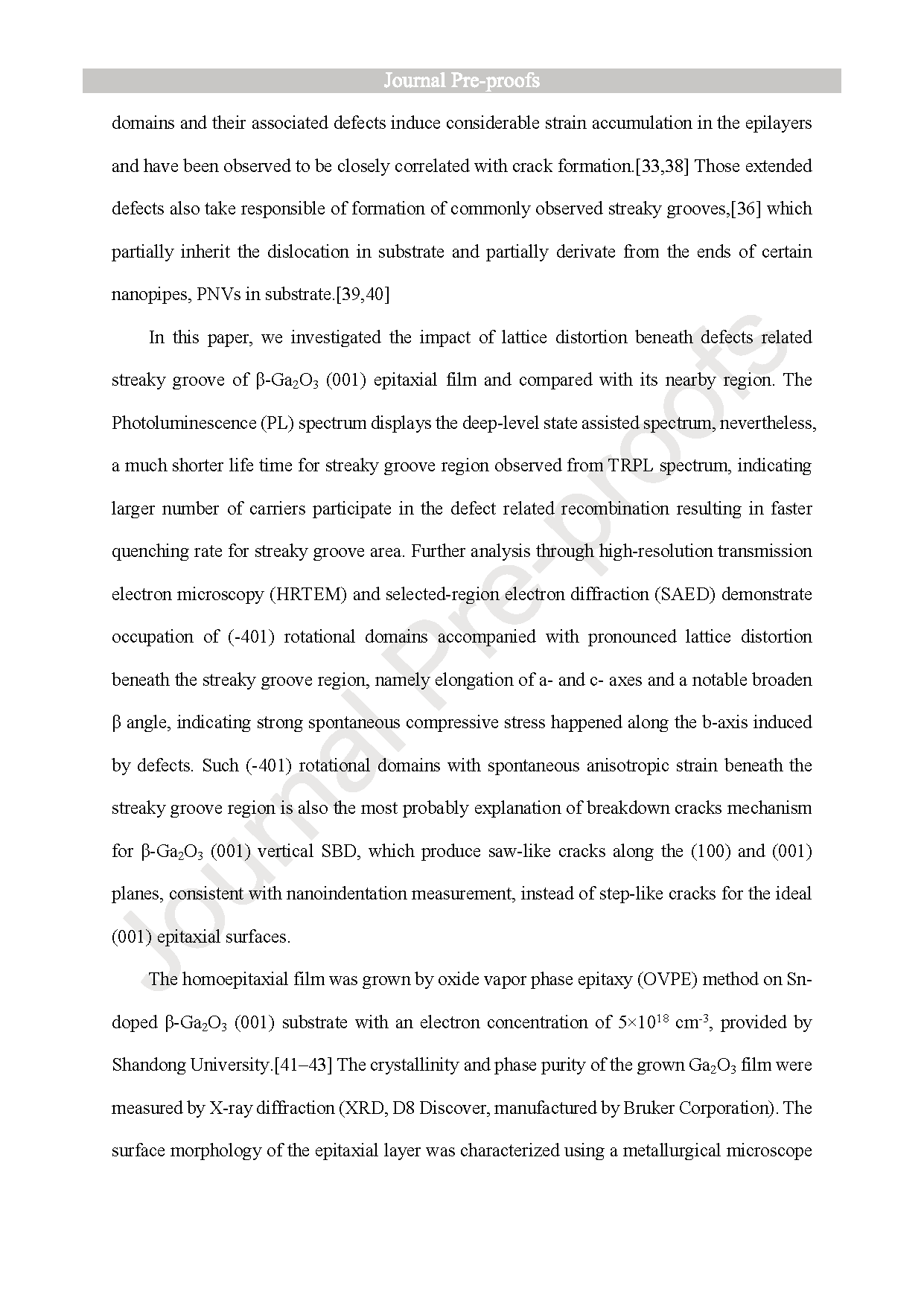
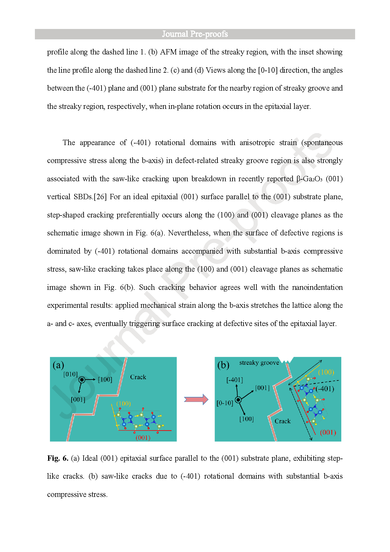
Saw-like cracking along the (100) and (001) planes for β-Ga2O3 (001) vertical SBD due to (-401) rotational domains with spontaneous anisotropic strain.
Conclusion
The present study proposes a complete physical model: the emergence of (-401) rotational domains in the streaky groove region manifests strong anisotropic strain accumulation, expressed as elongation of the a- and c- axes together with an increase in the β angle, which is equivalent to compressive stress along the b-axis. Once the accumulated stress exceeds the critical threshold, cleavage preferentially occurs along the (100) and (001) planes of the rotational domain system, ultimately giving rise to saw-like cracks. This mechanism well accounts for the recently reported phenomenon of saw-like cracking upon breakdown in β-Ga2O3 (001) vertical SBDs, and is consistent with the nanoindentation experimental results, thereby providing an important theoretical basis for optimizing epitaxial processes and enhancing device reliability.
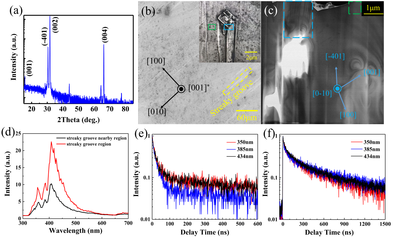
Fig. 1. (a) XRD θ-2θ pattern of the (001) β-Ga2O3 homoepitaxial film. (b) Surface morphology of the (001) β-Ga2O3 homoepitaxial layer and the detailed streaky groove in the inset. (c) BF-TEM image of the streaky groove region (blue rectangle) and the nearby region (green rectangle). (d) PL spectrum of the streaky groove and its nearby region. (e) and (f) TRPL spectra of the streaky groove and its nearby region, respectively.
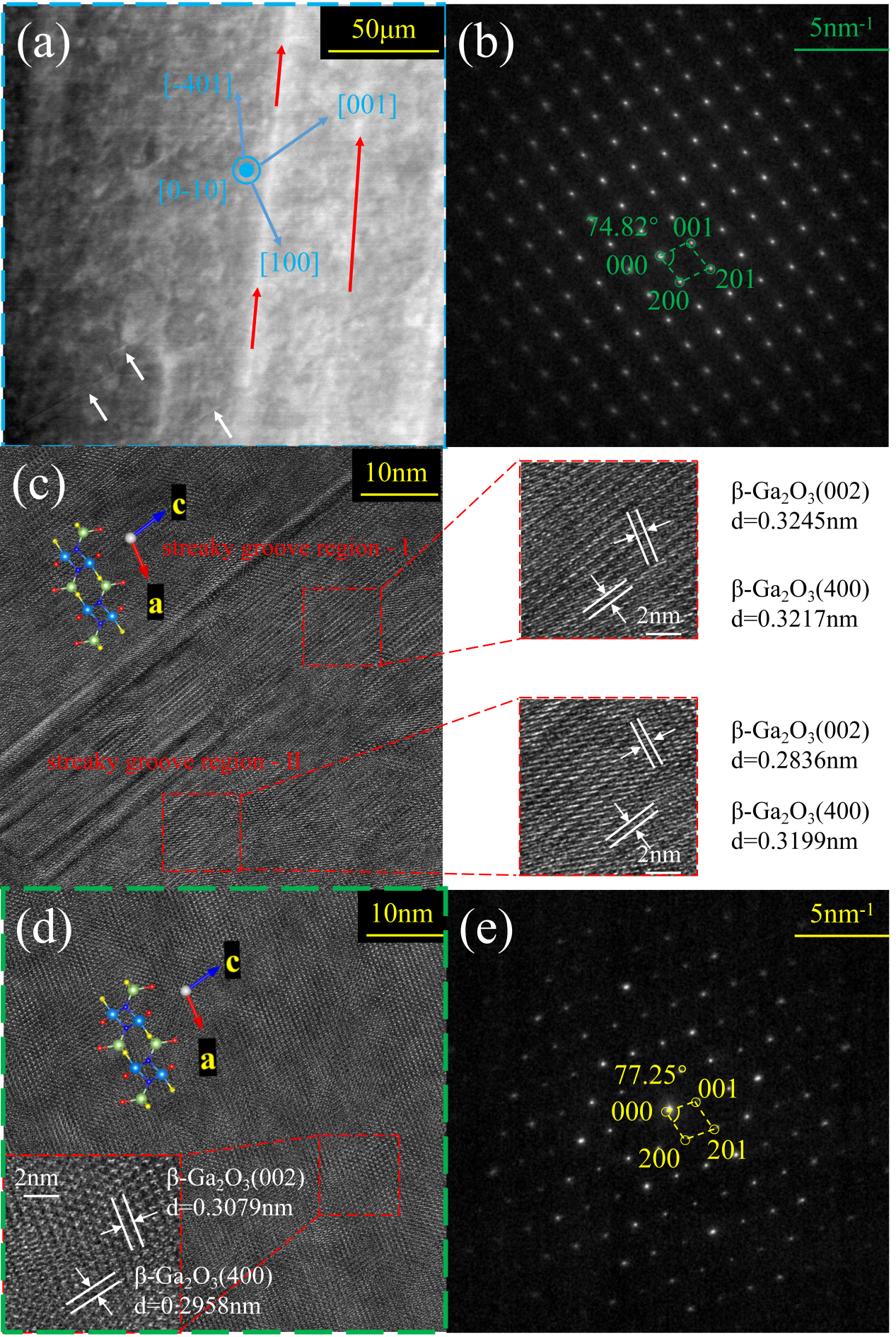
FIG. 2. (a) HAADF image of the streaky groove region (blue rectangular in Fig. 1(c)), (b) Corresponding SAED pattern, (c) HRTEM image near a stacking fault indicated by the white arrow. The lattice spacings of regions-I and -II were extracted along the c-axis and a-axis directions, respectively, showing the d-spacings of the (400) and (002) planes in the two regions. (d) HRTEM image of the streaky groove nearby region, (e) Corresponding SAED pattern.
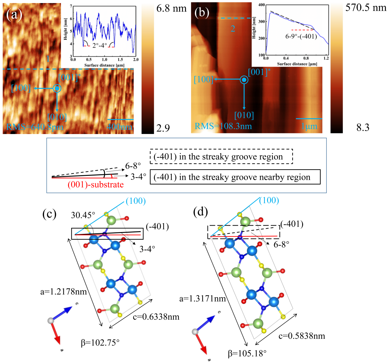
Fig. 3. (a) AFM image of the nearby region of streaky groove, with the inset showing the line profile along the dashed line 1. (b) AFM image of the streaky region, with the inset showing the line profile along the dashed line 2. (c) and (d) Views along the [0-10] direction, the angles between the (-401) plane and (001) plane substrate for the nearby region of streaky groove and the streaky region, respectively, when in‑plane rotation occurs in the epitaxial layer.
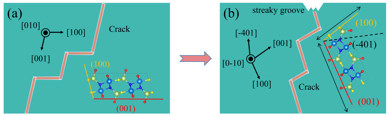
Fig. 4. (a) Ideal (001) epitaxial surface parallel to the (001) substrate plane, exhibiting step-like cracks. (b) saw-like cracks due to (-401) rotational domains with substantial b-axis compressive stress.
DOI:
doi.org/10.1016/j.apsusc.2026.168380
Instruction
Official Account

Cooperation
Top
