


In August 2022, the United States imposed technology restrictions on gallium oxide. At the time, many Chinese institutions were still working to catch up with Novel Crystal Technology, Inc. (NCT) on single-crystal substrate technology. Meanwhile, the team led by Academician Yue Hao of the School of Integrated Circuits, Xidian University, had already built up years of research experience and technical capabilities, placing China at a high starting point for pursuing technological self-reliance and self-strengthening.
This was not a matter of luck. It was the fruit of Yue Hao's forward-looking vision and proactive strategic deployment.
As a pioneer and leader in the field of third-generation (wide-bandgap) semiconductor electronics in China, Yue Hao has been working on gallium nitride (GaN)/silicon carbide (SiC) materials and microwave devices since the 1990s. He laid the theoretical and technological foundation for GaN epitaxial growth, device structures, and manufacturing processes in China's third-generation semiconductor industry.
And just as GaN was beginning to reach the international forefront, he had already turned his attention to "ultra-wide-bandgap semiconductors," represented by materials such as gallium oxide and diamond.
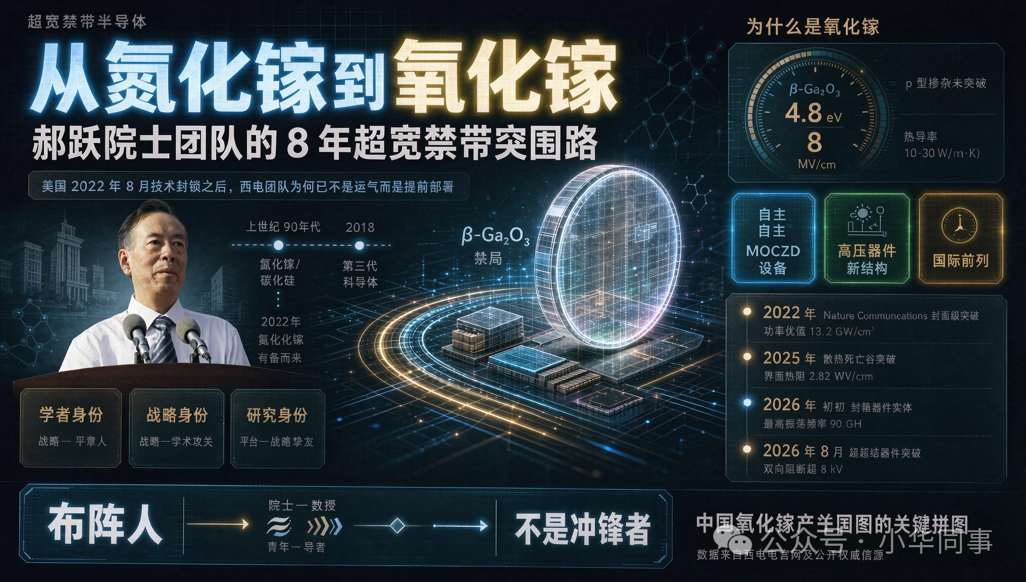
Who Is Academician Yue Hao? Three Roles That Shape His Work
To understand Academician Yue Hao's strategic focus on Ga₂O₃, it is important to first understand the three roles he has played throughout his career.
Academic Role
An academician of the Chinese Academy of Sciences and a leading expert in microelectronics, Yue Hao was born in Chongqing in 1958. He graduated from Xidian University in 1982 with a degree in Semiconductor Physics and Devices, and received his Ph.D. in Computational Mathematics from Xi'an Jiaotong University in 1991. He currently serves as Director of the School of Integrated Circuits, Xidian University, and is a doctoral supervisor in Microelectronics and Solid-State Electronics.
Strategic Role
Yue Hao has also played an important role in national science and technology planning. He has served as Leader of the Expert Group for the implementation of the National Major Science and Technology Project on "Core Electronic Components, High-End General-Purpose Chips, and Basic Software Products," Convener of the 7th Academic Discipline Appraisal Group of the Academic Degrees Committee of the State Council (for the first-level discipline of Electronic Science and Technology), Director of the Information Sciences Department of the National Natural Science Foundation of China (NSFC), and Vice President of the Chinese Institute of Electronics.
Research Role
His research focuses primarily on wide-bandgap and ultra-wide-bandgap semiconductor devices and materials, novel micro- and nanoscale semiconductor devices and their reliability, and system-on-chip (SoC) design.
His research achievements have received numerous national-level awards, including one Second-Class National Technological Invention Award (2009), two Second-Class National Science and Technology Progress Awards (2008 and 2015), one Third-Class National Science and Technology Progress Award (1998), and one First-Class National Teaching Achievement Award (2018). He received the Ho Leung Ho Lee Foundation Prize for Science and Technology in 2010 and the Shaanxi Provincial Supreme Science and Technology Award in 2019.
The combination of these three roles means that Yue Hao's work on Ga₂O₃ has never been driven solely by academic publications. Instead, it represents a systematic approach integrating national strategic priorities, platform development, and research endeavors.
Why Ga₂O₃? Yue Hao's Ultra-Wide-Bandgap Semiconductor Strategy
Yue Hao's focus on Ga₂O₃ stems from his broader understanding of the development trajectory of the semiconductor industry.
β-Ga₂O₃ has a bandgap of approximately 4.8 eV and a theoretical critical electric field of around 8 MV/cm, making it a highly promising material for next-generation high-voltage power devices. But it also has two major limitations: the absence of mature p-type doping technology and a low thermal conductivity of only about 10–30 W/(m·K), less than one-sixth that of diamond.
Yue Hao's strategy is to address these limitations through heterogeneous integration rather than focusing solely on the single-crystal route.
According to an official report by Xidian University News Network, since 2018, under the leadership of Academician Yue Hao, Xidian University has developed a series of technological innovations, including indigenously developed MOCVD equipment for Ga₂O₃ growth, high-quality Ga₂O₃ epitaxial materials, and new structures and fabrication processes for high-voltage devices. These advances have enabled rapid improvements in the performance of Ga₂O₃ power diodes and power transistors, bringing China's research in Ga₂O₃ power devices to the international forefront, according to the university.
This statement is significant for several reasons:
Indigenously developed MOCVD equipment: It means the team is not simply relying on imported equipment.
New high-voltage device structures: It indicates an effort to develop alternative device architectures rather than simply following established approaches overseas.
"International forefront": This is the wording used in Xidian University's official account.
Key Milestones in Xidian University's Ga₂O₃ Research
As representative achievements of Academician Yue Hao's research team, several milestones are particularly worth noting from an industry perspective:
2022: A Breakthrough Featured on the Cover of Nature Communications
A team led by Professor Jincheng Zhang and Professor Hong Zhou developed a p-NiO/n-Ga₂O₃ heterojunction diode. By leveraging a hole super-injection effect, the device achieved a power figure of merit (PFOM) of 13.2 GW/cm², reported as the highest value achieved to date for Ga₂O₃ semiconductor devices.
2025: Addressing Ga₂O₃'s Thermal Bottleneck
Professors Jincheng Zhang and Jing Ning introduced graphene as an interfacial "bridge" between Ga₂O₃ and diamond, enabling the two materials to be effectively integrated. The resulting thermal boundary resistance was reduced to 2.82 m²·K/GW, with the work published in Nature Communications. The breakthrough directly addresses one of the most significant barriers to the commercialization of Ga₂O₃: heat dissipation.
Early 2026: New Records in Ga₂O₃ RF Devices
Professor Jincheng Zhang's research team reported an important advance in Ga₂O₃ RF devices. The devices achieved a maximum oscillation frequency (fmax) of 90 GHz, an output power density of 4.1 W/mm at 6 GHz, and a minimum noise figure of 0.48 dB at 8 GHz. The work was published as a cover paper in Science Advances.
August 2026: Breakthrough in Dual-Superjunction Devices
Academician Yue Hao, Professor Jincheng Zhang, and Professor Hong Zhou, together with Researcher Xiaodong Zhang of the Suzhou Institute of Nano-Tech and Nano-Bionics, Chinese Academy of Sciences, reported a p-NiO/n-Ga₂O₃ dual-superjunction MOS junction field-effect transistor (DSJ-MOSJFET) at the 2026 IEEE/JSAP Symposium on VLSI Technology and Circuits. The device achieved bidirectional blocking voltages exceeding 8 kV, with its power figure of merit exceeding 1 GW/cm².
August 2026: A Breakthrough in Interface Engineering
Academician Yue Hao and Professor Genquan Han's team published a study in IEEE Transactions on Electron Devices that systematically applied NH₃ plasma treatment (NPT) to Al₂O₃/β-Ga₂O₃ interface engineering for the first time. The treatment reduced the interface-state density to a record-low level of 2 × 10¹⁰ cm⁻²·eV⁻¹, while maintaining full CMOS compatibility.
A closer look at these milestones reveals an interesting pattern: the corresponding authors or technical leads behind the individual breakthroughs include Professors Jincheng Zhang, Hong Zhou, Genquan Han, Jing Ning, and others. In this sense, Yue Hao's role is less that of a front-line experimentalist and more that of a strategic architect. By building research platforms, defining key research directions, and cultivating research teams, he has helped Xidian University establish a complete talent echelon spanning academicians, senior faculty, and younger researchers in the field of Ga₂O₃.
Platforms and Talent: Yue Hao's Long-Term Contributions
To assess a scholar's real impact on an industry, publications alone are not enough. The platforms they build and the talent they cultivate matter just as much.
Under Yue Hao's leadership:
In 2019, Xidian University was approved to establish the only National Engineering Research Center for third-generation semiconductors in China.
In 2021, Xidian University was approved to establish a National Innovation Platform for Industry-Education Integration in Integrated Circuits.
Over the past four decades, Yue Hao has trained a large number of key professionals in microelectronics, many of whom have chosen to "take root in Northwest China and devote themselves to the nation's development."
This combination of platform building and talent development may ultimately represent one of Yue Hao's most important long-term contributions to the Ga₂O₃ industry. The fact that Xidian University continues to produce high-profile research in Ga₂O₃, including work published in journals and conferences such as Nature Communications, Science Advances, and VLSI, is closely tied to this foundation.
Author's Perspective
In the author's view, Academician Yue Hao is a key piece of the puzzle in China's Ga₂O₃ industry landscape.
First, Yue Hao's real value lies not in personally fabricating every device, but in recognizing the strategic importance of Ga₂O₃ as early as 2018, developing custom MOCVD equipment, and assembling a dedicated research team. This groundwork meant that Xidian University was prepared when the United States imposed technology restrictions in 2022. Such strategic foresight cannot be captured simply by counting publications.
Second, Xidian University's Ga₂O₃ research team has developed a multi-tier talent echelon, with Yue Hao providing strategic direction, Professors Jincheng Zhang and Genquan Han focusing on device research, Professors Hong Zhou and Jing Ning driving frontier breakthroughs, and younger researchers carrying the work forward. This structure provides a foundation for Xidian University to remain a major contributor to domestic Ga₂O₃ device research over the next 5–10 years.
Third, from an industrialization perspective, Xidian University's strength lies primarily in "novel device structures and heterogeneous integration," rather than high-volume substrate manufacturing, which is the focus of companies such as Fujia Gallium Industry and Garen Semiconductor. This division of roles—universities advancing device technologies while companies focus on substrate manufacturing—may be one of the defining features of China's Ga₂O₃ development pathway.
Going forward, the breakthroughs achieved by Yue Hao's team in RF devices, dual-superjunction structures, and interface engineering will need to be integrated with the substrate and pilot-scale manufacturing capabilities of Fujia Gallium Industry, Garen Semiconductor, Jiufengshan Laboratory, and other industry players. Only through such coordination can the industry ultimately bridge the gap between laboratory research and manufacturing-scale deployment.
Instruction
Official Account

Cooperation
Top
