


A team led by Professor Wenjun Liu at Fudan University has published a paper in IEEE Transactions on Electron Devices entitled “1.92 kV/5 A β-Ga₂O₃ Schottky Barrier Diodes With Room-Temperature Sputtered Al₂O₃ Field Plate”.
Background
The remarkable material properties of ultrawide-bandgap gallium oxide (β-Ga₂O₃), particularly its high critical electric field (8 MV/cm) and large bandgap (~4.8 eV), position it as an ideal candidate for next-generation power devices. Vertical Ga₂O₃ SBDs outperform lateral SBDs, enabling high-power operation with low turn-on voltage and fast switching for power electronics. However, as devices advance toward larger active areas, higher current and higher voltage operation, issues such as electric-field crowding and dielectric reliability have emerged as important challenges limiting further performance enhancement. In contrast to alternative terminal technologies, the field plate structure exhibits inherent advantages in terms of fabrication simplicity, making it a preferred choice for the power device. While ALD remains the predominant technique for field plate dielectric synthesis, the utilization of precursors such as trimethylaluminum (TMA) and H2O frequently results in the incorporation of residual carbon and hydrogen impurities. These impurities introduce deep-level defects within the bandgap, acting as charge traps or hopping conduction centers that facilitate leakage current and degrade the dielectric breakdown strength. Furthermore, the sustained thermal budget inherent to the ALD process may induce thermal degradation of the Ga₂O₃ substrate, thereby compromising the interface integrity. In contrast, room-temperature sputtering significantly minimizes the thermal budget and carbon-based precursors, effectively suppressing leakage mechanisms and enhancing the breakdown stability of the device.
Abstract
The fabricated Sputtering FP-SBD achieves a high reverse breakdown voltage (Vbr) of 1.92 kV, a specific on-resistance (Ron,sp) of 7.1 mΩ·cm², and a forward current (IF) of 5 A, yielding a high-power figure-of-merit (PFOM) of 0.52 GW/cm² for large-area (>1 mm²) devices. Compared to atomic layer deposition (ALD) counterparts, the Sputtering FP-SBD demonstrates a 47.69% improvement in Vbr with only a marginal 13.9% reduction in IF at 2 V. This substantial advancement in reverse blocking capability is attributed to the minimized thermal budget and interfacial sheet charges. The interfacial positive charge density is determined to be ~1.5×10¹¹ cm⁻². These positive charges generate a strong non-zero electric field of approximately 2.9×10⁴ V/cm within the Al₂O₃ dielectric even under flat-band conditions. This parasitic internal field lowers the potential barrier and potentially exacerbates the carrier injection, leading to substantial leakage and a soft-breakdown characteristic before reaching the theoretical avalanche limit.
The Sputtering FP-SBD exhibits a fast reverse recovery time of 8.54 ns and a low reverse recovery charge of 10.49 nC (at di/dt=510 A/μs) with Vbr of 100 V, maintaining excellent rectification characteristics.
Highlights
A simple, low thermal budget room-temperature sputtering process for Al₂O₃ field plates, with reduced incorporation of carbon-based precursors.
The room-temperature sputtered Al₂O₃ field plate SBD features a lower oxygen vacancy ratio at the Schottky interface, which may reduce defect related interfacial positive charges, thereby increasing the effective Schottky barrier height, suppressing reverse leakage current, and mitigating premature breakdown.
The ALD Al₂O₃ field plate introduces a nonzero parasitic electric field under flat band conditions, resulting in a reduced effective barrier height and increased leakage current, which can lead to premature breakdown.
Conclusion
In summary, we have systematically evaluated the impact of Al₂O₃ field plate deposition techniques on β-Ga₂O₃ SBDs performance. Room-temperature sputtering minimizes the thermal budget, mitigating interfacial positive sheet charges that induce parasitic electric fields. This suppresses premature soft-breakdown, ensuring a robust field-blocking state. The Sputtering FP-SBD achieves a high Vbr of 1.92 kV, an IF of 5 A, a Ron,sp of 7.1 mΩ·cm², and PFOM of 0.52 GW/cm². In addition, it also shows excellent dynamic characteristics. These results underscore sputtering as a superior strategy for high-power and high-frequency Ga₂O₃ electronics.
Project Support
This work was supported by Shanghai Municipal Science and Technology Commission under Grant 24DP1500105 and 23511102300.
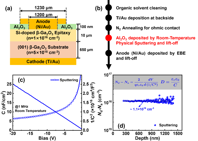
FIG. 1. (a) Schematic of the β-Ga₂O₃ SBD with Al₂O₃ field-plate termination, (b) fabrication flow, (c) C-V and 1/C2-V curves measured at 1 MHz and (d) calculated Nd-Na as a function of depth for the devices.
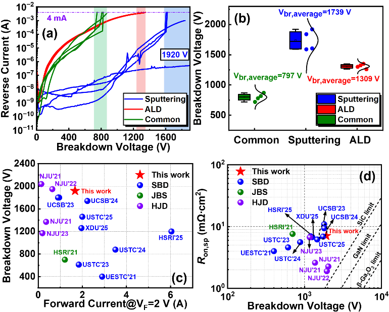
FIG. 2. (a) and (b) The breakdown characteristics of the devices. (c) and (d) The benchmark plots of representative state-of-the-art β-Ga₂O₃ with area about 1 mm².
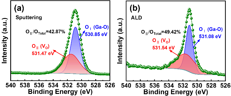
FIG. 3. XPS O 1s spectra of the Schottky interface with (a) Sputtering and (b) ALD FP-SBDs.
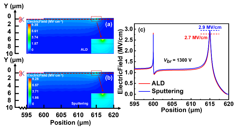
FIG. 4. Electric field contour plots of the (a) Sputtering and (b) ALD FP SBD, (c) simulated electric field profile for the two different SBDs for cutlines along the lateral direction.
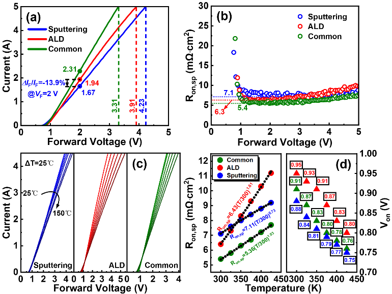
FIG. 5. (a) Linear-scale forward-bias I-V, (b) forward Ron,sp-V characteristics, (c) T-dependent forward I-V characteristics and (d) extracted dependence of Von and Ron,sp on Temperature.
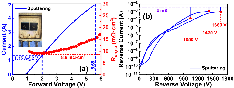
FIG. 6. (a) Linear-Scale forward I-V and Ron,sp-V characteristics with size of 1.2 mm in diameter. Inset of (a): photo of the packaged SBD in the TO-254 package. (b) The breakdown characteristics of packaged SBD at room temperature.
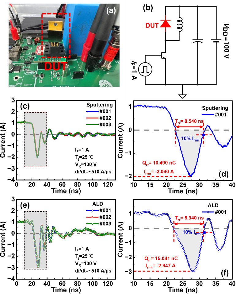
FIG. 7. Double-pulse test (DPT) characterization of the β-Ga₂O₃ SBD: (a) photograph of the PCB-based experimental setup, (b) corresponding circuit schematic. Measured reverse recovery waveforms for Sputtering and ALD devices: (c) and (e) show the full waveforms, while (d) and (f) provide magnified views of the transient recovery phases highlighted in (c) and (e).
DOI:
doi.org/10.1109/TED.2026.3714360
Instruction
Official Account

Cooperation
Top
