


Researchers from the Sun Yat-sen University have published a dissertation titled "Photonic-Electronic Dual-Passivated Ultrafast β-Ga₂O₃ SBUV Photodiode" in Small.
Background
Solar-blind ultraviolet (SBUV) photodetectors with ultrafast response are urgently required for aircraft exhaust plume monitoring, equipment fault early warning and other critical applications. Traditional infrared detection technology is severely disturbed by background noise such as solar radiation and complex thermal sources, leading to high false alarm rates. In contrast, ultraviolet light ranging from 200 to 280 nm is almost completely absorbed by atmospheric ozone, so natural SBUV background signal on the ground is extremely weak. Benefiting from this intrinsic characteristic, SBUV photodetection possesses outstanding anti-interference capability and low false-alarm probability, which makes it a core component for high-speed optoelectronic imaging and ultraviolet early-warning systems.
Nevertheless, mainstream β-Ga₂O₃-based SBUV photodetectors face a critical bottleneck of insufficient response speed. The photoresponse speed is jointly limited by RC time constant, carrier drift transport, slow carrier diffusion in non-depleted regions, and repeated trapping-detrapping dynamics at surface defect states. Photogenerated carriers produced outside the space-charge region diffuse sluggishly driven by concentration gradients, and surface dangling bonds/vacancies trap carriers which are gradually released to form long decay tails. These two slow carrier transport pathways severely prolong rise and decay time, making conventional devices incapable of capturing rapidly varying transient optical signals and hindering the practical deployment of high-speed imaging and real-time warning systems.
Existing single-passivation strategies can only suppress either delayed diffusion current or surface trap states separately, failing to eliminate both slow-response limiting factors simultaneously. Besides, most high-performance SBUV photodetectors require external bias voltage to operate, which raises system power consumption and circuit complexity. To address these challenges, this work proposes an integrated photonic-electronic dual-passivation (PEDP) device design strategy, achieves ultrafast photoresponse under zero bias based on vertical Schottky barrier photodiode architecture, and further fabricates an 8×8 pixel array to verify its high-speed imaging potential.
Abstract
Ultrafast response is a necessary characteristic for solar-blind ultraviolet (SBUV) photodetectors (PDs) in fault warning and aircraft exhaust plume monitoring. Here, for β-Ga₂O₃-based SBUV PDs, we propose a novel photonic-electronic dual-passivation (PEDP) strategy, which simultaneously mitigates carrier diffusion in non-depleted regions and surface trapping-detrapping dynamics. Consequently, the PEDP-modified PD achieves an ultrafast rise time of 5.9 ns and decay time of 86.8 ns at 0 V bias, outperforming existing SBUV PDs by 2-9 orders of magnitude. It also exhibits excellent overall performance at 0 V, including a dark current of 0.58 pA, photo-to-dark current ratio of 5.04 ×10⁴, rejection ratio (R₂₀₀ ₙₘ / R₃₅₀ ₙₘ) of 1.12 ×10⁴, responsivity of 0.084 A W⁻¹, and external quantum efficiency of 59.9%. These results demonstrate the feasibility of the PEDP strategy for fast-response SBUV detection and provide valuable insights for the development of fast imaging technologies.
Highlights
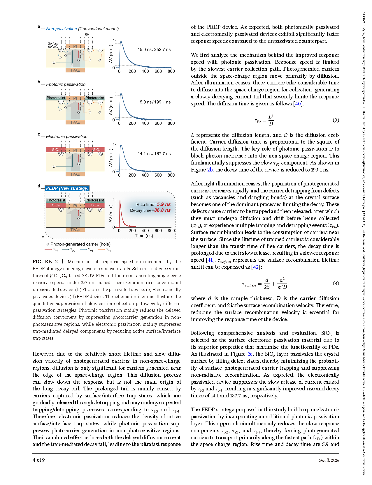
A novel photonic-electronic dual-passivation (PEDP) synergistic optimization strategy is proposed for the first time: amorphous SiO₂ electronic passivation layer fills surface defects to suppress carrier trapping and repeated detrapping; photoresist photonic passivation blocks SBUV light incidence in non-photosensitive zones, fundamentally eliminating slow diffusive carriers and simultaneously addressing two core loss mechanisms limiting response speed.
Vertical Pt/β-Ga₂O₃/Ti/Au Schottky barrier photodiode fabricated on β-Ga₂O₃ single crystal achieves nanosecond-level ultrafast response under zero bias, with rise time of 5.9 ns and decay time of 86.8 ns. Its zero-bias response speed surpasses all previously reported SBUV devices by 2-9 orders of magnitude, representing state-of-the-art performance among zero-biased β-Ga₂O₃ photodetectors.
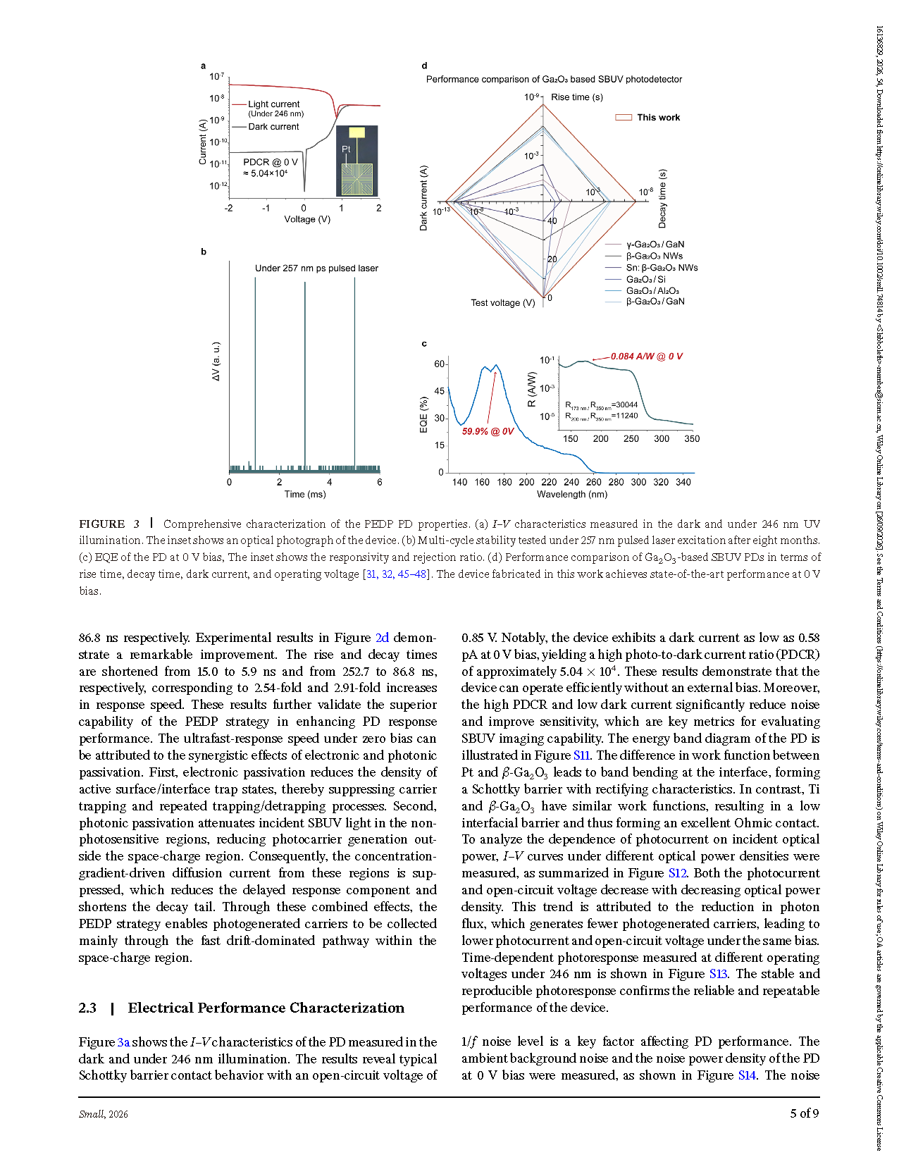
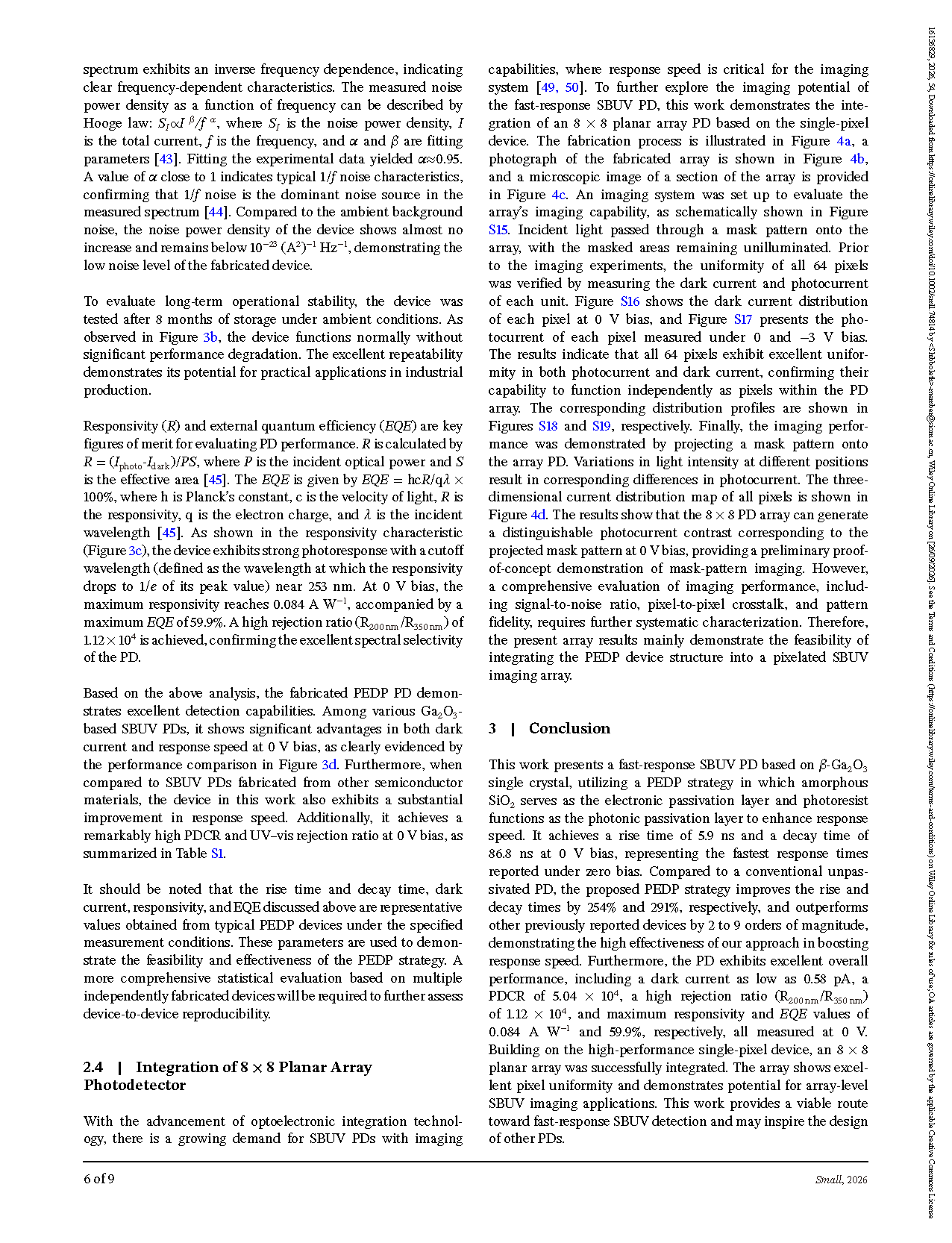
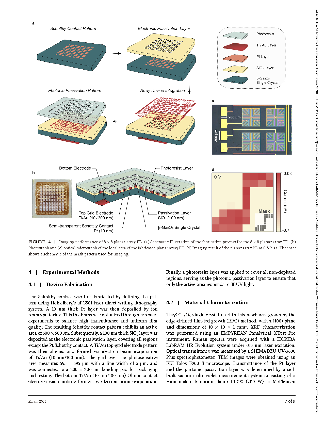
The device delivers balanced and outstanding comprehensive performance at 0 V bias, including ultra-low dark current (0.58 pA), high photo-to-dark current ratio (5.04×10⁴) and superior UV-visible rejection ratio (1.12×10⁴) with low noise and strong spectral selectivity. An 8×8 common-cathode pixel array is successfully integrated with excellent pixel uniformity, verifying the on-chip integration capability of the proposed structure for high-speed SBUV imaging chips.
Conclusion
This work presents a fast-response SBUV PD based on β-Ga₂O₃ single crystal, utilizing a PEDP strategy in which amorphous SiO₂ serves as the electronic passivation layer and photoresist functions as the photonic passivation layer to enhance response speed. It achieves a rise time of 5.9 ns and a decay time of 86.8 ns at 0 V bias, representing the fastest response times reported under zero bias. Compared to a conventional unpassivated PD, the proposed PEDP strategy improves the rise and decay times by 254% and 291%, respectively, and outperforms other previously reported devices by 2 to 9 orders of magnitude, demonstrating the high effectiveness of our approach in boosting response speed. Furthermore, the PD exhibits excellent overall performance, including a dark current as low as 0.58 pA, a photo-to-dark current ratio of 5.04 ×10⁴, a high rejection ratio (R₂₀₀ ₙₘ / R₃₅₀ ₙₘ) of 1.12 ×10⁴, and maximum responsivity and EQE values of 0.084 A W⁻¹ and 59.9%, respectively, all measured at 0 V. Building on the high-performance single-pixel device, an 8×8 planar array was successfully integrated. The array shows excellent pixel uniformity and demonstrates potential for array-level SBUV imaging applications. This work provides a viable route toward fast-response SBUV detection and may inspire the design of other PDs.
Project Support
This work was supported by the Natural Science Foundation of China (No. 62374186).
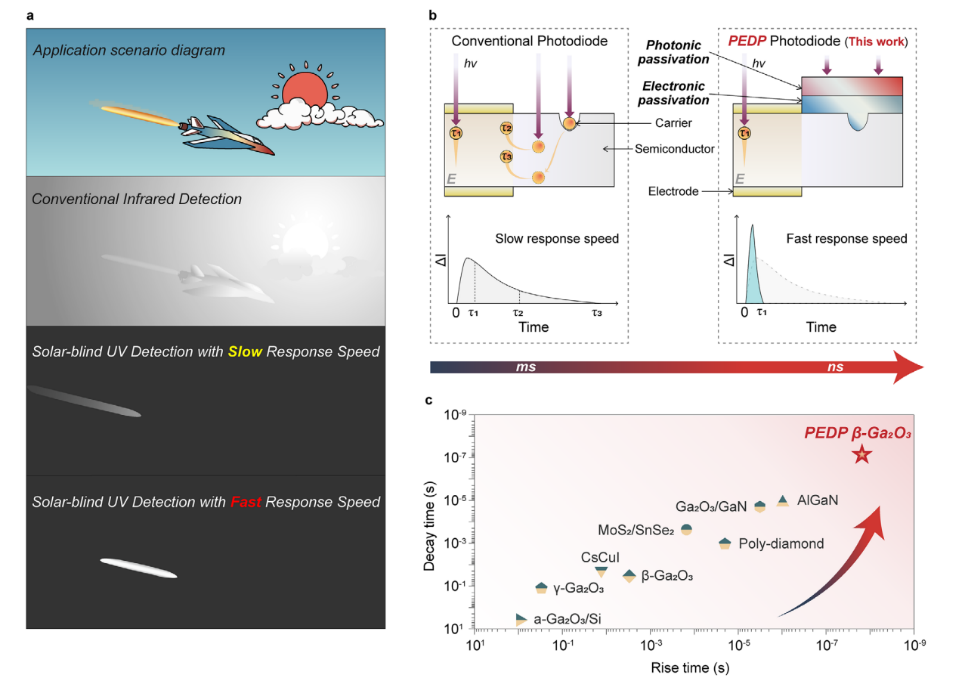
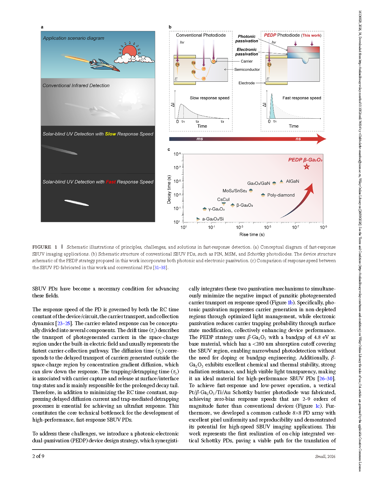
Figure 1 Schematic illustrations of principles, challenges, and solutions in fast-response detection. (a) Conceptual diagram of fast-response SBUV imaging applications. (b) Schematic structure of conventional SBUV PDs, such as PIN, MSM, and Schottky photodiodes. The device structure schematic of the PEDP strategy proposed in this work incorporates both photonic and electronic passivation. (c) Comparison of response speed between the SBUV PD fabricated in this work and conventional PDs
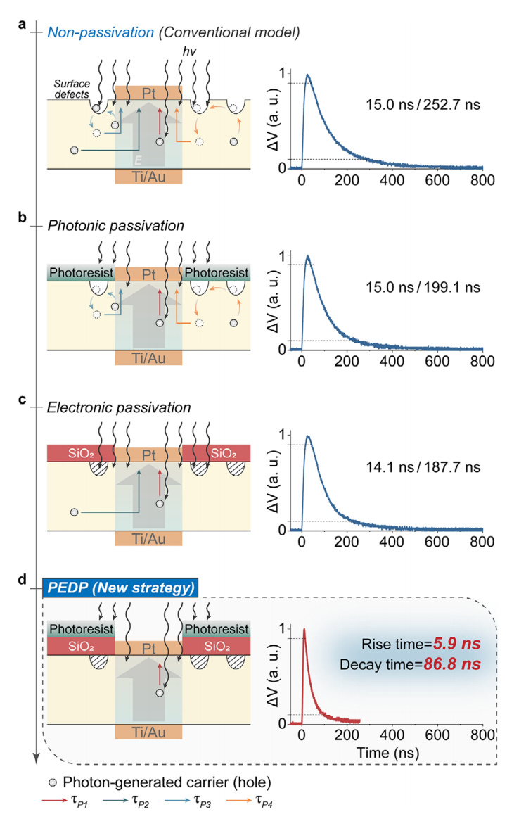
Figure 2 Mechanism of response speed enhancement by the PEDP strategy and single-cycle response results. Schematic device structure β-Ga₂O₃-based SBUV PDs and their corresponding single-cycle response speeds under 257 nm pulsed laser excitation: (a) Conventional unpassivated device. (b) Photonically passivated device. (c) Electronically passivated device. (d) PEDP device. The schematic diagrams illustrate the qualitative suppression of slow carrier-collection pathways by different passivation strategies. Photonic passivation mainly reduces the delayed diffusion component by suppressing photocarrier generation in nonphotosensitive regions, while electronic passivation mainly suppresses trap states
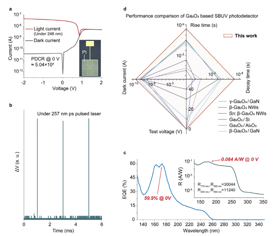
Figure 3 Comprehensive characterization of the PEDP PD properties. (a) I-V characteristics measured in the dark and under 246 nm UV illumination. The inset shows an optical photograph of the device. (b) Multi-cycle stability tested under 257 nm pulsed laser excitation after eight months. (c) EQE of the PD at 0 V bias, The inset shows the responsivity and rejection ratio. (d) Performance comparison of Ga₂O₃ based SBUV photodetector in terms of rise time, decay time, dark current, and operating voltage
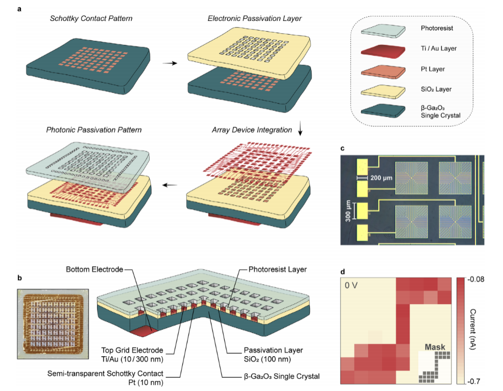
Figure 4 Imaging performance of 8×8 planar array PD. (a) Schematic illustration of the fabrication process for the 8×8 planar array PD. (b) Photograph and (c) optical micrograph of the local area of the fabricated planar array PD. (d) Imaging result of the planar array PD at 0 V bias. The inset shows a schematic of the mask pattern used for imaging
DOI:
doi.org/10.1002/smll.74814
Instruction
Official Account

Cooperation
Top
