


Recently, new progress has been achieved in device validation based on Ga₂O₃ substrates and epitaxial wafers supplied by Suzhou GAO Semiconductor Co., Ltd.
The research team fabricated vertical Schottky barrier diodes (SBDs) with field-plate-assisted mesa termination on (001) β-Ga₂O₃, achieving a breakdown voltage of 1,950 V.
The results, entitled “Enhanced Performance and Reliability in Ga₂O₃ Schottky Barrier Diodes with Field Plate Assisted Mesa Termination,” have been accepted for publication in Chinese Physics B.
From Material Characterization to Device Validation
For β-Ga₂O₃ materials intended for power electronics applications, conventional characterization techniques such as X-ray diffraction (XRD), surface morphology analysis, and carrier concentration measurements can provide insights into the fundamental quality of the material. However, whether the material can truly support high-voltage device applications ultimately needs to be verified through device fabrication and electrical testing.
In this work, (001) β-Ga₂O₃ substrates and epitaxial wafers supplied by Suzhou GAO Semiconductor Co., Ltd. were used to complete the fabrication and testing of vertical power devices, establishing a process pathway from material to device. The materials were successfully integrated with processes including mesa etching, SiO₂ dielectric deposition, Schottky and ohmic contact fabrication, and rapid thermal annealing (RTA), demonstrating good material quality and compatibility with device fabrication processes.
Achieving a Breakdown Voltage of 1,950 V
To further validate the capability of the material to support high-voltage devices, the research team fabricated both a reference device without edge termination and a field-plate-assisted mesa-termination device using the same material. The device without edge termination suffered from electric-field crowding at the anode edge and underwent premature breakdown at approximately 377 V. After introducing the field-plate-assisted mesa termination, the electric field at the device edge was effectively controlled, increasing the breakdown voltage to 1,950 V—an improvement of more than fivefold.
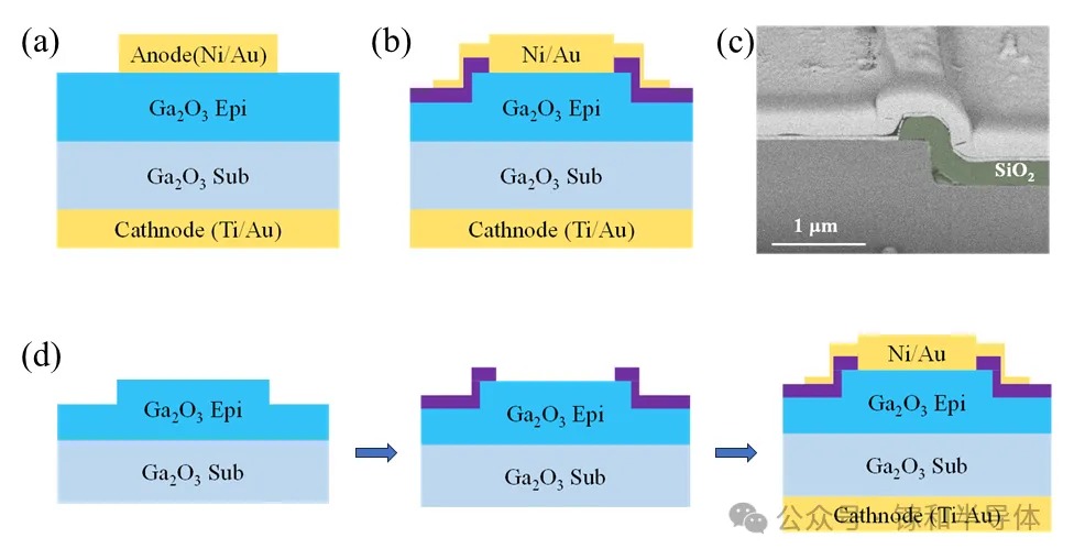
Figure 1. (a) Schematic structure of the reference Schottky barrier diode (REF-SBD) and (b) the field-plate-modulated Schottky barrier diode (FPM-SBD); (c) scanning electron microscopy (SEM) image of the FPM-SBD; and (d) fabrication process flow of the FPM-SBD.
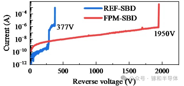
Figure 2. Reverse breakdown characteristics of the devices.
Meanwhile, the devices achieved a specific on-resistance of 7.9 mΩ·cm² and a turn-on voltage of approximately 0.90 V. At a forward bias of 2 V, the current density exceeded 80 A/cm², corresponding to a Baliga figure of merit of approximately 0.48 GW/cm², demonstrating a good balance between high breakdown voltage and low conduction loss.
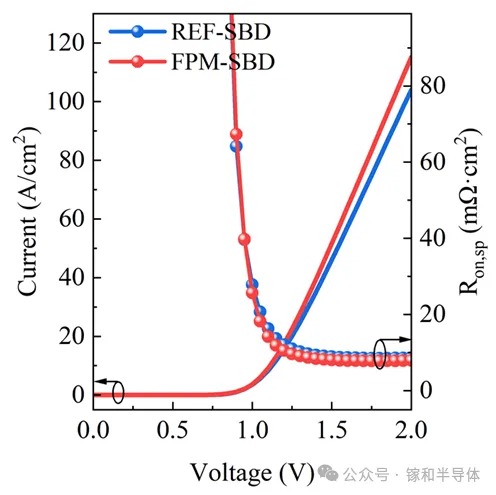
Figure 3. Forward conduction characteristics of the devices.
These results demonstrate that the (001) β-Ga₂O₃ material provided by Suzhou Gallium and Semiconductor exhibits good material quality and compatibility with device fabrication processes. With a properly designed device termination structure, its performance potential can be further exploited, enabling the device to achieve nearly 2 kV reverse blocking capability and demonstrating its potential for application in kilovolt-class vertical power devices.
High-Temperature Performance and Operational Stability Validated
Beyond the static characteristics at room temperature, the study also investigated the temperature dependence and bias stability of the devices. Over the temperature range of 25–200 °C, the devices maintained good rectification characteristics and a relatively stable forward voltage drop. After a 2.5 V forward-bias stress for 15 ks, the on-resistance changed by approximately 1.5%, demonstrating good operational stability.
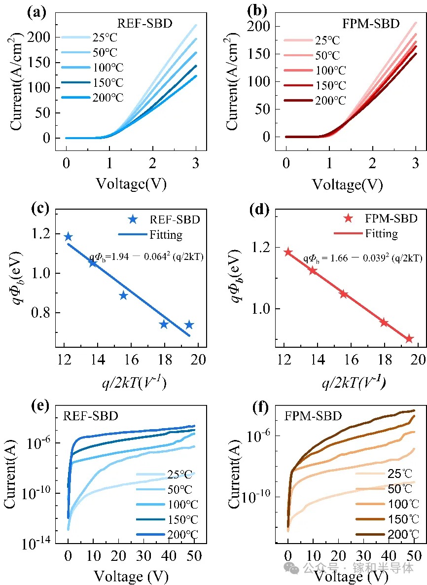
Figure 4. Temperature-dependent electrical characteristics of the REF-SBD and FPM-SBD.
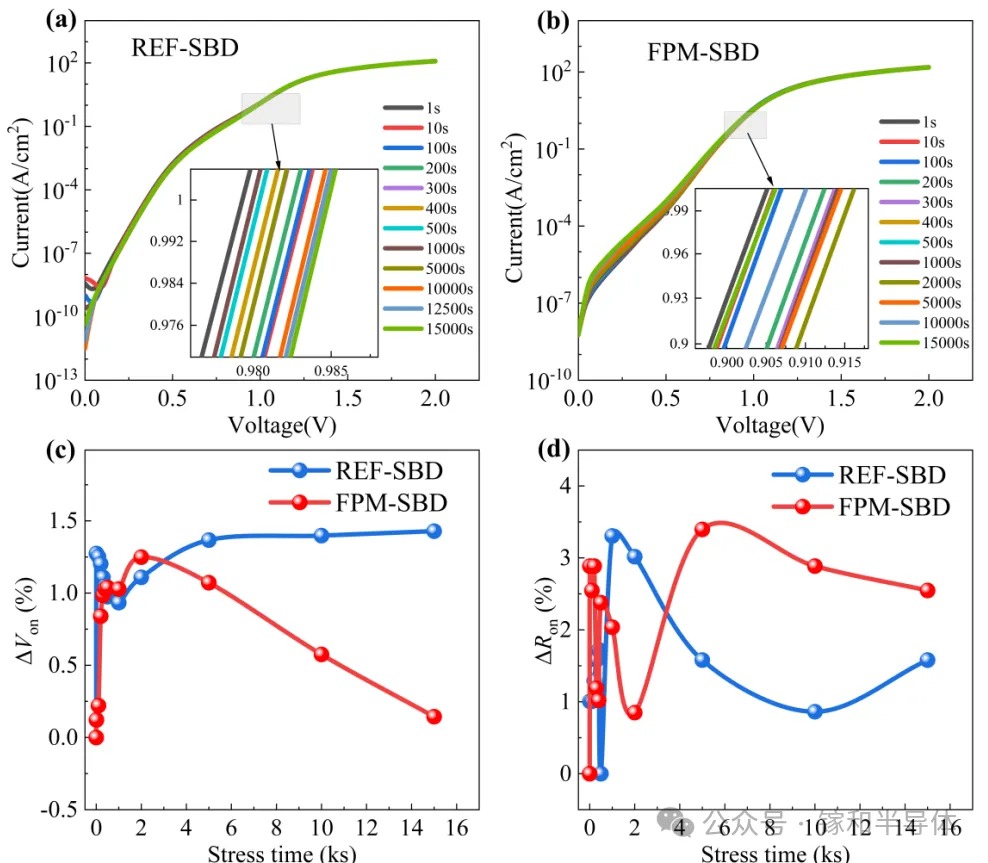
Figure 5. Stability testing of the REF-SBD and FPM-SBD under forward-bias stress, including the forward characteristics after different stress durations and the changes in turn-on voltage and on-resistance.
The successful realization of a near-2 kV vertical Schottky device comprehensively validates the quality, process compatibility, and high-voltage application capability of Gallium and Semiconductor’s (001) β-Ga₂O₃ material, further establishing an integrated validation chain spanning material preparation, device fabrication, and performance evaluation for gallium oxide.
Suzhou GAO Semiconductor:Products and Technical Capabilities

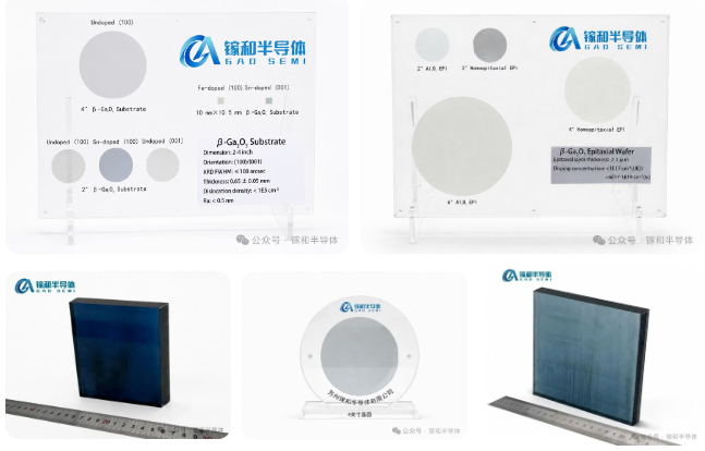
Suzhou GAO Semiconductor Co., Ltd. has long focused on β-Ga₂O₃ single-crystal growth, precision substrate processing, and epitaxial technology development. The company primarily adopts the edge-defined film-fed growth (EFG) method while also evaluating other growth approaches. It has established an integrated technical chain covering crystal growth, crystal orientation and electrical-property control, precision cutting, grinding and polishing, surface inspection, and epitaxial verification. This enables the company to provide single-crystal substrates, homoepitaxial/heteroepitaxial wafers, and customized material solutions for universities, research institutes, epitaxy companies, and device manufacturers.
At present, the company can stably supply 2–6-inch (100) and 2–4-inch (001) high-quality, twin-free Ga₂O₃ substrates, while 6-inch (001) Ga₂O₃ single-crystal samples have been successfully developed. Its product portfolio covers unintentionally doped, Fe-doped semi-insulating, and Sn-doped conductive substrates, with customization available according to crystal orientation, wafer size, epitaxial layer thickness, and doping requirements.
Rather than simply pursuing record wafer sizes, the company's technical focus is on continuously improving crystal integrity, electrical uniformity, surface quality, and batch-to-batch consistency as wafer dimensions are scaled up.
Instruction
Official Account

Cooperation
Top
