


Researchers from Guilin University of Electronic Technology have published a dissertation titled " Low-dimensional Ga₂O₃ nanostructures for optoelectronics: from dimensional engineering to device applications " in Journal of Alloys and Compounds.
Background
Gallium oxide (Ga₂O₃), as a representative ultrawide-bandgap semiconductor, has attracted increasing attention for applications in deep-ultraviolet detection, power electronics, transparent electronics, and emerging memory devices in recent years. Depending on its polymorph, crystal orientation, and optical-transition selection rules, Ga₂O₃ exhibits a theoretical breakdown electric field approaching 8 MV·cm⁻¹. In addition, Ga₂O₃ shows high chemical stability, thermal stability, and intrinsic deep ultraviolet absorption, which fundamentally originates from its ultrawide-bandgap spanning approximately 4.4 to 5.3 eV.
Abstract
Gallium oxide (Ga₂O₃), an ultrawide-bandgap semiconductor, has attracted considerable attention for solar-blind ultraviolet photodetection owing to its intrinsic deep-ultraviolet absorption, high breakdown field, and excellent chemical and thermal stability. However, conventional Ga₂O₃-based devices still face challenges associated with limited carrier modulation capability, defect-induced carrier trapping, and insufficient integration potential. Low-dimensional Ga₂O₃ nanostructures provide effective solutions by offering enhanced surface effects, shortened carrier transport pathways, and tunable electronic properties. This review summarizes recent advances in one-dimensional and two-dimensional Ga₂O₃ nanostructures, with particular emphasis on synthesis strategies, dimensional engineering, defect regulation, and optoelectronic device applications. Representative photodetector architectures, including metal-semiconductor-metal devices, Schottky junctions, heterostructures, and phototransistors, are discussed. The mechanisms underlying persistent photoconductivity and carrier dynamics are also discussed. Finally, current challenges are discussed, and future perspectives toward high-performance and integrated Ga₂O₃ optoelectronic systems are presented.
Conclusion
Looking forward, 2D Ga₂O₃ is expected to become an increasingly important platform for next-generation ultraviolet optoelectronics because its intrinsic low-dimensional characteristics provide functionalities that are difficult to achieve in conventional bulk materials. In particular, the low-symmetry monoclinic crystal structure of β-Ga₂O₃ gives rise to pronounced in-plane structural anisotropy, resulting in orientation dependent optical absorption, carrier transport, dielectric response, and effective mass. Unlike conventional polarization-sensitive photodetectors that rely on external polarizers or artificially patterned metasurfaces, intrinsic crystal anisotropy enables direct polarization discrimination at the material level. Specifically, preferential growth of one-dimensional Ga₂O₃ nanostructures along specific crystallographic directions, such as the [001] and [010] orientations, can effectively couple polarization direction with anisotropic carrier transport pathways, thereby amplifying polarization-dependent photocurrent. For two-dimensional Ga₂O₃ nanosheets, exposed crystal facets, including (100) and (001) planes, provide distinct surface atomic configurations and in-plane anisotropic electronic states, enabling facet-dependent polarization responses. When combined with the atomically thin geometry of 2D nanosheets, enhanced light–matter interaction, reduced dielectric screening, and strong interfacial tunability further enhance anisotropic photoresponse, making 2D Ga₂O₃ particularly suitable for compact polarization-sensitive solar-blind photodetectors. Future studies should therefore focus on crystallographic orientation engineering, anisotropic strain modulation, and heterostructure design to fully exploit the polarization-dependent electronic and optical properties of 2D Ga₂O₃. Beyond individual photodetectors, the future development of low-dimensional Ga₂O₃ is expected to move toward large-area integrated systems. One promising direction is the monolithic integration of 2D Ga₂O₃ with flexible substrates such as polyimide, mica, and ultrathin glass through low-temperature transfer printing or wafer-scale growth techniques. Combined with flexible transparent electrodes, van der Waals heterostructures, and mechanically robust encapsulation strategies, such devices could enable wearable solar-blind ultraviolet monitoring for environmental sensing, healthcare, flame detection, and space applications while maintaining excellent mechanical reliability under repeated bending conditions. Another important trend is the integration of Ga₂O₃ photodetectors with memristive and neuromorphic devices into in-sensor computing architectures. Benefiting from persistent photoconductivity, defect-mediated carrier dynamics, and compatibility with oxide electronic platforms, low-dimensional Ga₂O₃ offers opportunities for integrating sensing, memory, and computation within a single hardware platform. Large-scale photodetector arrays capable of polarization imaging, ultraviolet imaging, artificial visual perception, and edge intelligence may therefore represent an important future direction for Ga₂O₃-based optoelectronic systems.
Project Support
This work was supported by Guangxi Science and Technology Plan Project (AD24010060, XT2503960010, AD25069103), National Natural Science Foundation of China (No. 52262022, U25A20481, 62205080, 62361022), Innovation Project of GUET Graduate Education (2026YCXB005).
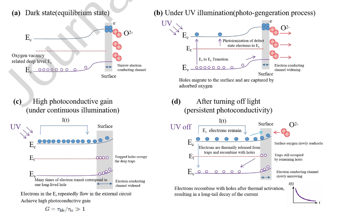
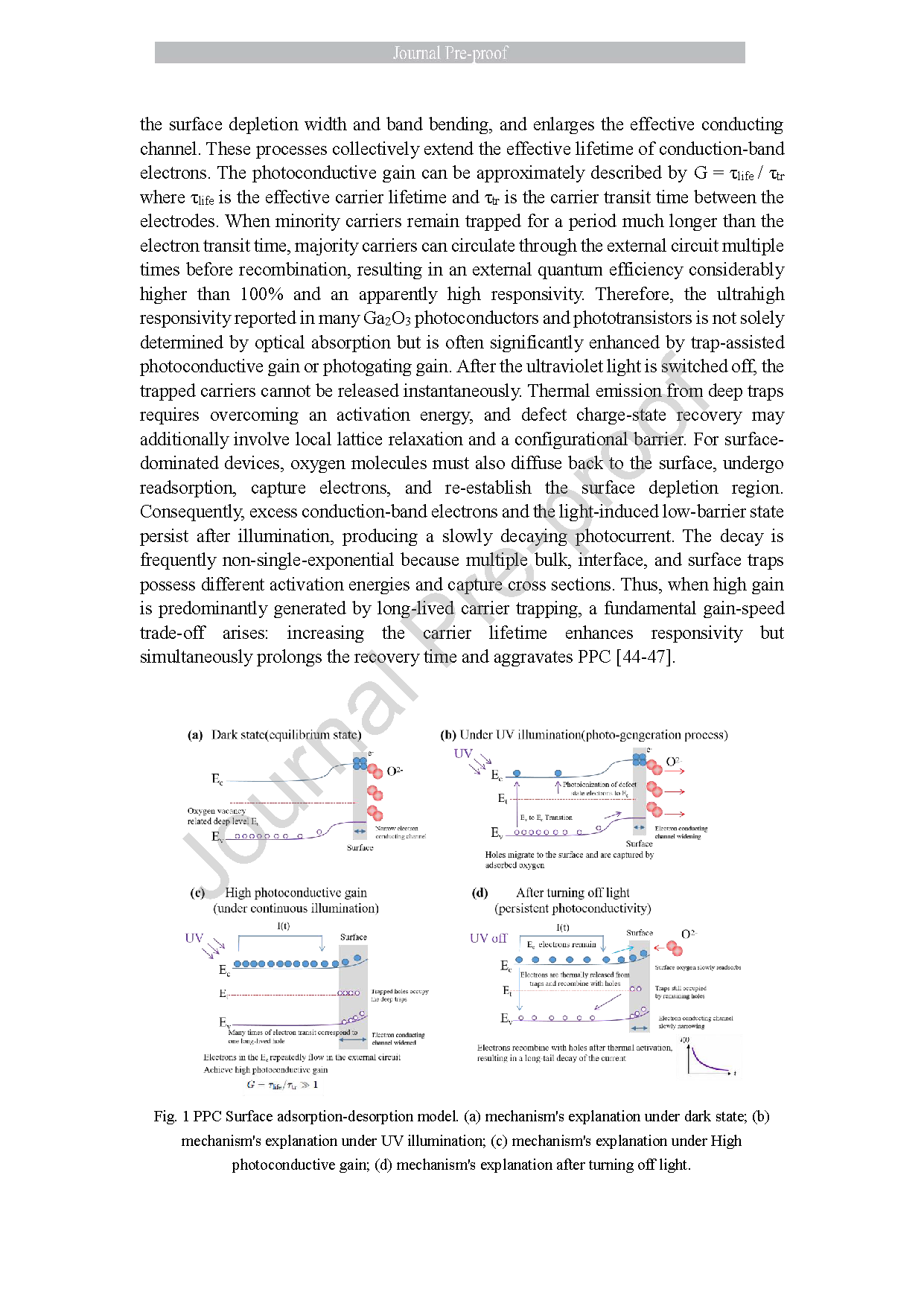
Fig. 1 PPC Surface adsorption-desorption model. (a) mechanism explanation under dark conditions; (b) mechanism explanation under UV illumination; (c) mechanism explanation under High photoconductive gain; (d) mechanism explanation after turning off light.

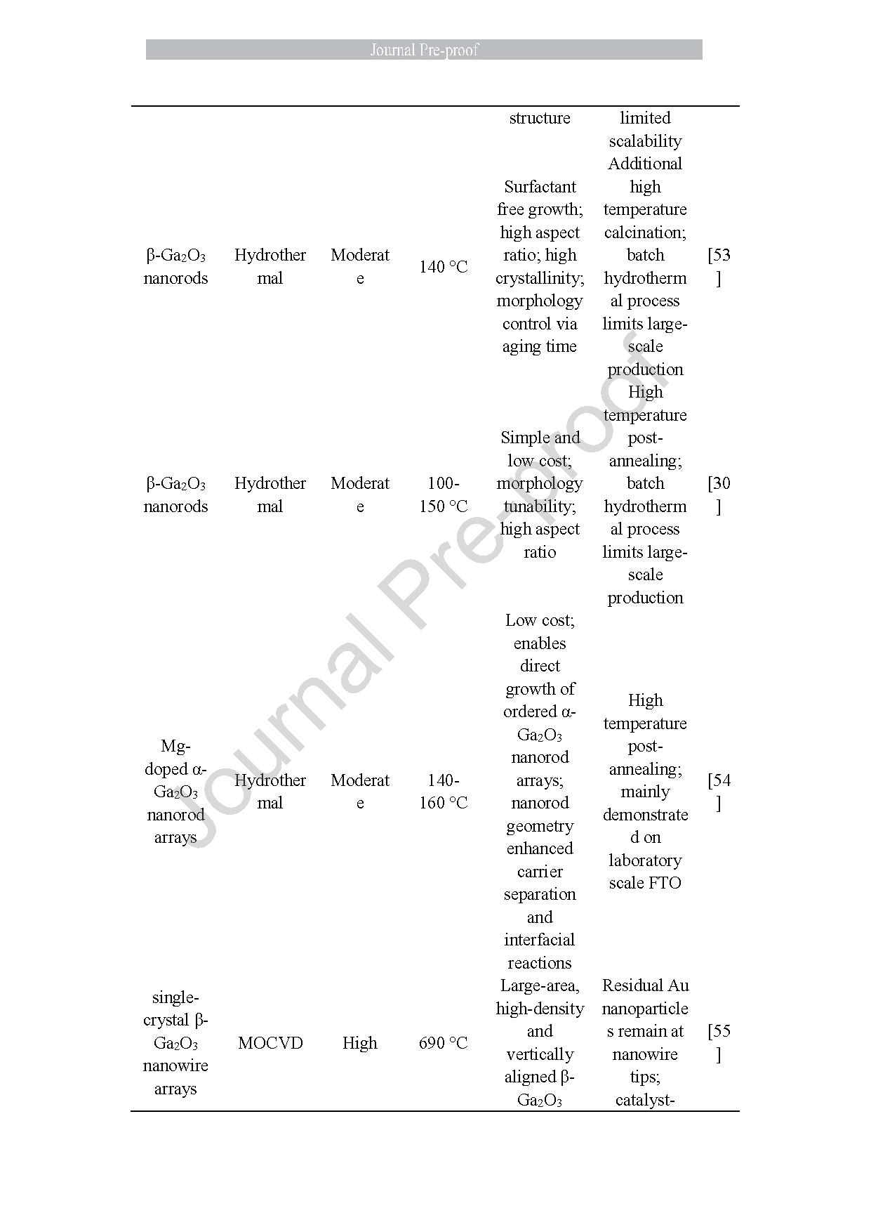
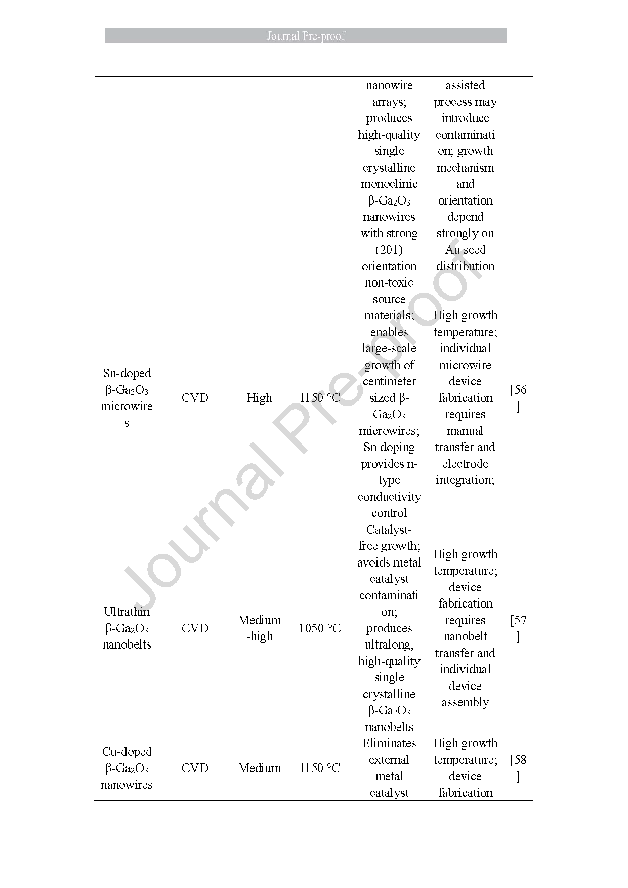
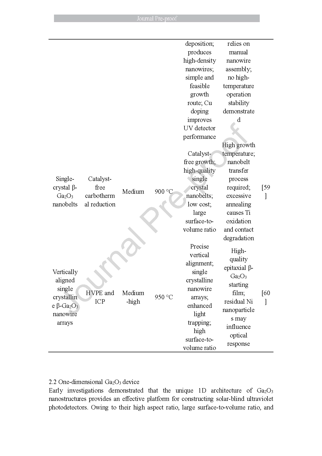
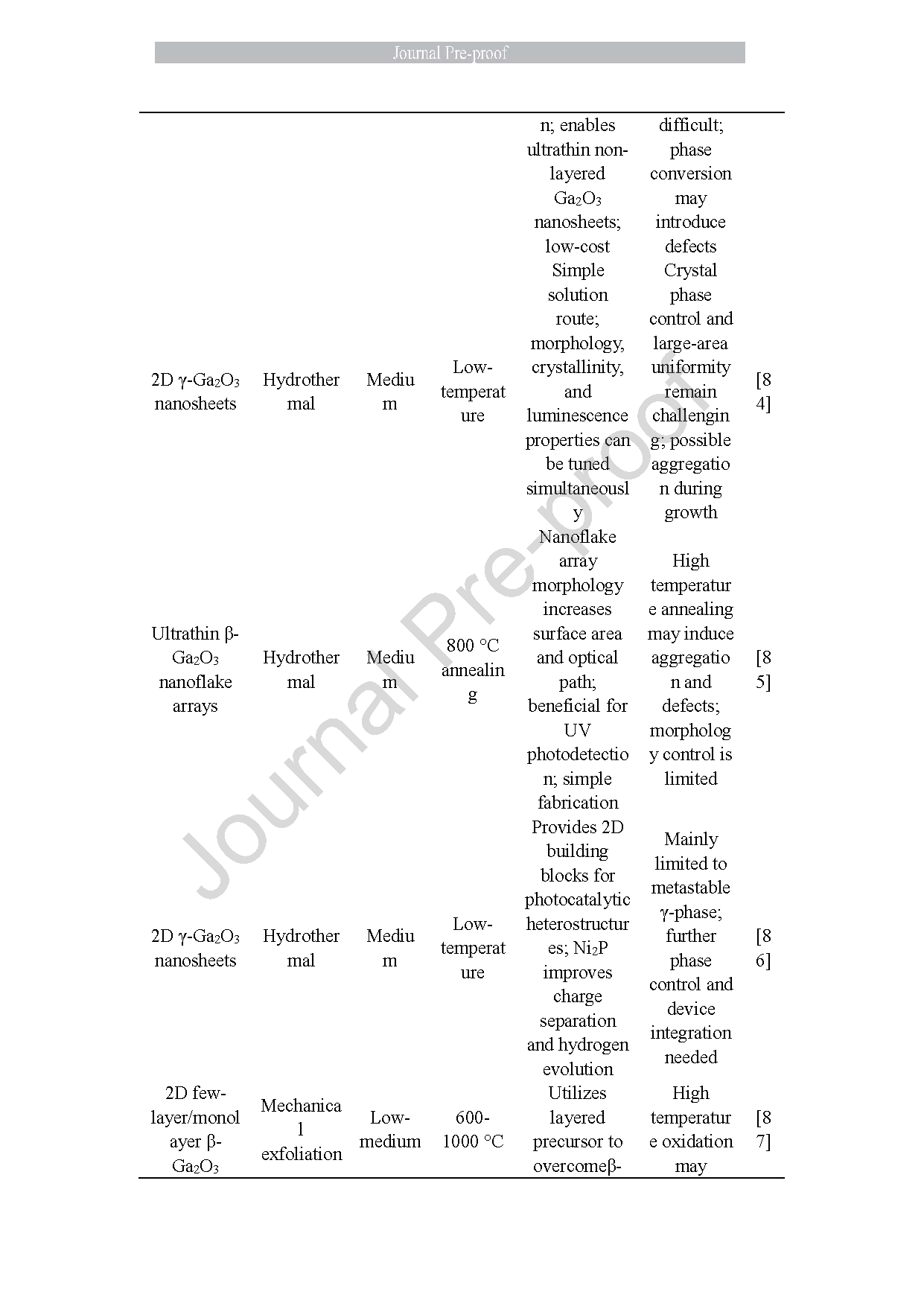
Fig. 2 Morphology image of 1D Ga₂O₃ nanostructures. (a, b) β-Ga₂O₃ nanostructures grown on Si; (c, d) β-Ga₂O₃ nanostructures grown on AlN/Si; (e, f) β-Ga₂O₃ nanostructures grown on ZnO/Si substrates; (g, h) α-Ga₂O₃ and Mg-Ga₂O₃ nanorods; (i) Sn-doped β-Ga₂O₃ microwire array; (j) single Sn-doped β-Ga₂O₃ microwires; (k) hundreds of Ga₂O₃ nanobelts; (l) one Ga₂O₃ nanobelt; (m) Cu:β-Ga₂O₃ nanowires: Low-magnification; (n) Cu: β-Ga₂O₃ nanowires: High-magnification; (o) β-Ga₂O₃ nanostructures synthesized by carbothermal reduction; (p) vertical β-Ga₂O₃ nanowire.
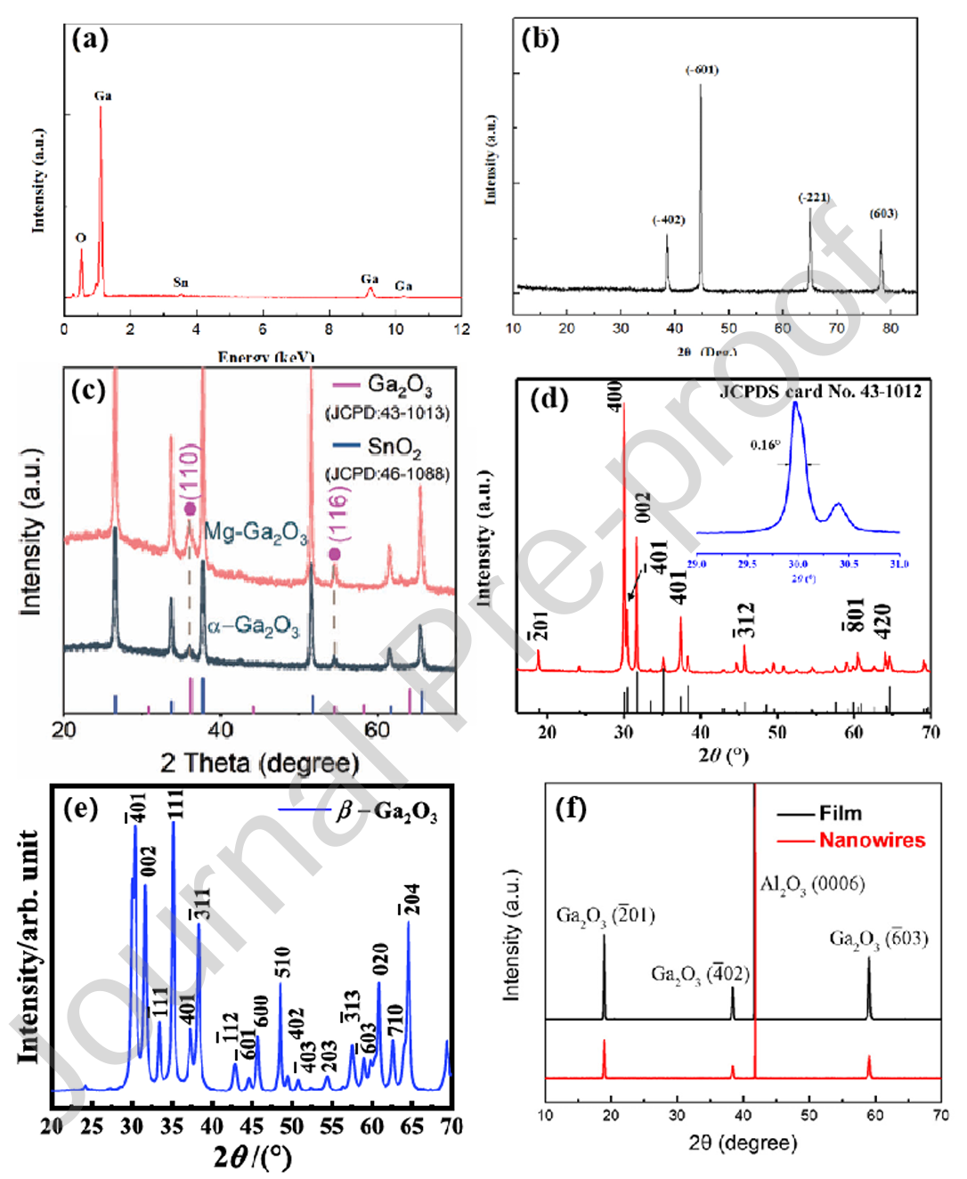
Fig. 3 Image of 1D Ga₂O₃ elemental composition and crystal orientation. (a) The EDS spectrum of single Sn-doped β-Ga₂O₃ microwire; (b) XRD pattern of single β-Ga₂O₃ microwire; (c) XRD pattern of α-Ga₂O₃ and Mg-Ga₂O₃; (d) XRD image of a 17.3 nm β-Ga₂O₃ nanobelt; (e) XRD pattern of β-Ga₂O₃ nanostructures synthesized by carbothermal reduction; (f) XRD patterns of single-crystalline β-Ga₂O₃ nanowire arrays.
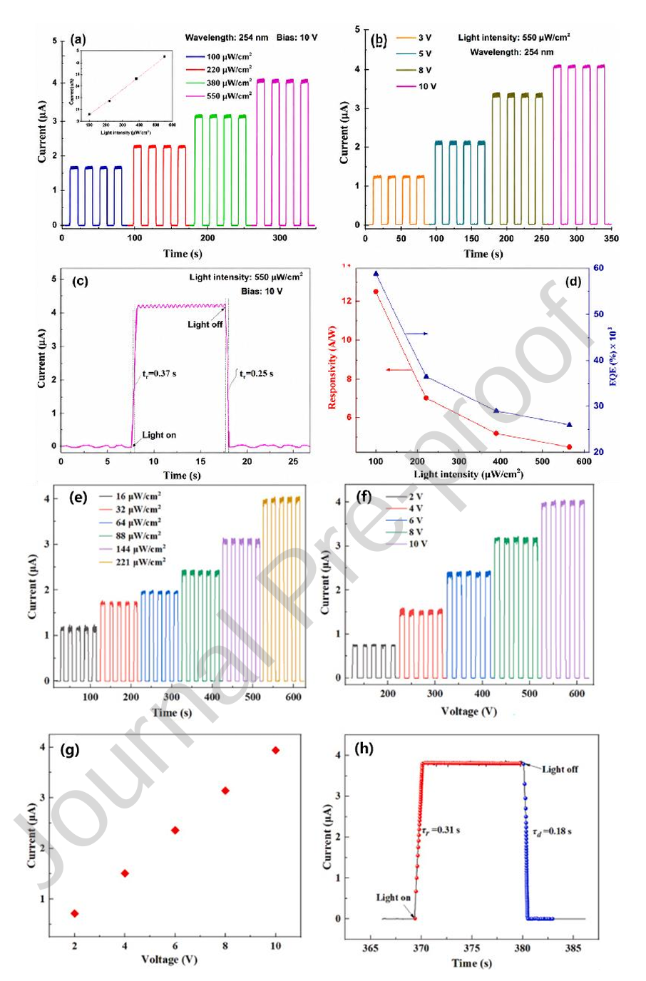
Fig. 4 Photoresponse behavior and performance parameters of MSM photodetectors. (a) time dependent photoresponse for photodetector based on a single Sn-doped β-Ga₂O₃ microwire under 254 nm light with different light intensities at 10 V; (b) time-dependent response of a single Sn doped β-Ga₂O₃ UV detector at different biases; (c) enlarged view of the rise/decay edges of single Sn-doped β-Ga₂O₃ microwire photodetector; (d) single Sn-doped β-Ga₂O₃ microwire photodetector’s responsivity of the light intensities at 10 V; (e) I-t curves of Cu: β-Ga₂O₃ nanowire photodetector under different light power densities at 10 V; (f) I-t curves of Cu: β-Ga₂O₃ nanowire photodetector at various voltages; (g) photocurrent dependence of Cu:β-Ga₂O₃ nanowire photodetector on the versus bias voltage; (h) time response curve of 254 nm Cu: β-Ga₂O₃ nanowire UV photodetector under a single 254 nm UV pulse irradiation.
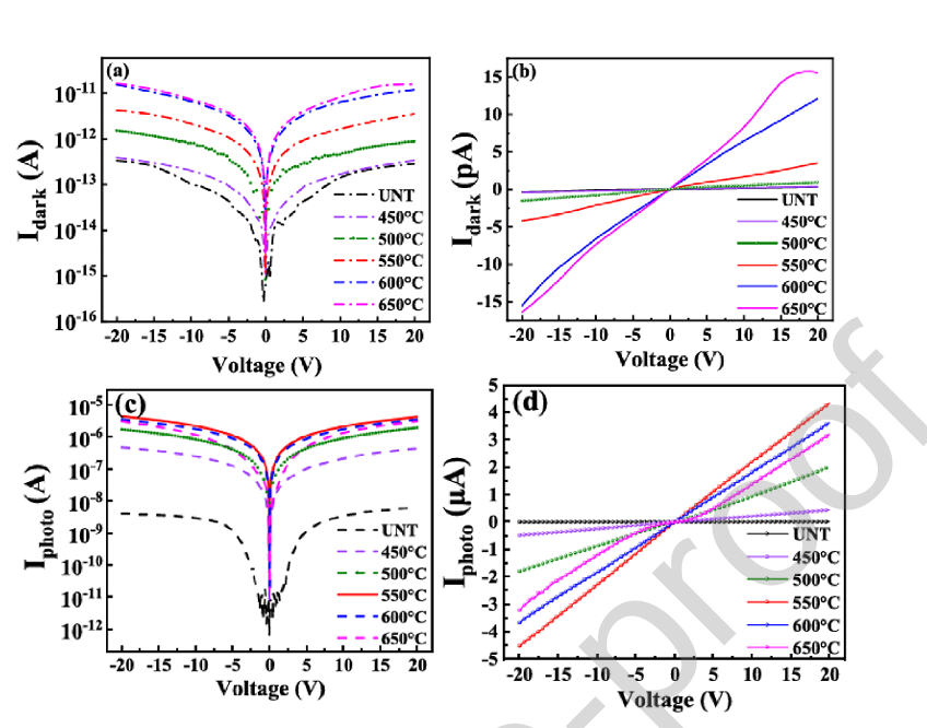
Fig. 5 Effect of annealing treatment on the dark and photocurrent characteristics of β-Ga₂O₃ nanobelt MSM solar-blind UV photodetectors. (a) Idark curves of β-Ga₂O₃ nanobelt MSM solar blind UV photodetectors at different annealing temperatures Ta in logarithmic coordinate; (b) Idark curves of β-Ga₂O₃ nanobelt MSM solar-blind UV photodetectors at different Ta in linear coordinate; (c, d) Iphoto curves of β-Ga₂O₃ nanobelt MSM solar-blind UV photodetectors at different Ta.
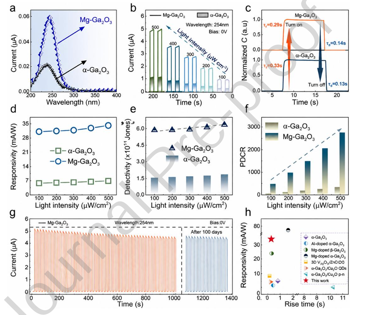
Fig. 6 Comprehensive photoelectrical performance of Mg-doped α-Ga₂O₃ self-powered solar-blind ultraviolet photodetectors. (a) Spectral response of α-Ga₂O₃ and Mg-doped Ga₂O₃; (b) Comparison of α-Ga₂O₃ and Mg-doped Ga₂O₃ I-T curves for two SBPDs at 0 V bias, 254 nm illumination, and varying light intensities; (c) α-Ga₂O₃ and Mg-doped Ga₂O₃ time response comparison of the two self-powered photodetectors (SBPDs); (d) α-Ga₂O₃ and Mg-doped Ga₂O₃ responsivity of the two SBPDs as a function of light power density; (e) α-Ga₂O₃ and Mg-doped Ga₂O₃ detectivity comparison of the two SBPDs; (f) α-Ga₂O₃ and Mg-Ga₂O₃ photo-dark current ratio under varying light power densities; (g) stability test curve for the Mg-doped Ga₂O₃ SBPD; (h) responsivity and time response of Mg-doped Ga₂O₃ SBPD in comparison with previously reported works.
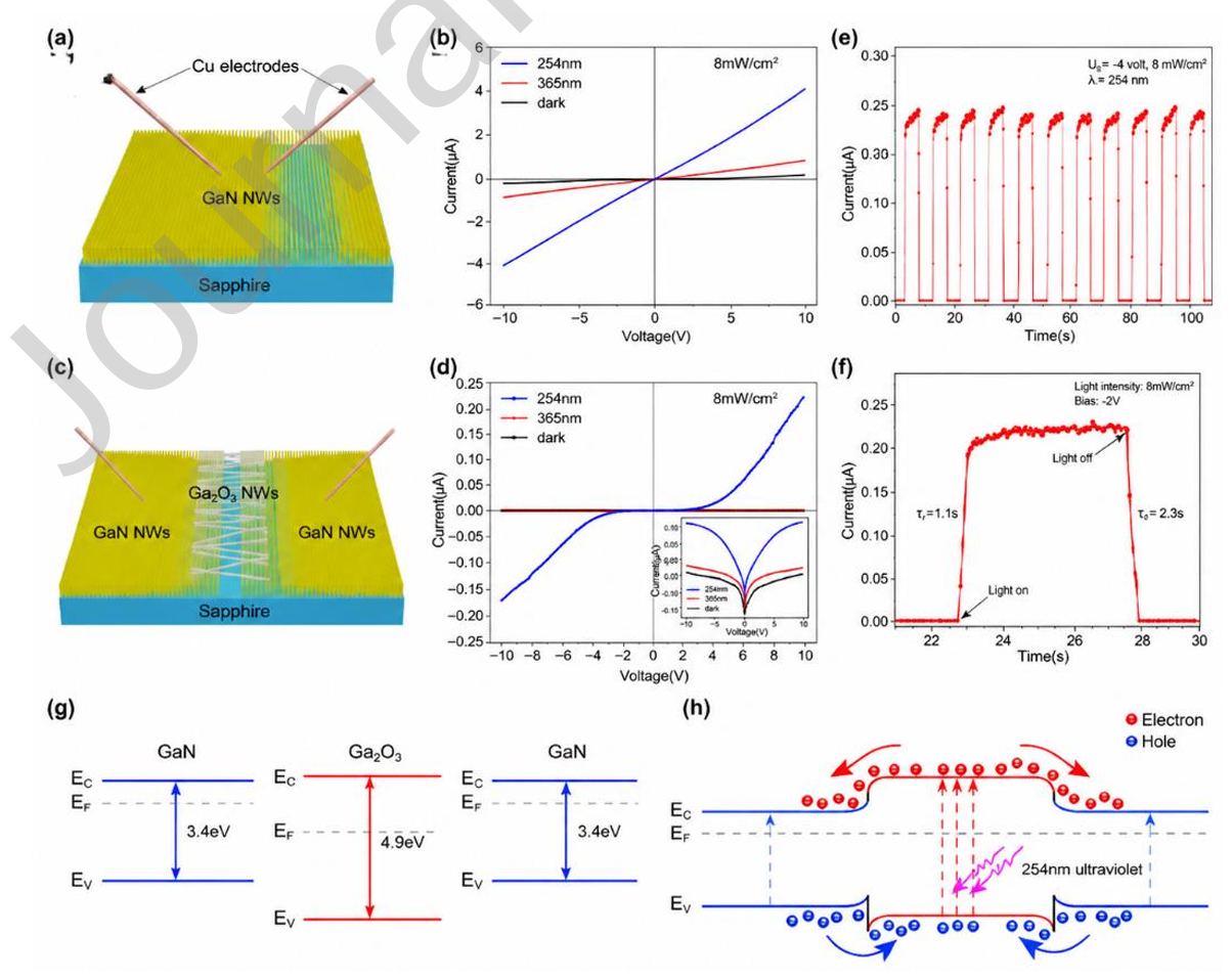
Fig. 7 Device structure, photoresponse characteristics, and carrier transport mechanism of β Ga₂O₃/GaN nanowire heterojunction solar-blind ultraviolet photodetectors. (a) schematic diagram of β-Ga₂O₃/GaN nanowire photodetectors; (b) I-V characteristics of the GaN nanowires; (c) schematic diagram of β-Ga₂O₃/GaN nanowire photodetectors; (d) I-V characteristics of the β Ga₂O₃/GaN nanowire UV detector; (e) photocurrent-time responses of the β-Ga₂O₃/GaN nanowire UV detector under 254 nm UV illumination at 10 V bias; (f) β-Ga₂O₃/GaN nanowire photocurrent time responses over one cycle; (g) schematic energy band diagrams before β-Ga₂O₃ contacts GaN; (h) β-Ga₂O₃/GaN nanowire schematic energy band diagrams at 0 V bias (after contact).
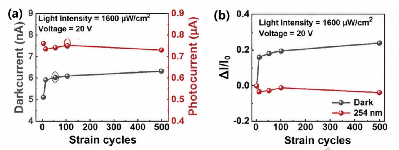
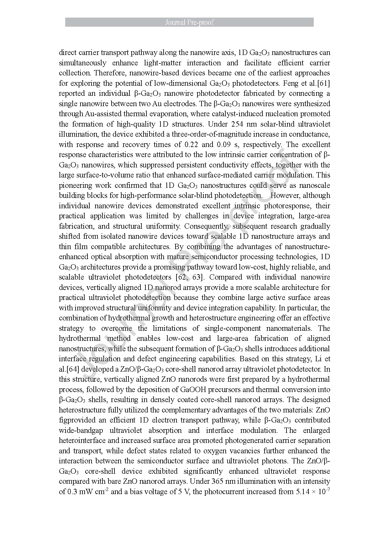
Fig. 8 Strain stability analysis of the stretchable UV-blind photodetector based on β-Ga₂O₃ nanowires. (a) β-Ga₂O₃ nanowires changes in photoelectric current and dark current of the device after 500 cycles of 0-50%-0% tensile strain; (b) β-Ga₂O₃ nanowires changes in photoelectric current and dark current rates of the device after 500 cycles of 0-50%-0% tensile strain.
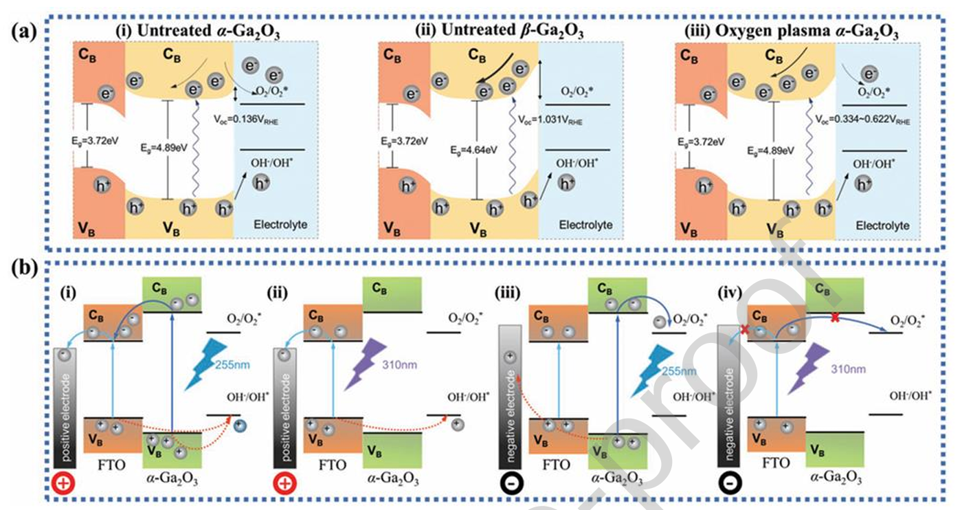
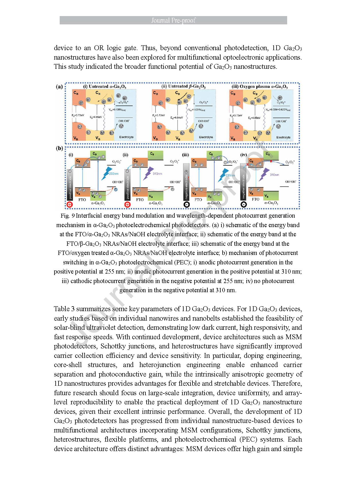
Fig. 9 Interfacial energy band modulation and wavelength-dependent photocurrent generation mechanism in α-Ga₂O₃ photoelectrochemical photodetectors. (a) i) schematic of the energy band at the FTO/α-Ga₂O₃ NRAs/NaOH electrolyte interface; ii) schematic of the energy band at the FTO/β-Ga₂O₃ NRAs/NaOH electrolyte interface; iii) schematic of the energy band at the FTO/oxygen treated α-Ga₂O₃ NRAs/NaOH electrolyte interface; b) mechanism of photocurrent switching in α-Ga₂O₃ photoelectrochemical (PEC); i) anodic photocurrent generation in the positive potential at 255 nm; ii) anodic photocurrent generation in the positive potential at 310 nm; iii) cathodic photocurrent generation in the negative potential at 255 nm; iv) no photocurrent generation in the negative potential at 310 nm.
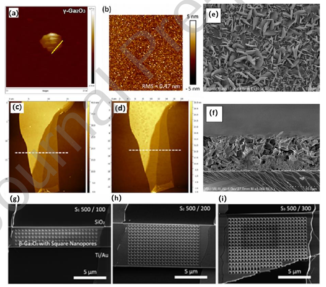
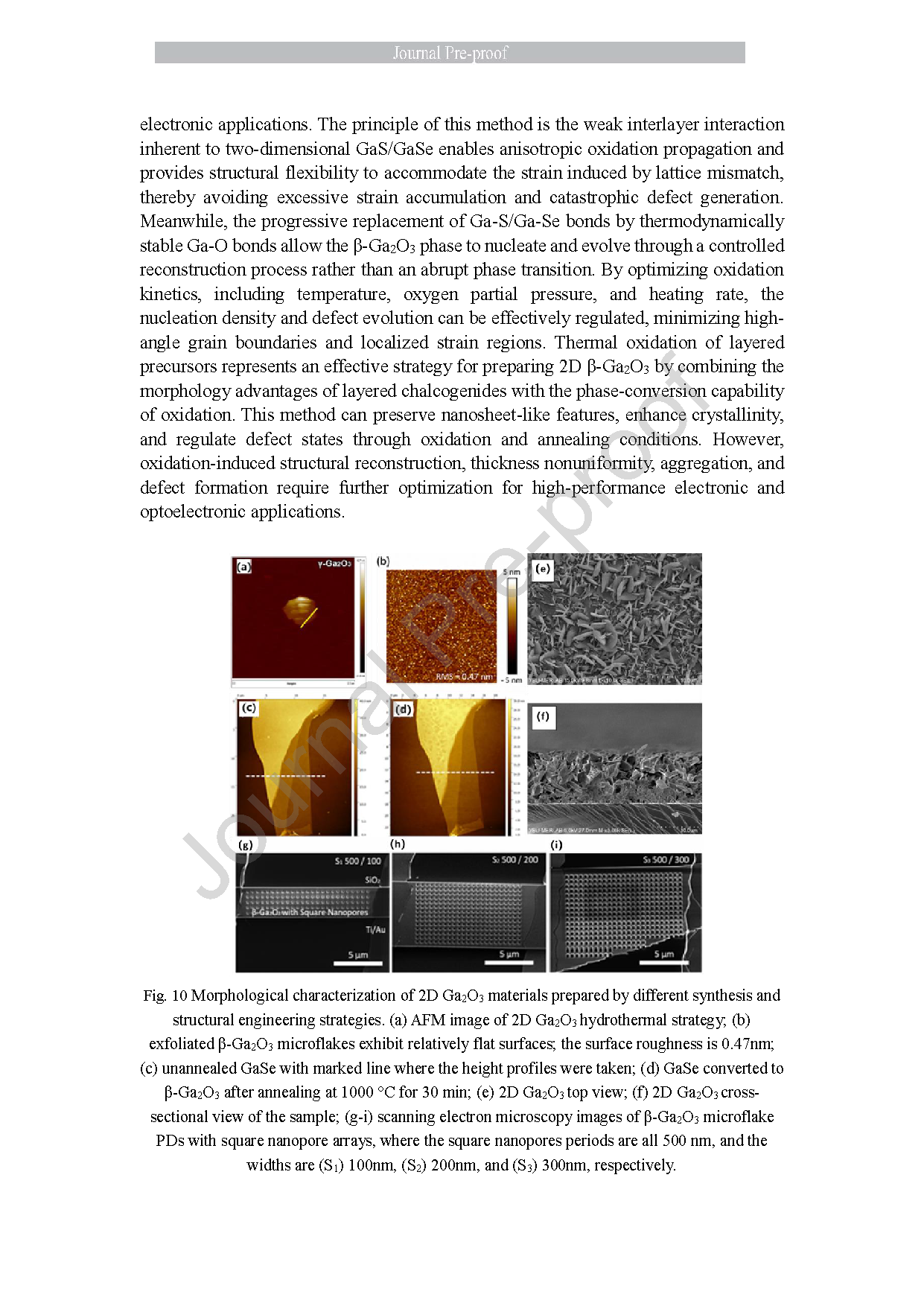
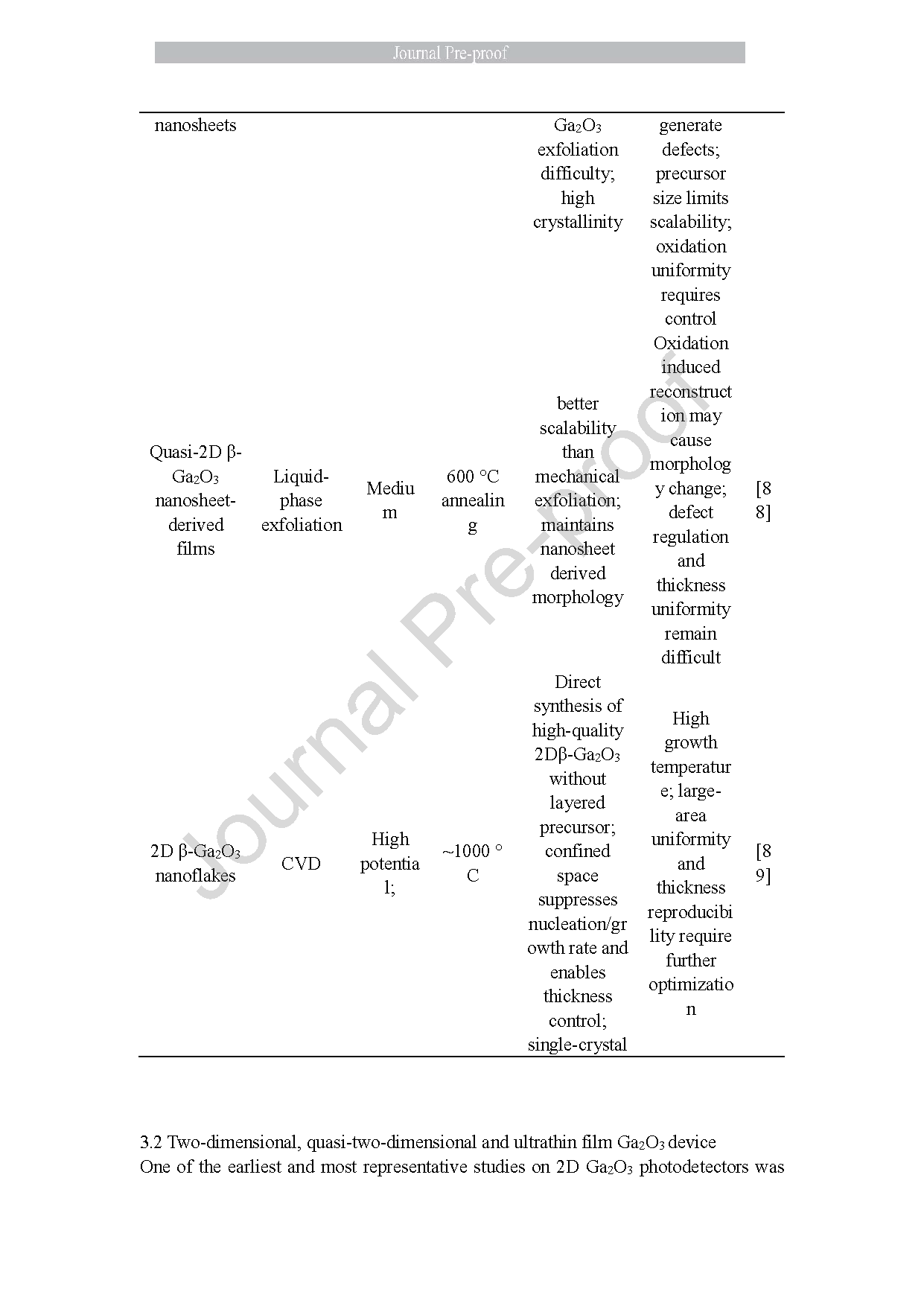
Fig. 10 Morphological characterization of 2D Ga₂O₃ materials prepared by different synthesis and structural engineering strategies. (a) AFM image of 2D Ga₂O₃ hydrothermal strategy; (b) exfoliated β-Ga₂O₃ microflakes exhibit relatively flat surfaces; the surface roughness is 0.47nm; (c) unannealed GaSe with marked line where the height profiles were taken; (d) GaSe converted to β-Ga₂O₃ after annealing at 1000 °C for 30 min; (e) 2D Ga₂O₃ top view; (f) 2D Ga₂O₃ cross sectional view of the sample; (g-i) scanning electron microscopy images of β-Ga₂O₃ microflake PDs with square nanopore arrays, where the square nanopores periods are all 500 nm, and the widths are (S1) 100nm, (S2) 200nm, and (S3) 300nm, respectively.
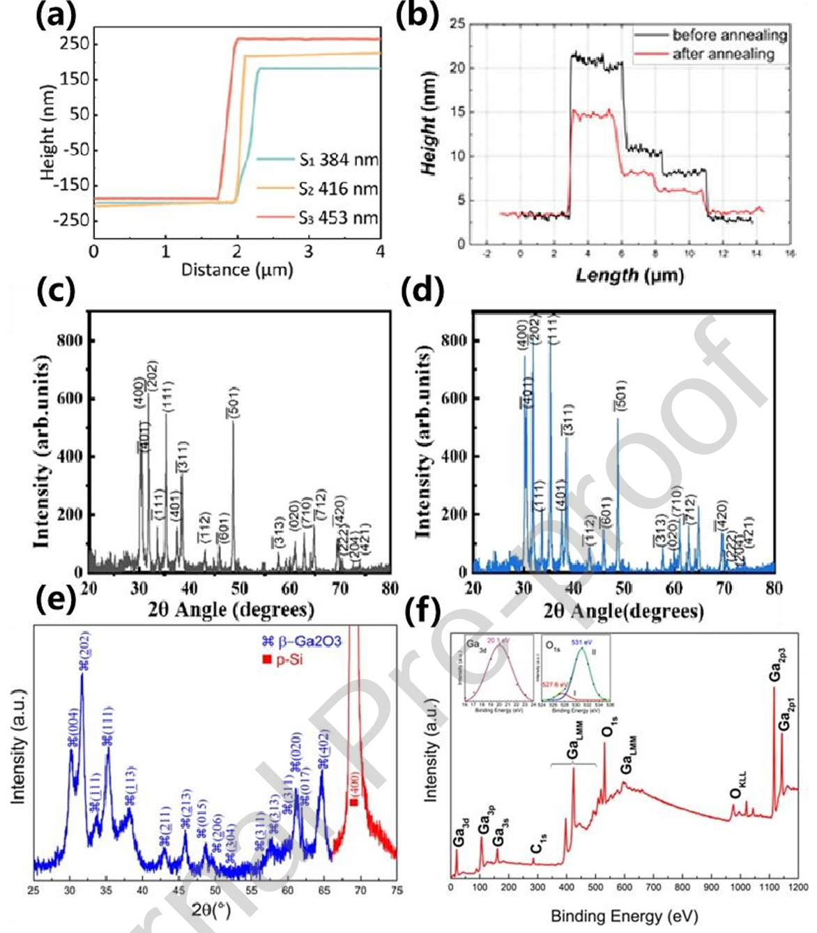
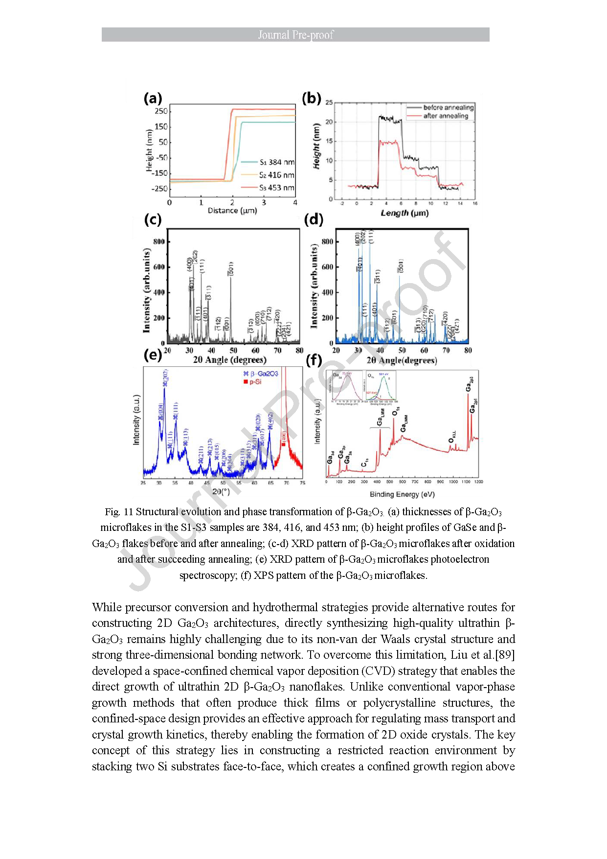
Fig. 11 Structural evolution and phase transformation of β-Ga₂O₃. (a) thicknesses of β-Ga₂O₃ microflakes in the S1-S3 samples are 384, 416, and 453 nm; (b) height profiles of GaSe and β Ga₂O₃ flakes before and after annealing; (c-d) XRD pattern of β-Ga₂O₃ microflakes after oxidation and after succeeding annealing; (e) XRD pattern of β-Ga₂O₃ microflakes photoelectron spectroscopy; (f) XPS pattern of the β-Ga₂O₃ microflakes.
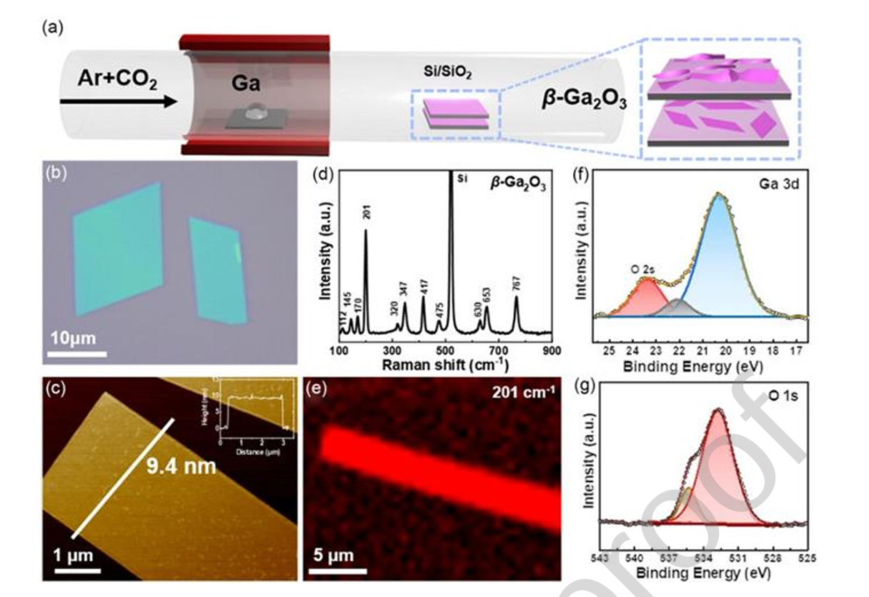
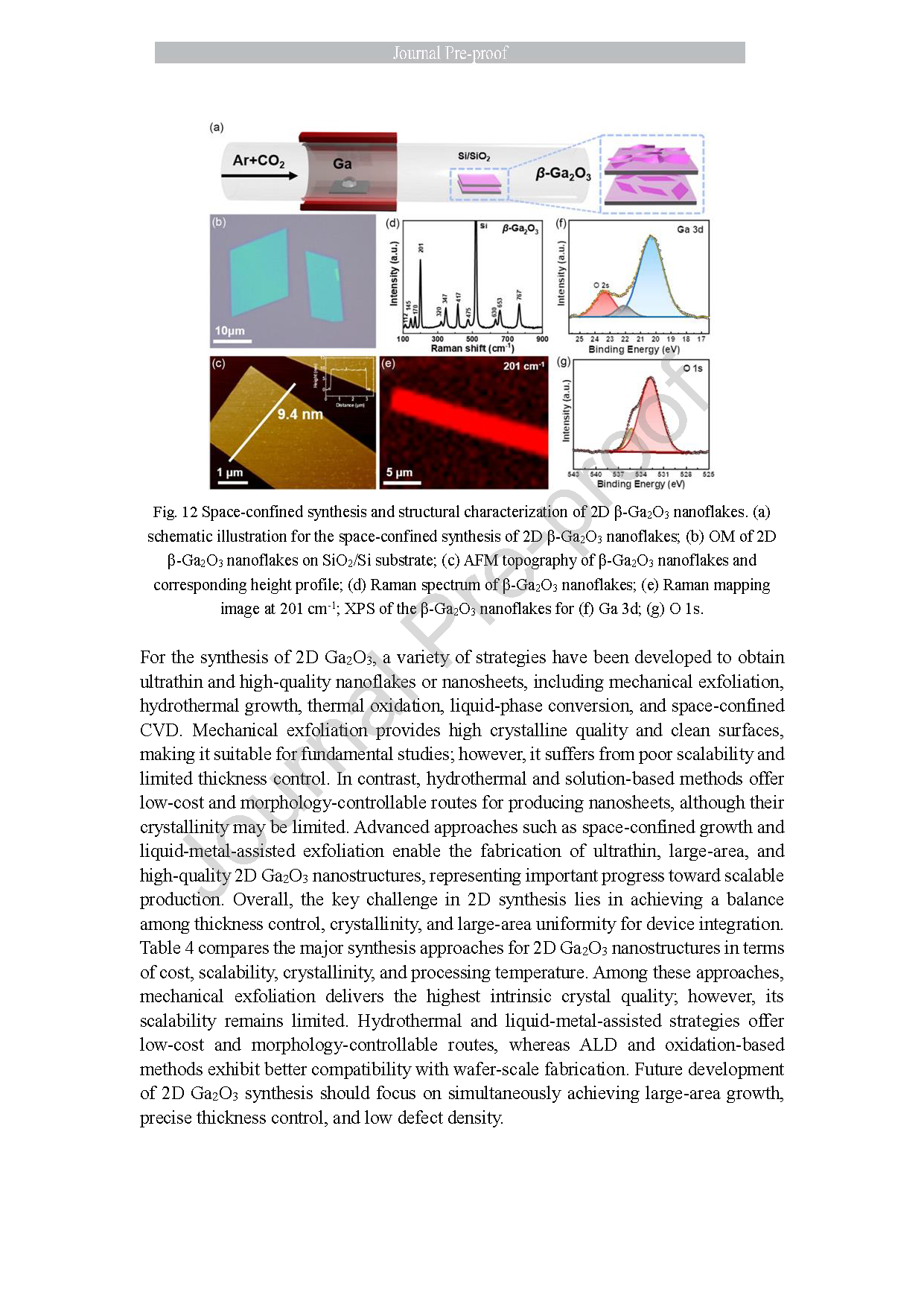
Fig. 12 Space-confined synthesis and structural characterization of 2D β-Ga₂O₃ nanoflakes. (a) schematic illustration for the space-confined synthesis of 2D β-Ga₂O₃ nanoflakes; (b) OM of 2D β-Ga₂O₃ nanoflakes on SiO₂/Si substrate; (c) AFM topography of β-Ga₂O₃ nanoflakes and corresponding height profile; (d) Raman spectrum of β-Ga₂O₃ nanoflakes; (e) Raman mapping image at 201 cm⁻¹; XPS of the β-Ga₂O₃ nanoflakes for (f) Ga 3d; (g) O 1s.
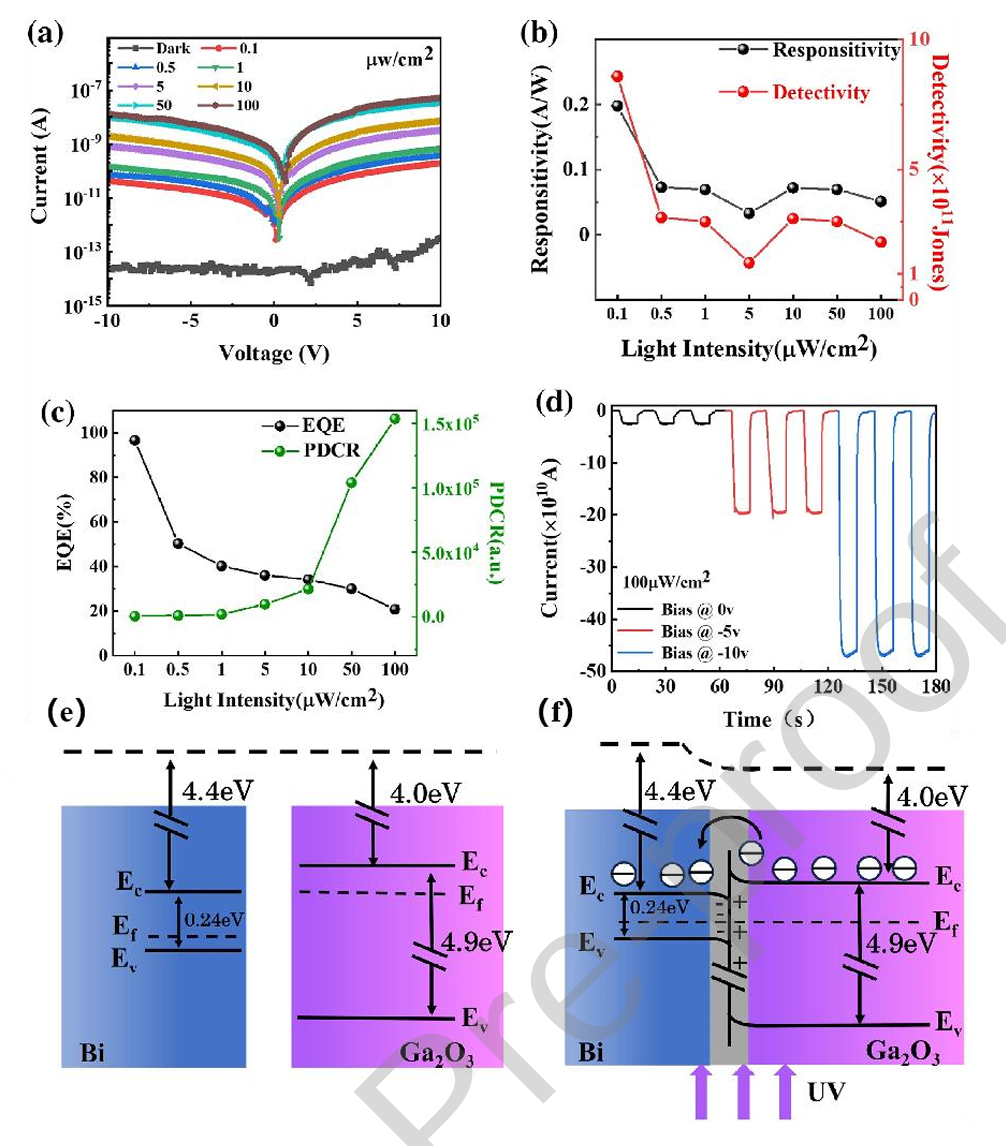
Fig. 13 Photodetection performance and interfacial band alignment mechanism of the Bi/Ga₂O₃ heterojunction photodetector. (a) I-V curves of the Bi/Ga₂O₃ heterojunction optoelectronic device under 254 nm illumination with various light intensities; (b) responsivity and specific detectivity of the Bi/Ga₂O₃ PD as a function of incident light intensity; (c) EQEs and PDCRs of the Bi/Ga₂O₃ PD at various light intensities; (d) Time-dependent current of the Bi/Ga₂O₃ PD at different bias voltages; (e) energy band diagram of Bi and Ga₂O₃ before contact; (f) energy band diagram of the Bi/Ga₂O₃ PD in forward bias under UV illumination.
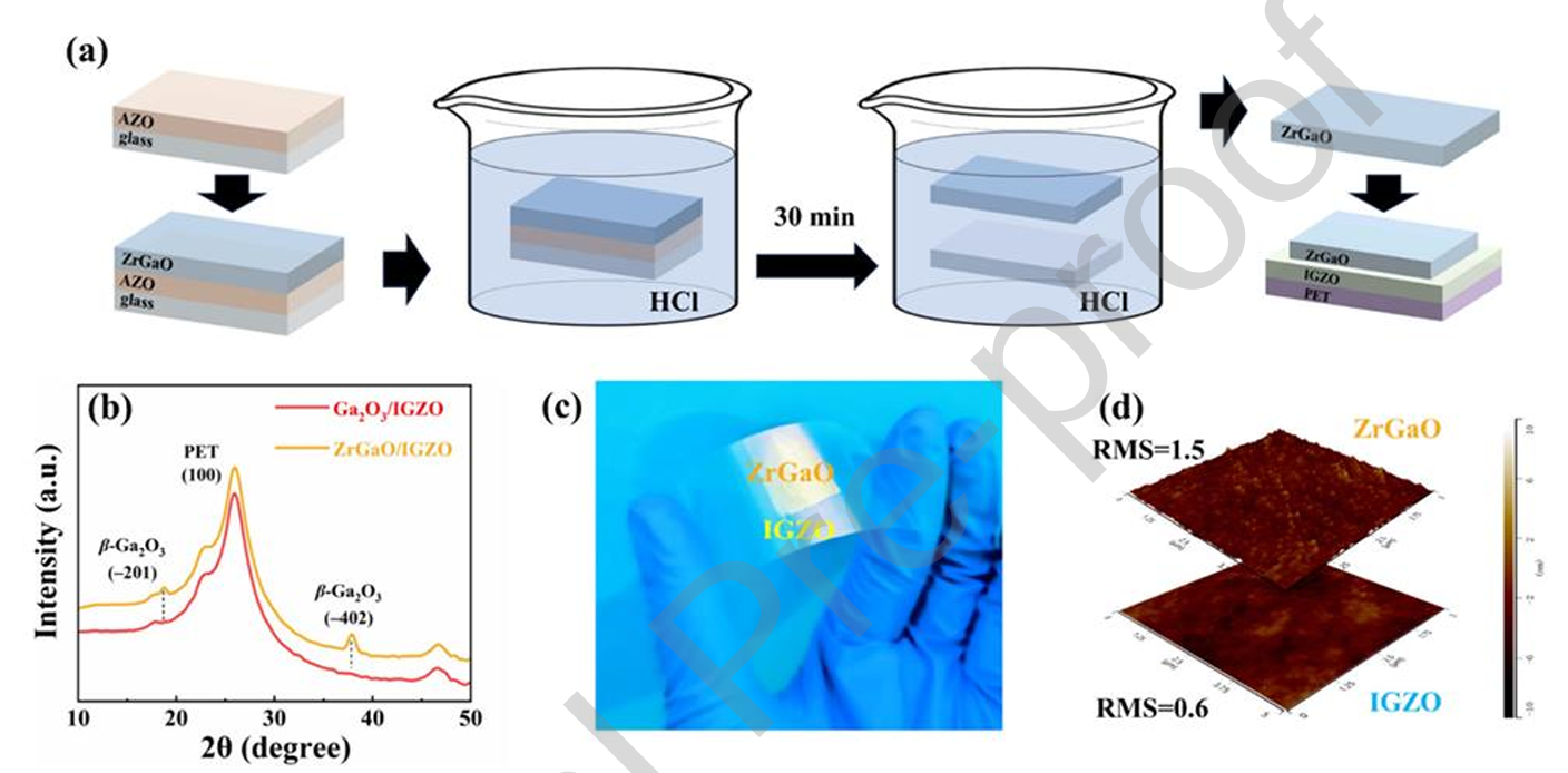
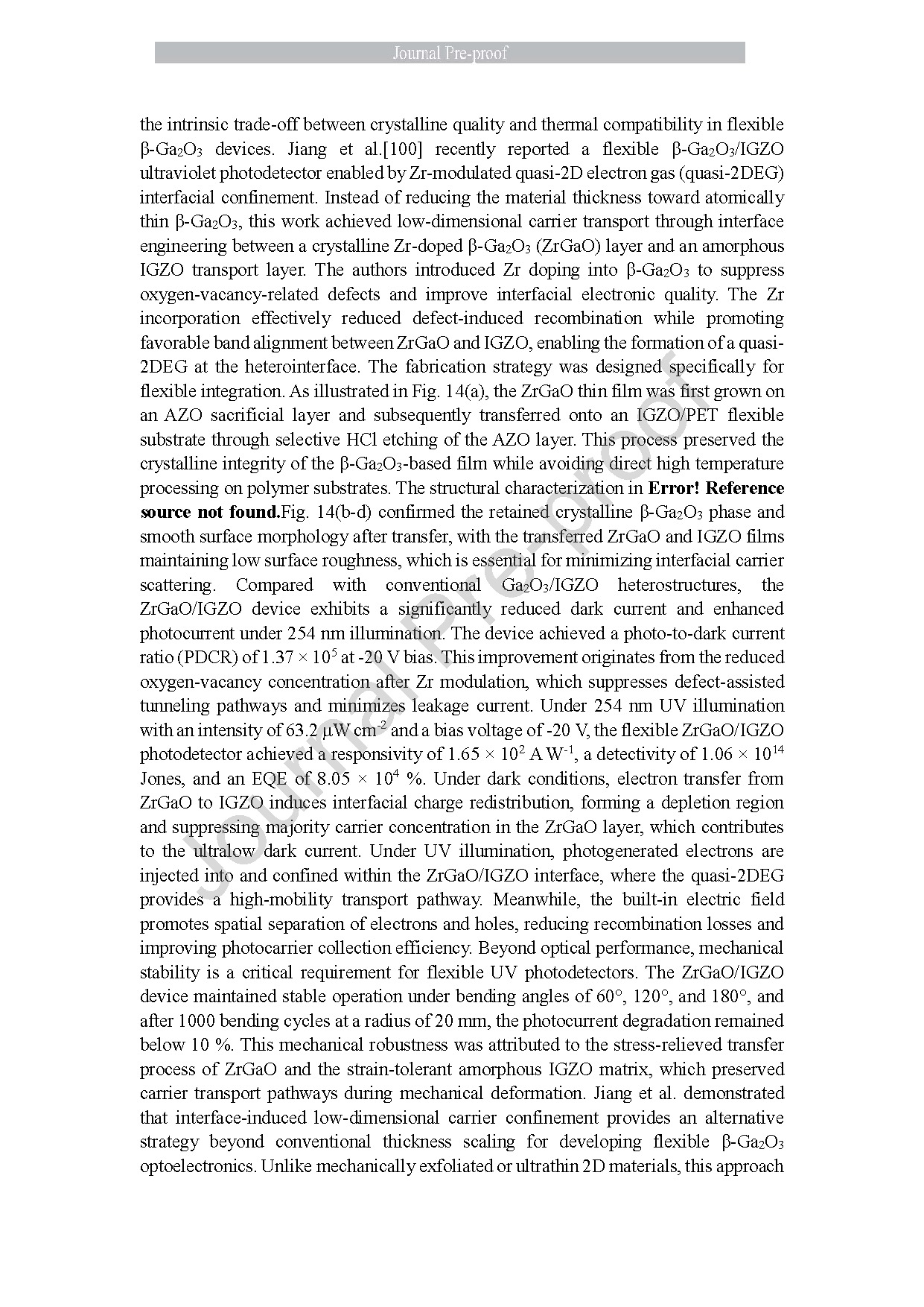
Fig. 14 Fabrication and structural characterization of transferred ZrGaO films on IGZO substrates. (a) schematic representation of the ZrGaO film transfer process onto IGZO substrates; (b) XRD patterns of Ga₂O₃/IGZO and ZrGaO/IGZO UVPDs; (c) optical photograph of ZrGaO films on IGZO substrates; (d) corresponding AFM images of ZrGaO and IGZO.
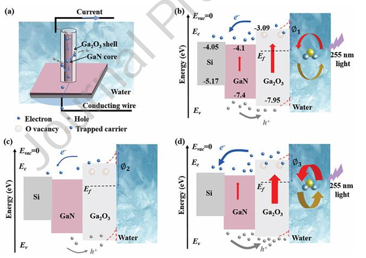
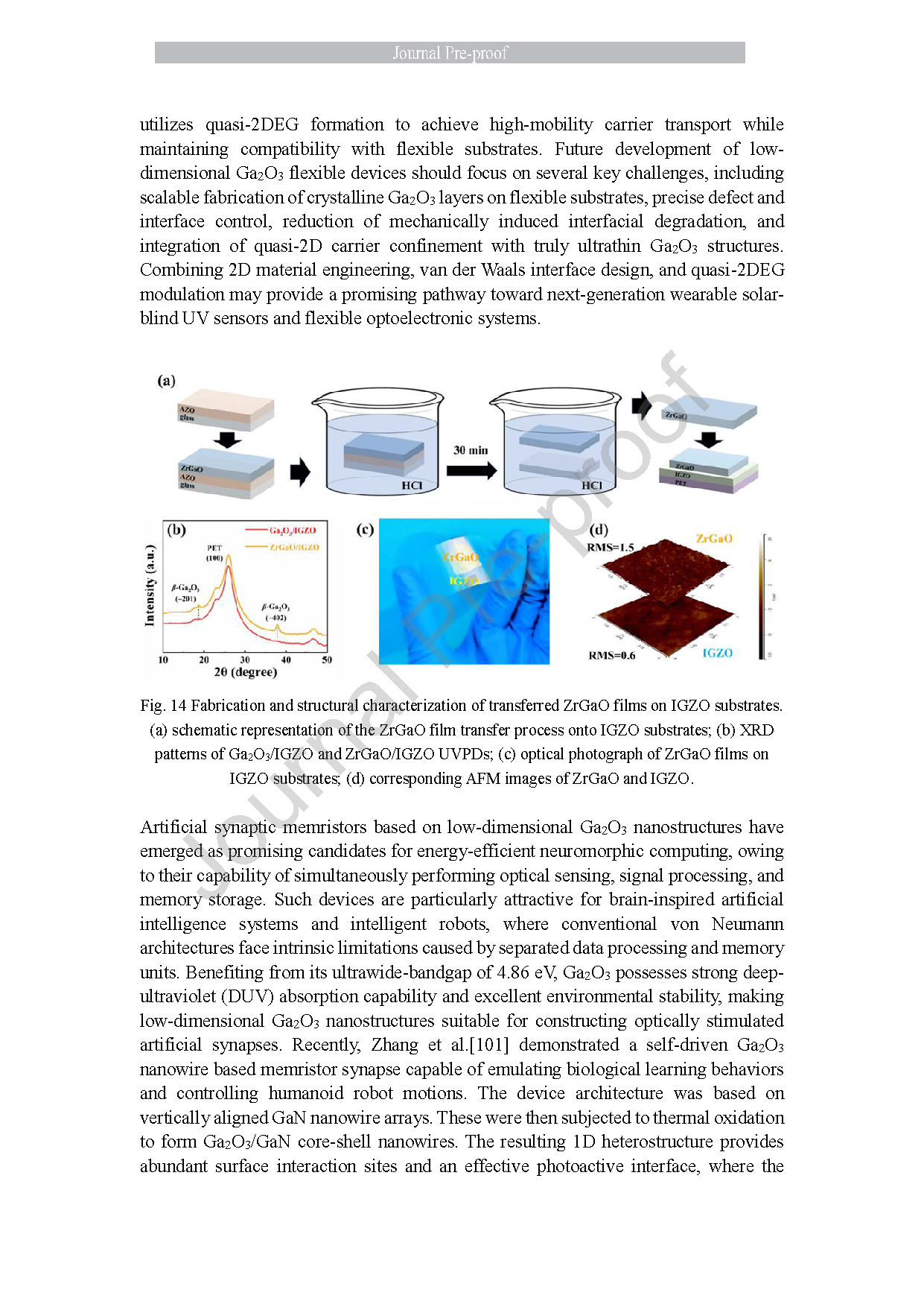
Fig. 15 Photoinduced carrier transport and oxygen vacancy-mediated synaptic mechanism in Ga₂O₃/GaN nanowire memristor synapses. (a) schematic illustration of artificial synaptic device under UV illumination; (b) schematic energy band diagram of the Ga₂O₃/GaN nanowires under the first 255 nm stimulation; (c) schematic energy band diagram of the Ga₂O₃/GaN nanowires without light stimulation;(d) schematic energy band diagram of the Ga₂O₃/GaN nanowires under the second 255 nm stimulation.
DOI:
doi.org/10.1016/j.jallcom.2026.191098










Instruction
Official Account

Cooperation
Top
