



Researchers from Cornell University have published a dissertation titled " A 7-eV bandgap semiconductor based on silicon-doped α-(AlₓGa₁₋ₓ)₂O₃ " in NATURE.
Background
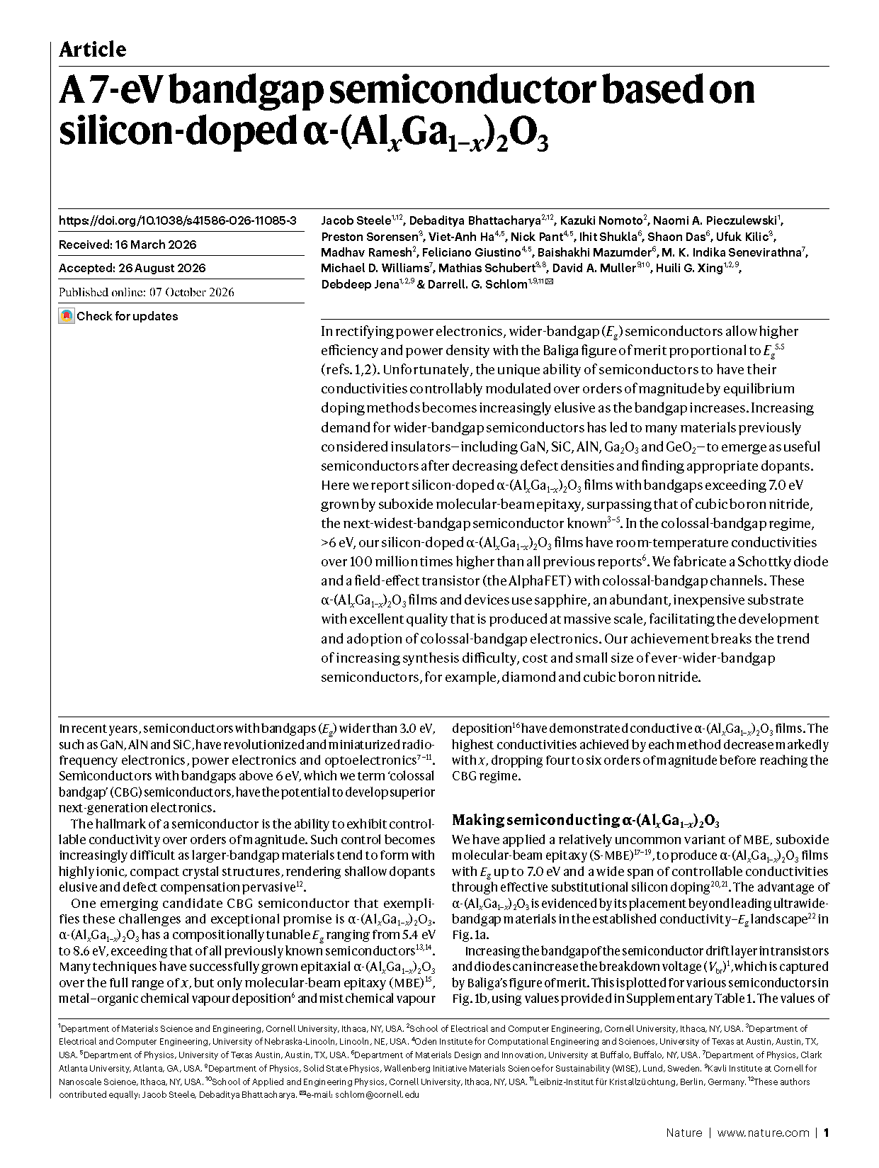
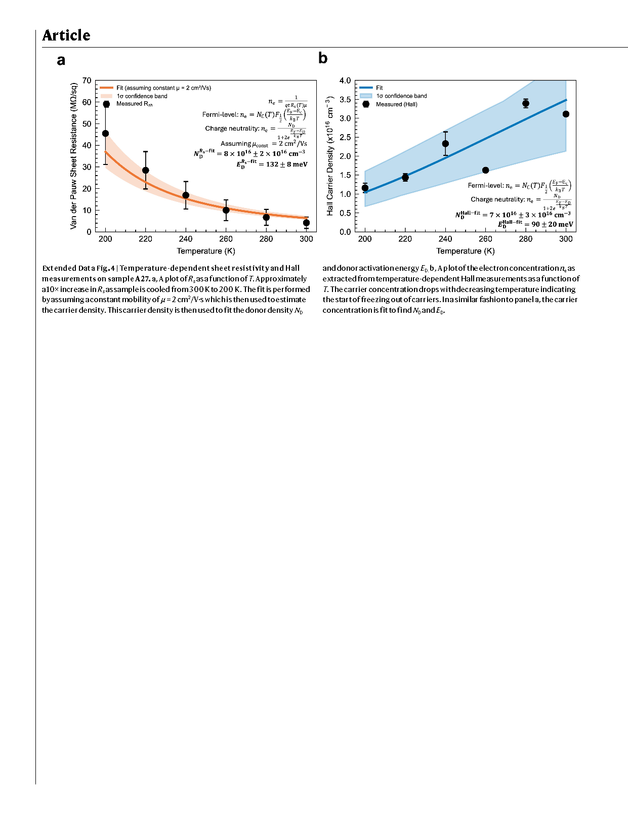
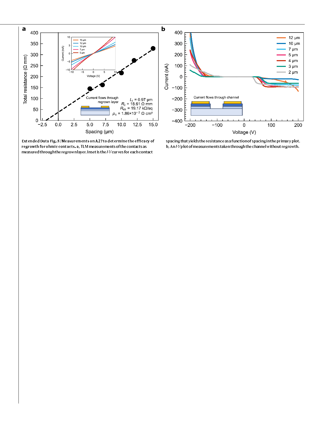
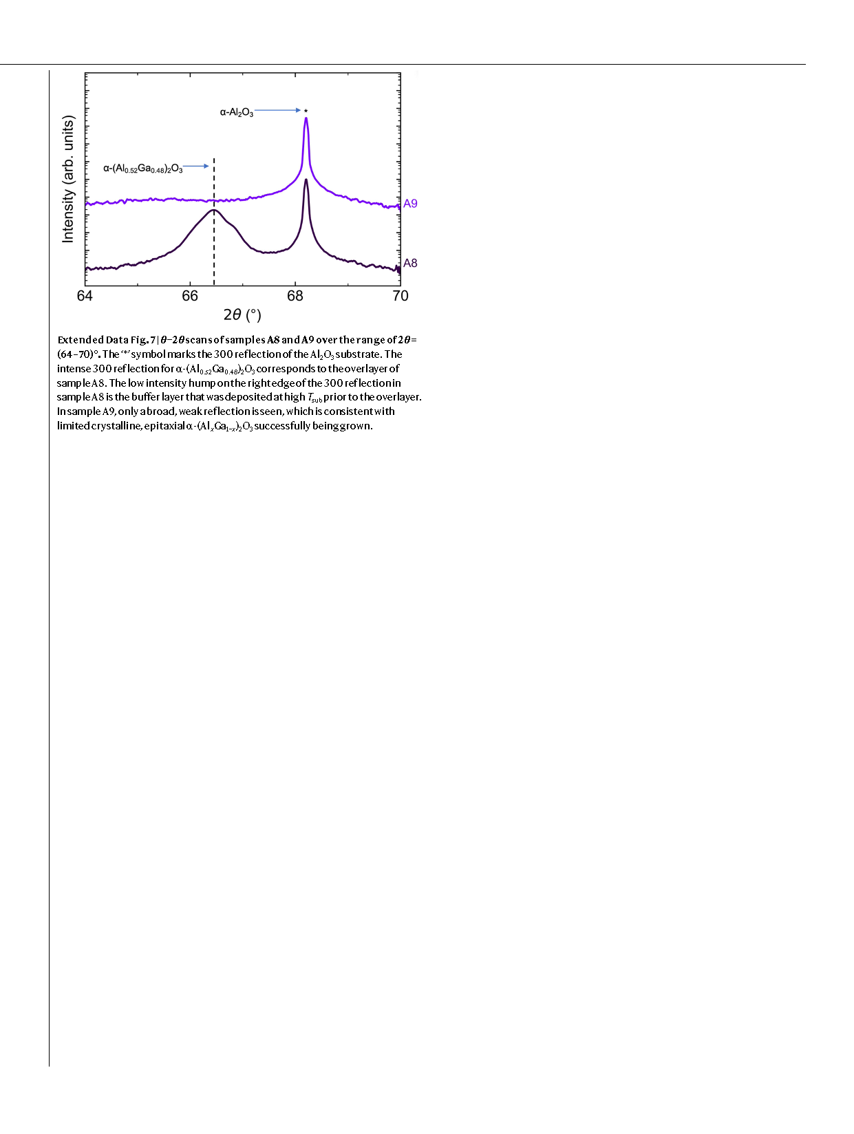
In recent years, semiconductors with bandgaps (Eg) wider than 3.0 eV, such as GaN, AlN and SiC, have revolutionized and miniaturized radio frequency electronics, power electronics and optoelectronics. Semiconductors with bandgaps above 6 eV, which we term ‘colossal bandgap’ (CBG) semiconductors, have the potential to develop superior next-generation electronics. The hallmark of a semiconductor is the ability to exhibit control lable conductivity over orders of magnitude. Such control becomes increasingly difficult as larger-bandgap materials tend to form with highly ionic, compact crystal structures, rendering shallow dopants elusive and defect compensation pervasive. One emerging candidate CBG semiconductor that exempli fies these challenges and exceptional promise is α-(AlₓGa₁₋ₓ)₂O₃. α-(AlₓGa₁₋ₓ)₂O₃ has a compositionally tunable Eg ranging from 5.4 eV to 8.6 eV, exceeding that of all previously known semiconductors. Many techniques have successfully grown epitaxial α-(AlₓGa₁₋ₓ)₂O₃ over the full range of x, but only molecular-beam epitaxy (MBE), metal–organic chemical vapour deposition6 and mist chemical vapour deposition have demonstrated conductive α-(AlₓGa₁₋ₓ)₂O₃ films. The highest conductivities achieved by each method decrease markedly with x, dropping four to six orders of magnitude before reaching the CBG regime.
Abstract
In rectifying power electronics, wider-bandgap (Eg) semiconductors allow higher efficiency and power density with the Baliga figure of merit proportional to Eg5.5. Unfortunately, the unique ability of semiconductors to have their conductivities controllably modulated over orders of magnitude by equilibrium doping methods becomes increasingly elusive as the bandgap increases. Increasing demand for wider-bandgap semiconductors has led to many materials previously considered insulators—including GaN, SiC, AlN, Ga₂O₃ and GeO₂—to emerge as useful semiconductors after decreasing defect densities and finding appropriate dopants. Here we report silicon-doped α-(AlₓGa₁₋ₓ)₂O₃ films with bandgaps exceeding 7.0 eV grown by suboxide molecular-beam epitaxy, surpassing that of cubic boron nitride, the next-widest-bandgap semiconductor known. In the colossal-bandgap regime, >6 eV, our silicon-doped α-(AlₓGa₁₋ₓ)₂O₃ films have room-temperature conductivities over 100 million times higher than all previous reports. We fabricate a Schottky diode and a field-effect transistor (the AlphaFET) with colossal-bandgap channels. These α-(AlₓGa₁₋ₓ)₂O₃ films and devices use sapphire, an abundant, inexpensive substrate with excellent quality that is produced at massive scale, facilitating the development and adoption of colossal-bandgap electronics. Our achievement breaks the trend of increasing synthesis difficulty, cost and small size of ever-wider-bandgap semiconductors, for example, diamond and cubic boron nitride.
Conclusion
Although simple, these illustrative devices demonstrate current rectification in Schottky diode structures, and electrostatic gating of the channel in a three-terminal transistor geometry. To our knowledge, these results demonstrate the widest-Eg semiconductor in which active electronic device behaviour utilizing controlled carrier transport and field-effect modulation has been achieved. With the facile availability of sapphire substrates, our results lay the groundwork for the development of α-(AlₓGa₁₋ₓ)₂O₃-based CBG channel power and optoelectronic devices. The insights gained from this study highlight the key limitations of the present device implementations, including contact injection and access resistance. These challenges can be addressed through established epitaxial design and fabrication strategies including com positional grading, optimized contact engineering and improved electrostatic control. Improved device design and bandgap engineering within the α-(AlₓGa₁₋ₓ)₂O₃ system is expected to lead to vertical devices with even larger breakdown voltages and lower on-resistance. We anticipate that the large, tunable Eg of α-(AlₓGa₁₋ₓ)₂O₃ will be used for tunable deep-ultraviolet photonics and that the large band offsets will enable both absorbing and emitting photonics utilizing intersubband transitions for improved operational frequencies.
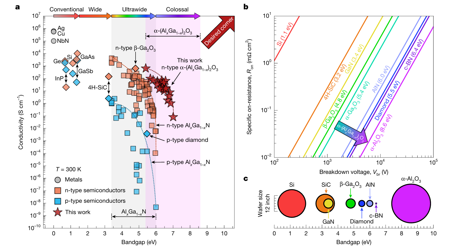
Fig. 1 | Benchmarking α-(AlₓGa₁₋ₓ)₂O₃. a, A comparison of the highest reported conductivities as a function of bandgap for select metals and semiconductors. The values for 22 of our α-(AlₓGa₁₋ₓ)₂O₃ thin films, samples A2–A8 and A11–A25, are marked by red stars. The dashed lines are the fitted trends in conductivity versus bandgap for alloy semiconductors. b, An analytical plot of the on-resistance versus breakdown curves of various semiconductors. The lines are contours of constant Baliga’s figure of merit for each material. The multicolour arrow shows the theoretical range covered by α-(AlₓGa₁₋ₓ)₂O₃ alloys. c, A diagram showing the largest-diameter synthetic crystals for various semiconductor substrates with the centre of each circle located at the material’s bandgap.
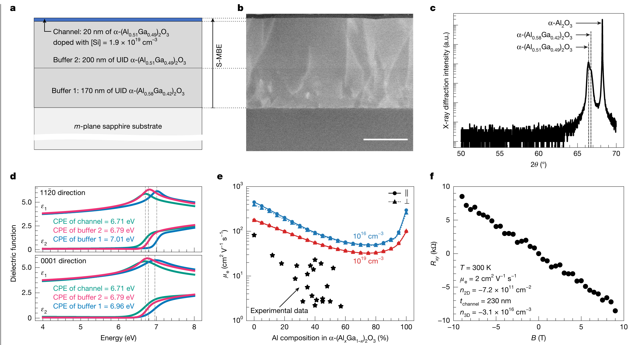
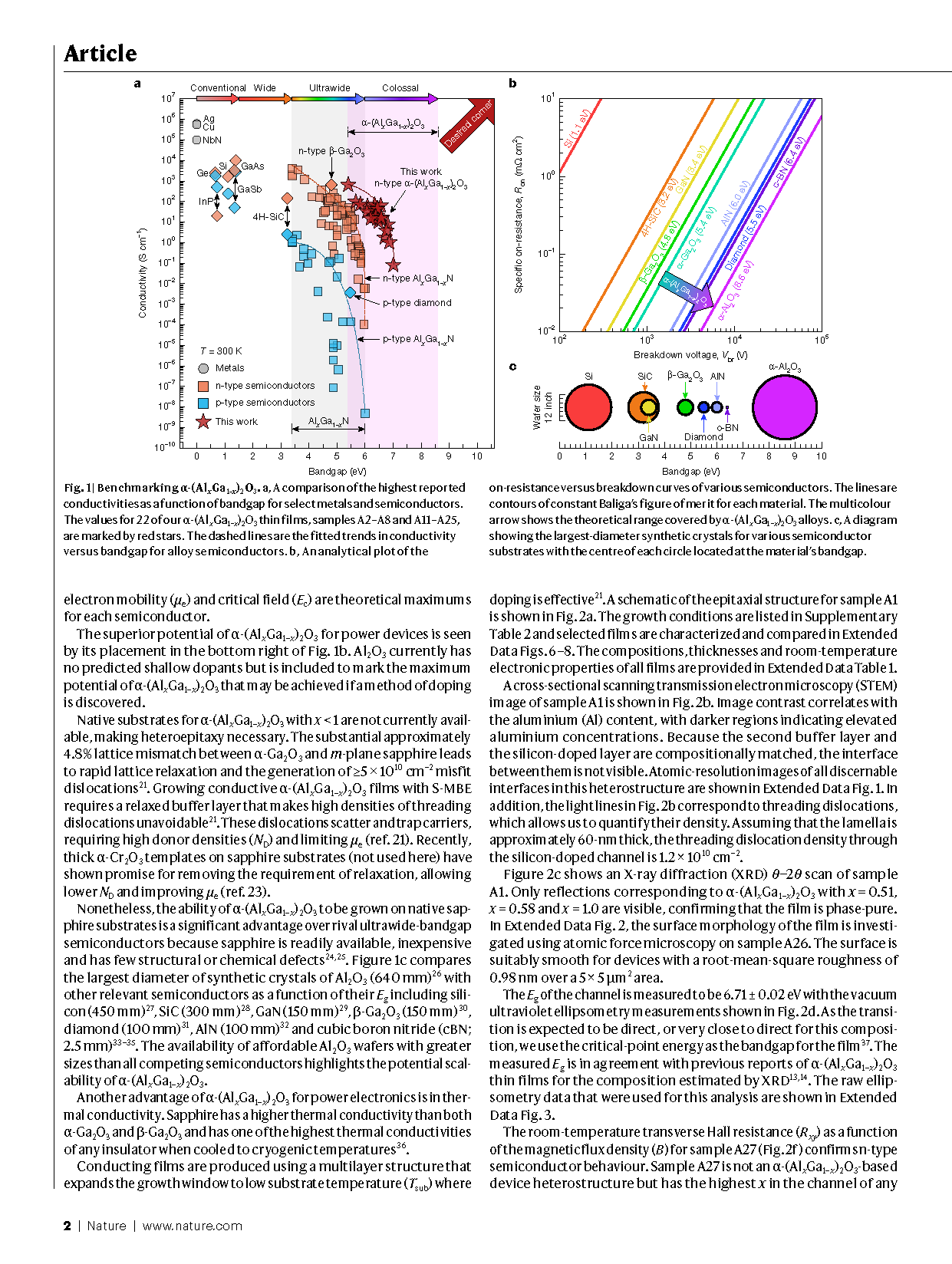
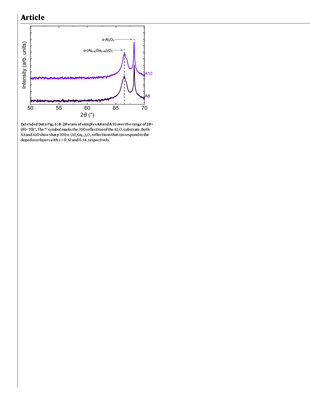
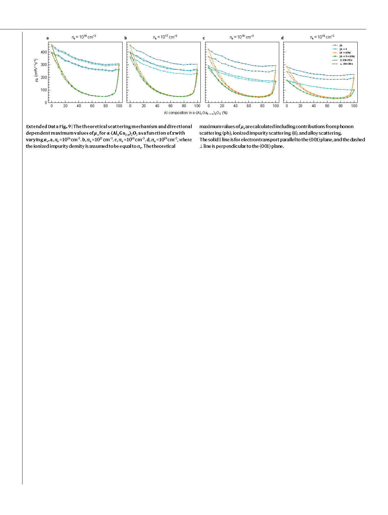
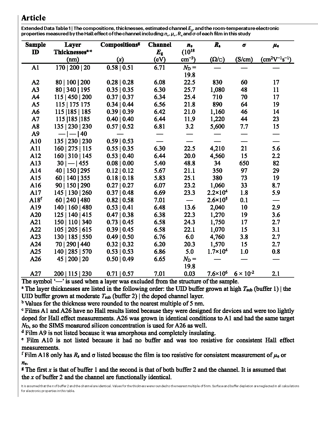
Fig. 2 | Characterization of as-grown α-(AlₓGa₁₋ₓ)₂O₃.a, Schematic of the as-grown epitaxial film structure of sample A1. UID, unintentionally doped.b, Cross-sectional STEM image of sample A1. The layers and interfaces are vertically aligned to those in a. Scale bar, 200 nm. c, An XRD θ−2θ scan of sample A1 over the range 2θ = (50–70)°. The dashed lines mark the 300 reflections of the α-(AlₓGa₁₋ₓ)₂O₃ film layers.d, Plot of the real (ε₁) and imaginary (ε₂) dielectric function components along [1120] and [0001] directions. CPE, critical-point energy. e, A plot of the theoretical maximum µe as a function of x for values of ND = 10¹⁶ cm⁻³ and ND = 10¹⁹ cm⁻³ plotted as blue and red lines, respectively. The solid lines with circular points represent the electron mobility parallel to the (001) plane and the dashed lines with triangular markers reflect the electron mobility perpendicular to the (001) plane. The theoretical maximum mobilities are calculated using the contributions of ionized impurity, phonon and alloy scattering. The Hall µe of 21 of our S-MBE grown α-(AlₓGa₁₋ₓ)₂O₃ films (samples A2–A8, A11–A17, A19–A24 and A27) are plotted with star symbols. The majority of the α-(AlₓGa₁₋ₓ)₂O₃ films plotted have ND≈ (2.3±0.3) × 10¹⁹ cm⁻³. f, The room temperature transverse Hall resistance (Rxy) as a function of magnetic flux density (B) of sample A27, which gives the 2D mobile carrier density, n2D. The 3D mobile carrier density, n3D, is determined by dividing n2D by the thickness of the channel layer, tchannel.
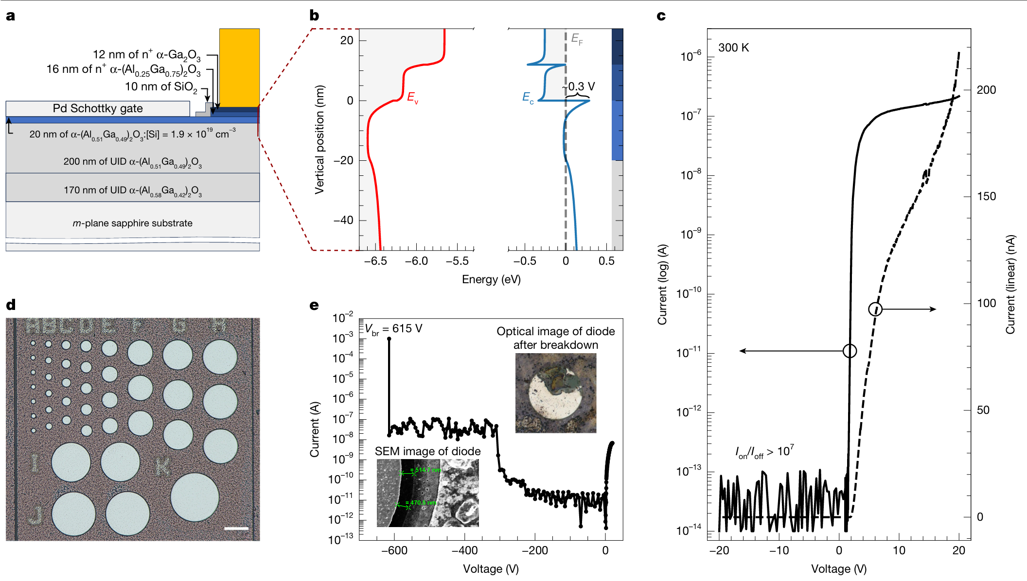
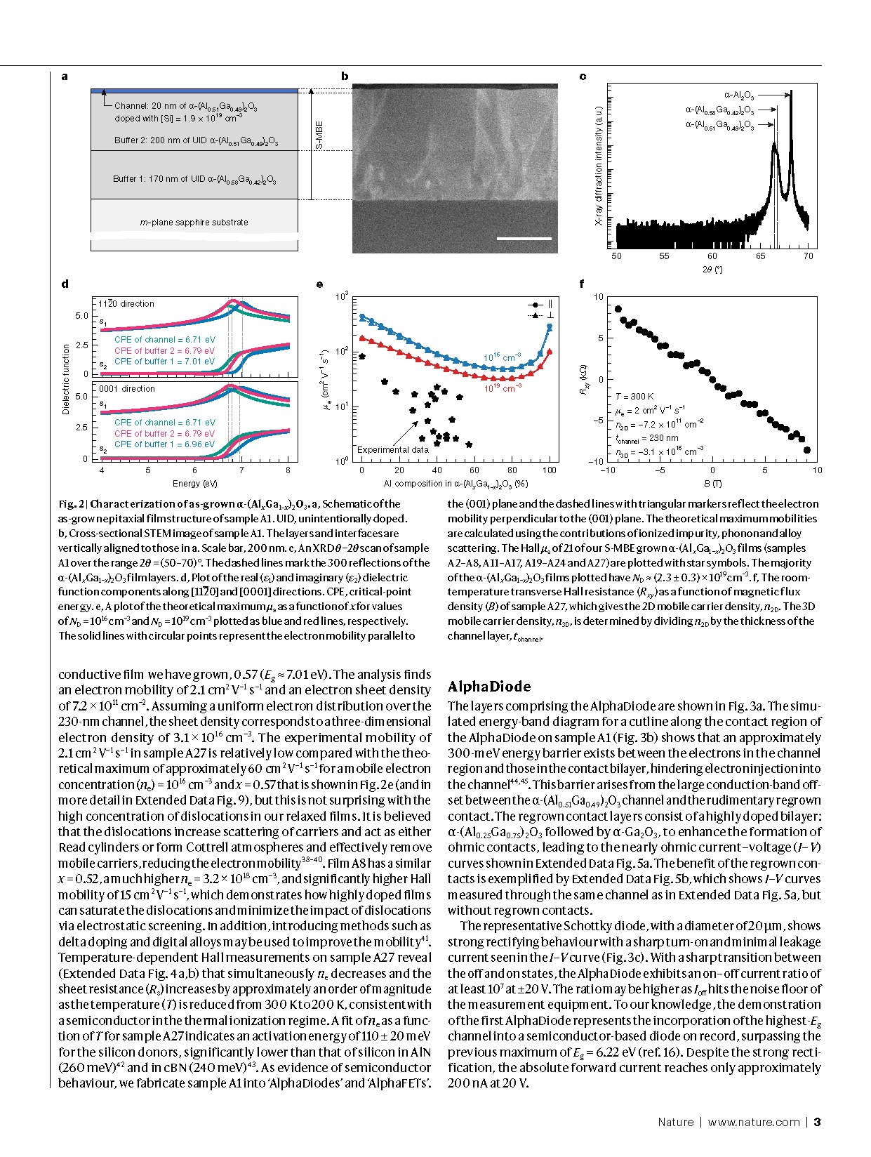
Fig. 3 | Electrical characteristics of an AlphaDiode. a, Schematic of the fully fabricated AlphaDiode. The epitaxial structure consists of the as-grown sample in Fig. 2a. b, Energy-band diagram of the vertical cross-section of the device underneath the contact as shown by the red line in a. The solid red line and blue line in b represent the energies of the valence band edge (Ev) and the conduction band edge (Ec), respectively, and the dashed grey line marks the Fermi level (EF) throughout the device. The zero of the vertical axis corresponds to the surface of the channel layer. c, I–V characteristics of an AlphaDiode with 20 µm diameter. d, An optical microscope image of processed AlphaDiodes. Scale bar, 50 µm.e, Reverse-breakdown measurements performed on a representative AlphaDiode with 60 µm diameter. Bottom-left inset: SEM image showing the minimum spacing between the anode and the regrown contact layers. Top-right inset: the device after breakdown.
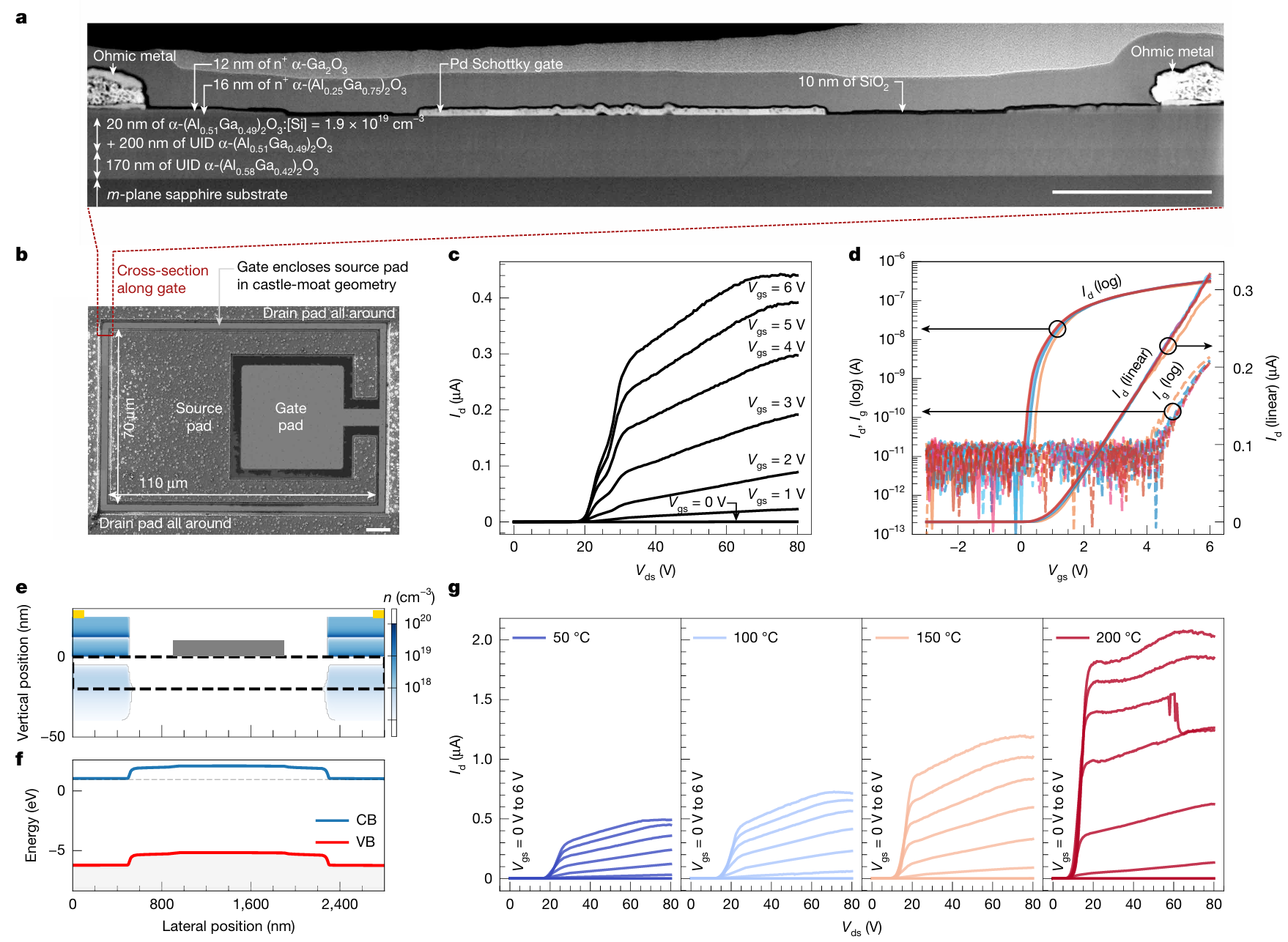
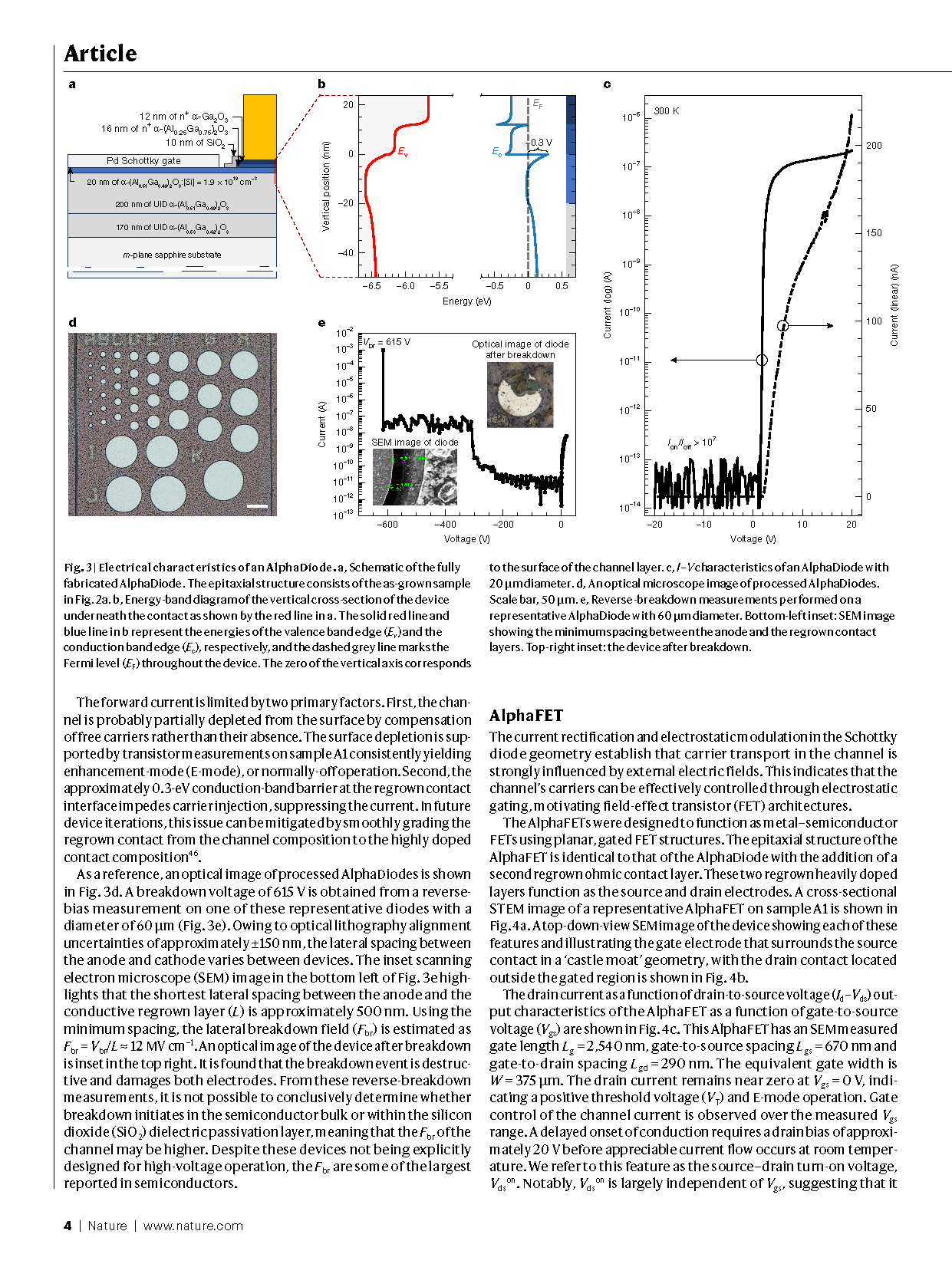
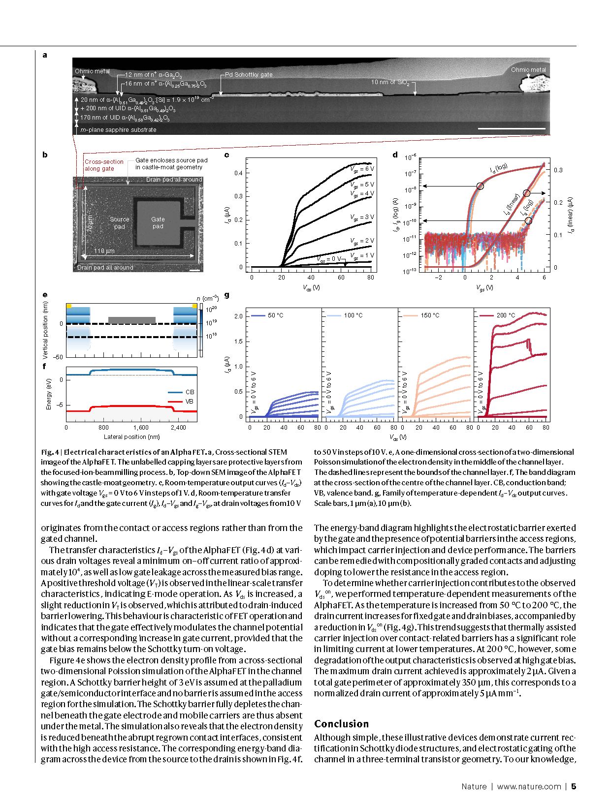
Fig. 4 | Electrical characteristics of an AlphaFET.a, Cross-sectional STEM image of the AlphaFET. The unlabelled capping layers are protective layers from the focused-ion-beam milling process.b, Top-down SEM image of the AlphaFET showing the castle-moat geometry.c, Room-temperature output curves (Id–Vds) with gate voltage Vgs = 0 V to 6 V in steps of 1 V.d, Room-temperature transfer curves for Id and the gate current (Ig), Id–Vgs and Ig–Vgs, at drain voltages from 10 V to 50 V in steps of 10 V. e, A one-dimensional cross-section of a two-dimensional Poisson simulation of the electron density in the middle of the channel layer. The dashed lines represent the bounds of the channel layer.f, The band diagram at the cross-section of the centre of the channel layer. CB, conduction band; VB, valence band.g, Family of temperature-dependent Id–Vds output curves. Scale bars, 1 µm (a), 10 µm (b).
DOI:
doi.org/10.1038/s41586-026-11085-3

Instruction
Official Account

Cooperation
Top
