


Researchers from Nanjing University、Suzhou Institute of Nano-Tech and Nano-Bionics and The University of Hong Kong have published a dissertation titled " Nitrogen-graded electrostatic compensation for normally-off β-Ga₂O₃ planar-gate current-aperture vertical electron transistors " in Applied Physics Letters.
Background
Gallium oxide (Ga₂O₃) is an emerging ultra-wide bandgap semiconductor for next-generation high-voltage and high-power electronics. In particular, recent demonstrations of megawatt-class pulsed switching at 1kV and 1kA highlight its unique capability for pulse power applications. Nevertheless, the absence of reliable p-type Ga₂O₃ fundamentally limits the realization of bipolar device architectures, making normally-off operation in vertical β-Ga₂O₃ transistors primarily dependent on electrostatic channel engineering.
Abstract
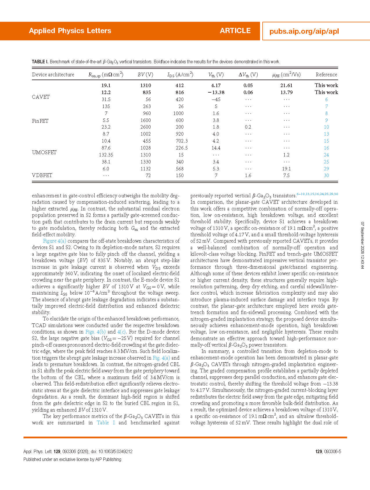
Gallium oxide (Ga₂O₃) vertical transistors are promising for next-generation high-voltage power electronics, yet achieving normally-off operation remains challenging due to insufficient electrostatic depletion of the surface channel and severe gate-edge electric-field crowding. Here, we demonstrate a controlled transition from depletion-mode to enhancement-mode operation in all-ion-implanted planar-gate β-Ga₂O₃ current-aperture vertical electron transistors, a gate region-damage-minimized architecture that avoids gate-trench etching. A multi-step nitrogen-graded current-blocking layer (CBL) simultaneously engineers channel electrostatics and high-voltage electric-field distributions by introducing vertically distributed charge compensation. This graded profile enhances subsurface channel depletion, suppresses parallel conduction, and redistributes the peak electric field from the gate edge toward the buried CBL. As a result, the enhancement-mode device achieves a threshold voltage of 4.17V, a breakdown voltage of 1310 V, a specific on-resistance of 19.1 mΩcm2, and an ultralow threshold hysteresis of 52 mV. These results establish nitrogen-graded electrostatic compensation as an effective strategy for simultaneously realizing normally-off operation and enhanced voltage-blocking capability in vertical β-Ga₂O₃ transistors.
Conclusion
In summary, a controlled transition from depletion-mode to enhancement-mode operation has been demonstrated in planar-gate β-Ga₂O₃ CAVETs through nitrogen-graded implantation engineering. The graded compensation profile establishes a partially depleted channel, suppresses deep parallel conduction, and enhances gate electrostatic control, thereby shifting the threshold voltage from −13.38 to 4.17 V. Simultaneously, the nitrogen-graded current-blocking layer redistributes the electric field away from the gate edge, mitigating field crowding and promoting a more favorable bulk-field distribution. As a result, the optimized device achieves a breakdown voltage of 1310 V, a specific on-resistance of 19.1mΩcm2, and an ultralow threshold- voltage hysteresis of 52mV. These results highlight the dual role of nitrogen-graded implantation in simultaneously engineering channel electrostatics and high-voltage electric-field distributions, providing an effective pathway toward high-performance normally-off vertical β-Ga₂O₃ power transistors.
Project Support
This work was supported by the National Natural Science Foundation of China (Nos. 62425403 and 62234007) and the Jiangsu Provincial Science and Technology Major Project (No. BG2024030).
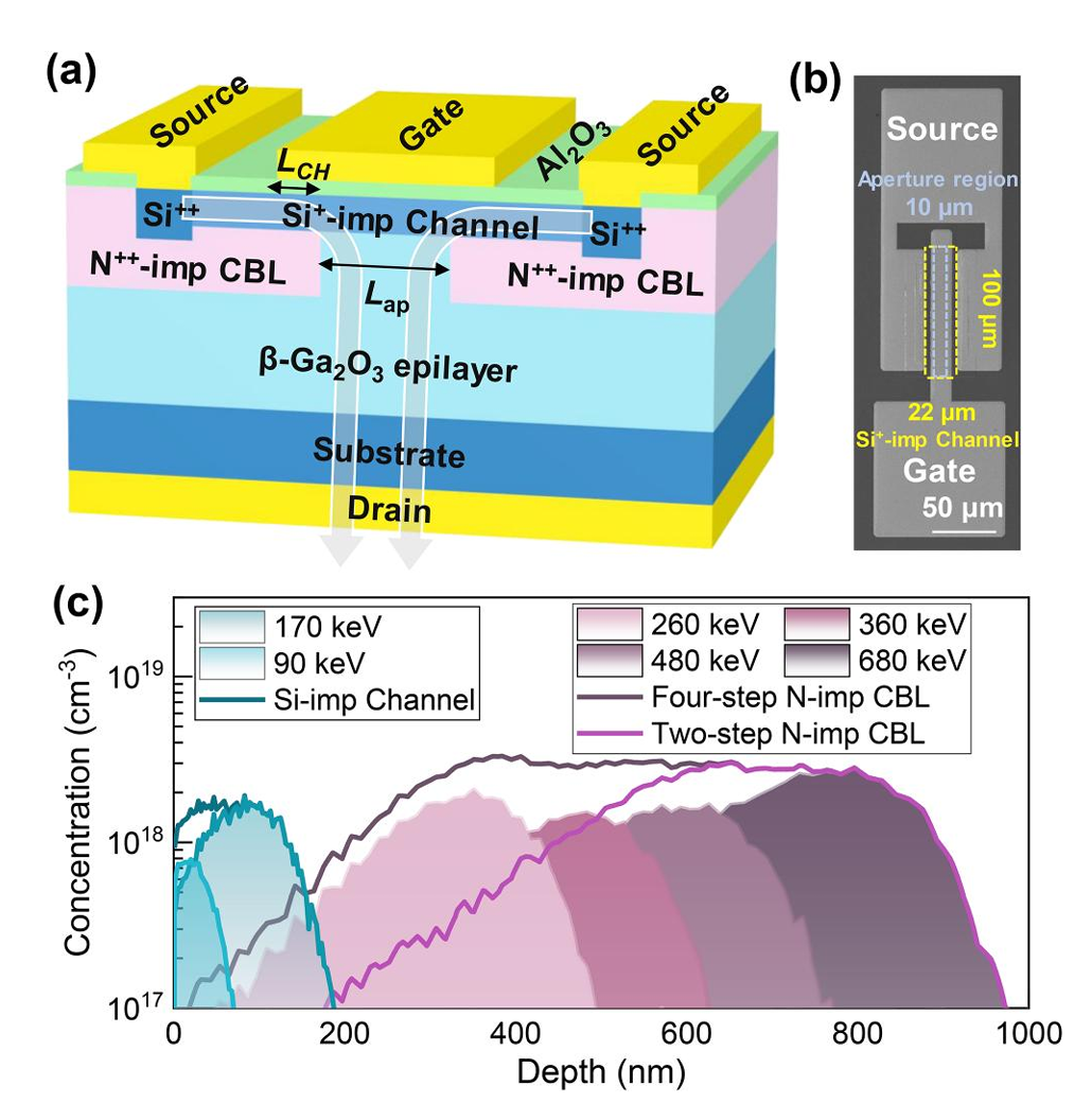
FIG. 1. (a) Schematic illustration and (b) optical micrograph of the β-Ga₂O₃ planar-gate CAVET. The arrows in (a) indicate the carrier transport path from the source to the drain through the current aperture (Lap) defined by the current- blocking layer. (c) SRIM-simulated depth profiles of the multi-energy Si implantation in the channel region and the N implantation in the CBL.
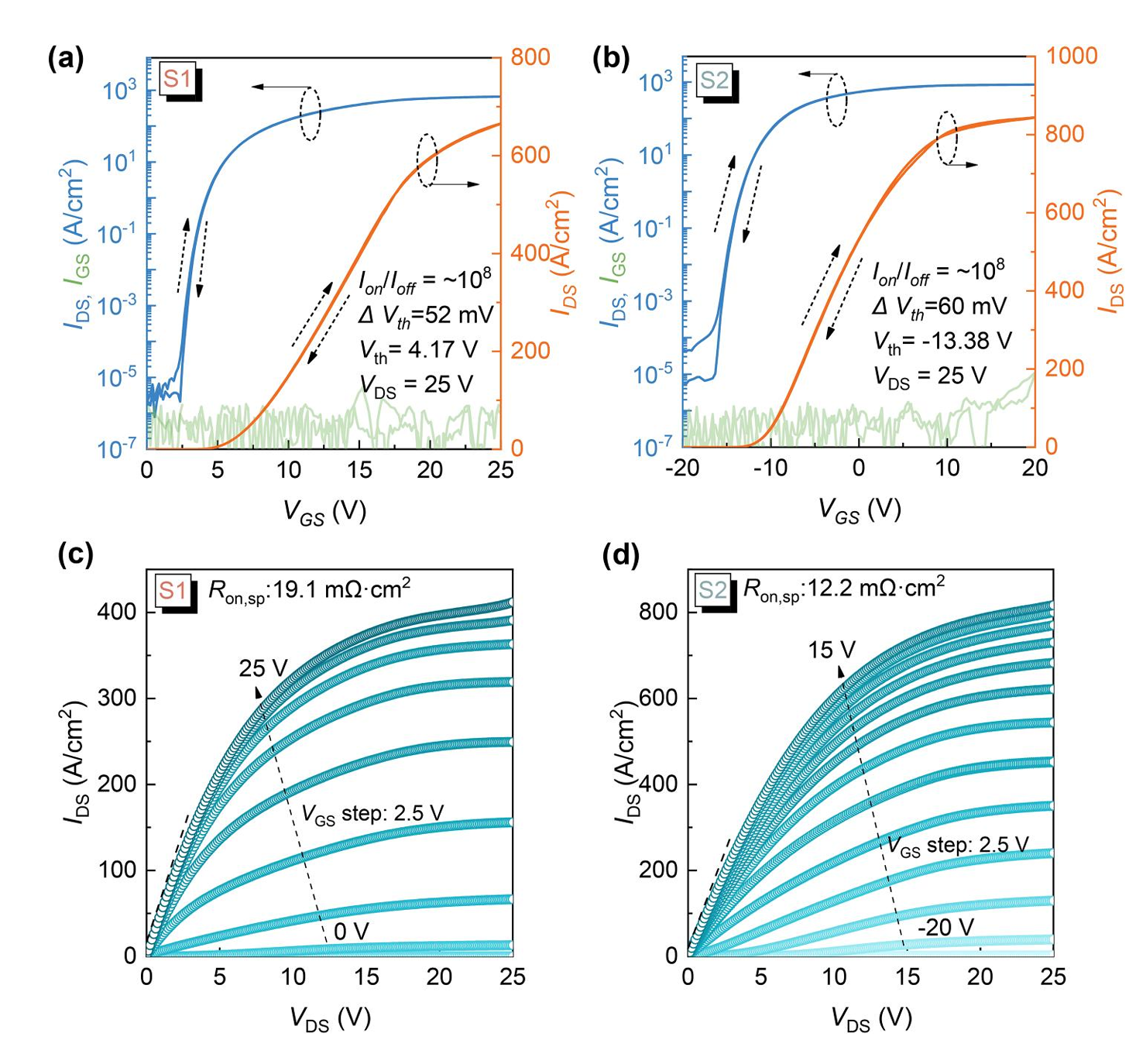
FIG. 2. Transfer characteristics (IDS–VGS) of devices S1 (a) and S2 (b) plotted on both linear and logarithmic scales, together with IGS as a function of VGS. Output characteristics (IDS–VDS) of devices S1 (c) and S2 (d).
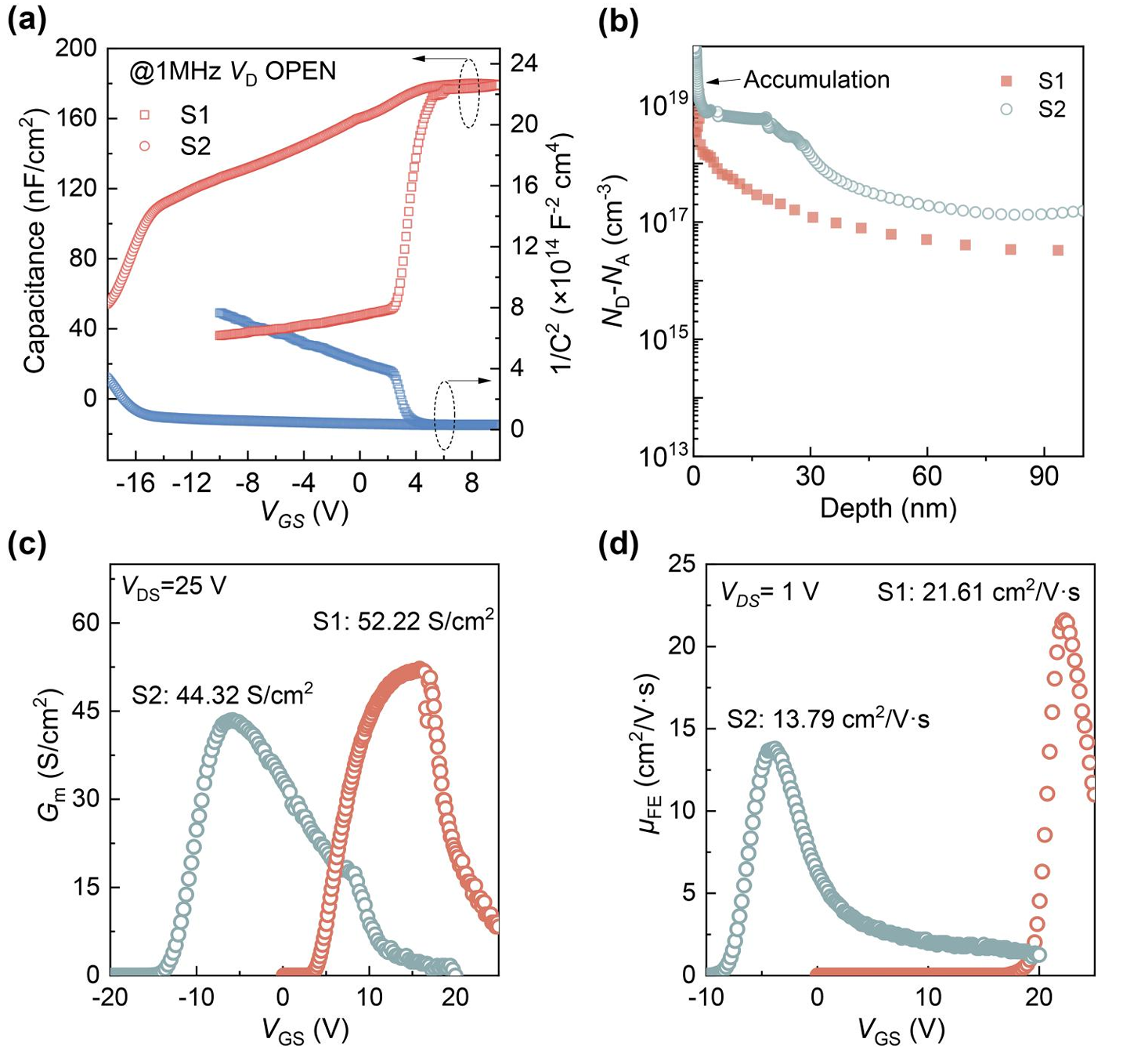
FIG. 3. (a) The gate-to-source capacitance–voltage (C–V) and 1/C2–V characteristics of devices S1 and S2; (b) the extracted carrier concentration profiles underneath the gate regions of S1 and S2; and (c) transconductance (Gm) and (d) the extracted field-effect mobility (uFE) as a function of VGS for devices S1 and S2.
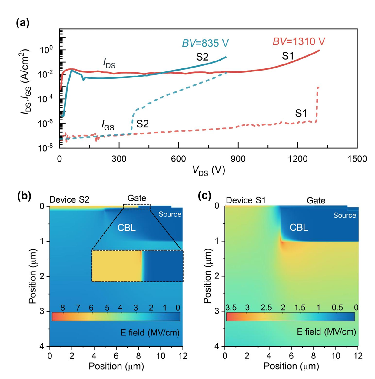
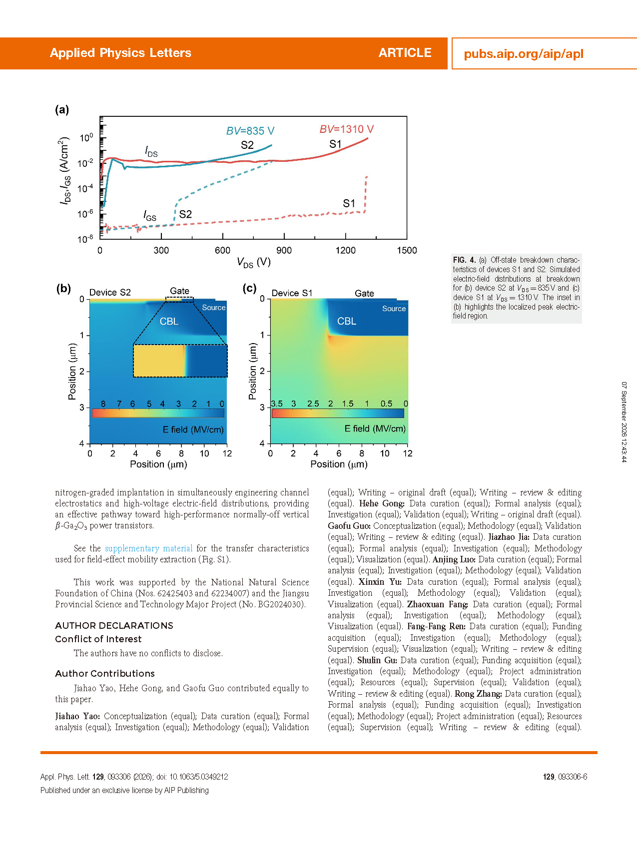
FIG. 4. (a) Off-state breakdown characteristics of devices S1 and S2. Simulated electric-field distributions at breakdown for (b) device S2 at VDS = 835V and (c) device S1 at VDS=1310V. The inset in (b) highlights the localized peak electric-field region.
DOI:
doi.org/10.1063/5.0349212
Instruction
Official Account

Cooperation
Top
