


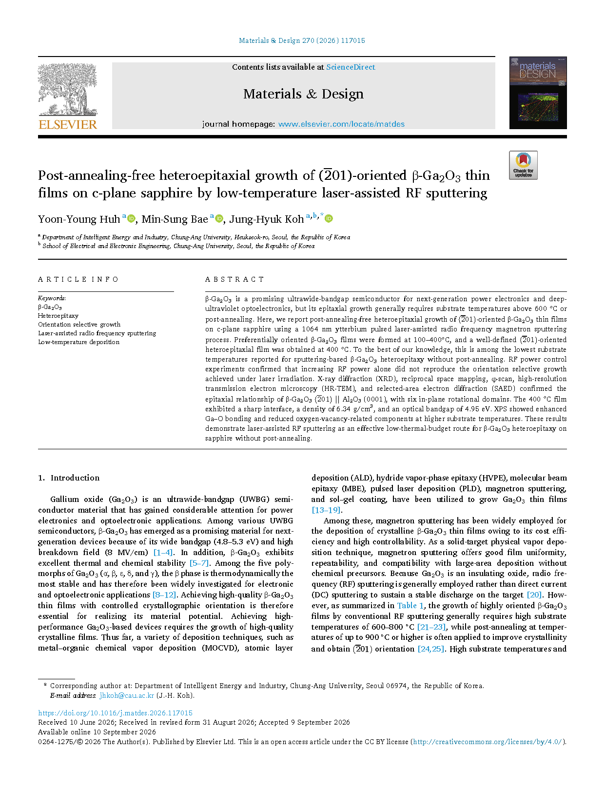
Researchers from the Chung‑Ang University, the Republic of Korea have published a dissertation titled "Post‑annealing‑free heteroepitaxial growth of (201)‑oriented β-Ga₂O₃ thin films on c‑plane sapphire by low‑temperature laser‑assisted RF sputtering" in Materials & Design.
Background
Gallium oxide (Ga₂O₃) is an ultrawide-bandgap (UWBG) semiconductor material that has gained considerable attention for power electronics and optoelectronic applications, with β-Ga₂O₃ being the most thermodynamically stable and promising candidate. Achieving high-quality β-Ga₂O₃ thin films with controlled crystallographic orientation is essential for realizing high-performance devices. Various deposition techniques such as MOCVD, ALD, HVPE, MBE, PLD, magnetron sputtering, and sol-gel coating have been utilized. Among these, magnetron sputtering is widely employed for its cost efficiency and high controllability. However, conventional RF sputtering generally requires high substrate temperatures of 600–800 °C and post-annealing at up to 900 °C or higher to obtain (-201) orientation, which prolongs processing time, increases energy consumption, and may degrade film quality. Therefore, a deposition strategy capable of achieving epitaxial alignment under a reduced thermal budget is essential. To address this challenge, the team employs a laser-assisted RF sputtering technique in which a 1064 nm ytterbium pulsed laser is applied in situ during film growth. This study applies this method for the first time to low-temperature, post-annealing-free β-Ga₂O₃ heteroepitaxial growth on c-plane sapphire, depositing (-201)-oriented films at substrate temperatures from RT to 400 °C without post-annealing.
Abstract
β-Ga₂O₃ is a promising ultrawide-bandgap semiconductor for next-generation power electronics and deep-ultraviolet optoelectronics, but its epitaxial growth generally requires substrate temperatures above 600 °C or post-annealing. Here, we report post-annealing-free heteroepitaxial growth of (-201)-oriented β-Ga₂O₃ thin films on c-plane sapphire using a 1064 nm ytterbium pulsed laser-assisted radio frequency magnetron sputtering process. Preferentially oriented β-Ga₂O₃ films were formed at 100-400 °C, and a well-defined (-201)-oriented heteroepitaxial film was obtained at 400 °C. To the best of our knowledge, this is among the lowest substrate temperatures reported for sputtering-based β-Ga₂O₃ heteroepitaxy without post-annealing. RF power control experiments confirmed that increasing RF power alone did not reproduce the orientation selective growth achieved under laser irradiation. X-ray diffraction (XRD), reciprocal space mapping, φ-scan, high-resolution transmission electron microscopy (HR-TEM), and selected-area electron diffraction (SAED) confirmed the epitaxial relationship of β-Ga₂O₃ (-201) ‖ Al₂O₃ (0001), with six in-plane rotational domains. The 400 °C film exhibited a sharp interface, a density of 6.34 g/cm³, and an optical bandgap of 4.95 eV. XPS showed enhanced Ga-O bonding and reduced oxygen-vacancy-related components at higher substrate temperatures. These results demonstrate laser-assisted RF sputtering as an effective low-thermal-budget route for β-Ga₂O₃ heteroepitaxy on sapphire without post-annealing.
Highlights
Post-annealing-free low-temperature heteroepitaxy: The team achieved post-annealing-free heteroepitaxial growth of (-201)-oriented β-Ga₂O₃ thin films on c-plane sapphire at 400 °C via laser-assisted RF sputtering, one of the lowest substrate temperatures reported for sputtering-based β-Ga₂O₃ heteroepitaxy.
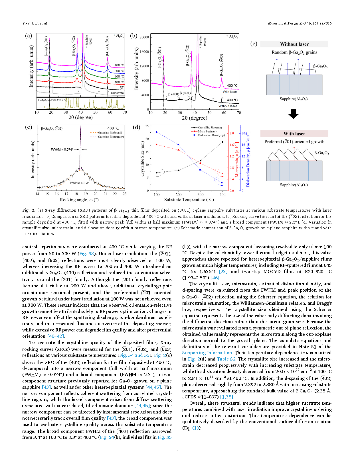
Orientation-selective growth mechanism: RF power control experiments confirmed that increasing RF power alone could not reproduce the (-201) orientation-selective growth achieved under laser irradiation, indicating that laser assistance provides additional pulsed energy for surface migration and atomic rearrangement.
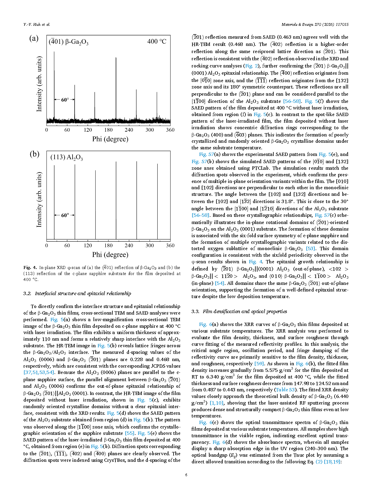
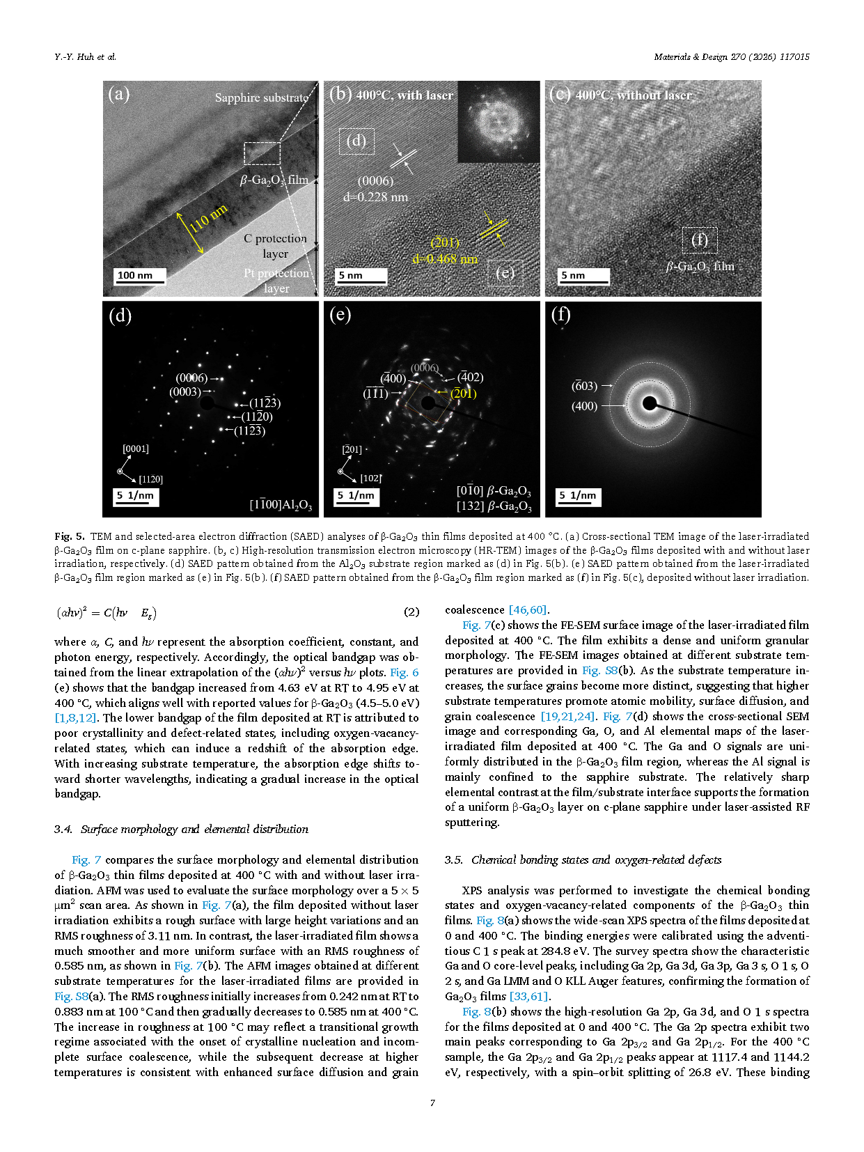
Full clarification of film-substrate epitaxial relationship:Combined characterizations including XRD, reciprocal space mapping, φ-scan, HR-TEM and SAED verify β-Ga₂O₃ (-201) || Al₂O₃ (0001) epitaxy and six equivalent in-plane rotational domains inside films.
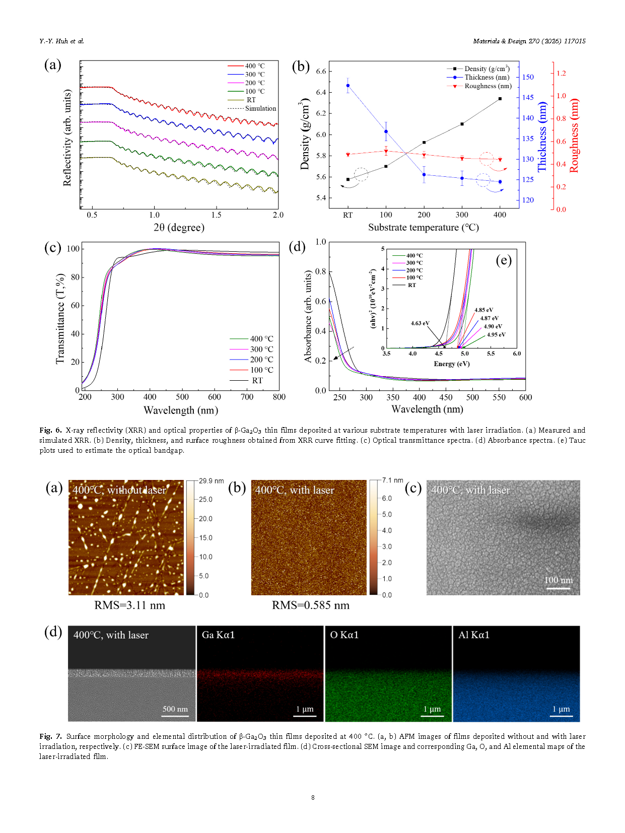
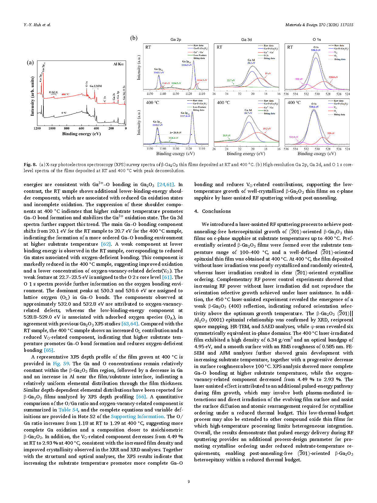
Excellent comprehensive film performance: Films grown at 400 ℃ reach density of 6.34 g/cm³ and optical bandgap of 4.95 eV. The RMS (Root-Mean-Square) roughness is 0.585 nm (from surface morphology characterization, Fig.7(b)). XPS proves strengthened Ga-O bonding and reduced oxygen-vacancy-related defects at elevated substrate temperature.
Potential for further extension:This low‑thermal‑budget strategy can be extended to other compound‑oxide thin‑film systems limited by high‑temperature processing.
Conclusion
We introduced a laser‑assisted RF sputtering process to achieve post‑annealing‑free heteroepitaxial growth of (-201)‑oriented β-Ga₂O₃ thin films on c‑plane sapphire at substrate temperatures up to 400 ℃. Preferentially oriented β-Ga₂O₃ films were formed over the substrate temperature range of 100–400 ℃, and a well‑defined (-201)‑oriented epitaxial thin film was obtained at 400 ℃. At 400 ℃, the film deposited without laser irradiation was poorly crystallized and randomly oriented, whereas laser irradiation resulted in clear (201)‑oriented crystalline ordering. Complementary RF power control experiments showed that increasing RF power without laser irradiation did not reproduce the orientation selective growth achieved under laser assistance. In addition, the 450 ℃ laser‑assisted experiment revealed the emergence of a weak β-Ga₂O₃ (400) reflection, indicating reduced orientation selectivity above the optimum growth temperature. The β-Ga₂O₃ (-201)|| Al₂O₃ (0001) epitaxial relationship was confirmed by XRD, reciprocal space mapping, HR‑TEM, and SAED analyses, while φ‑scan revealed six symmetrically equivalent in‑plane domains. The 400 ◦C laser‑irradiated film exhibited a high density of 6.34 g/cm³ and an optical bandgap of 4.95 eV, and a smooth surface with an RMS roughness of 0.585 nm. FE‑SEM and AFM analyses further showed grain development with increasing substrate temperature, together with a progressive decrease in surface roughness above 100 ℃ XPS analysis showed more complete Ga–O bonding at higher substrate temperatures, while the oxygen‑vacancy‑related component decreased from 4.49 % to 2.93 %. The laser‑assisted effect is attributed to an additional pulsed‑energy pathway during film growth, which may involve both plasma‑mediated interactions and direct irradiation of the evolving film surface and assist the surface diffusion and atomic rearrangement required for crystalline ordering under a reduced thermal budget. This low‑thermal‑budget process may also be extended to other compound oxide thin films for which high‑temperature processing limits heterogeneous integration. Overall, the results demonstrate that pulsed energy delivery during RF sputtering provides an additional process‑design parameter for promoting crystalline ordering under reduced substrate‑temperature requirements, enabling post‑annealing‑free (-201)‑oriented β‑Ga₂O₃ heteroepitaxy within a reduced thermal budget.
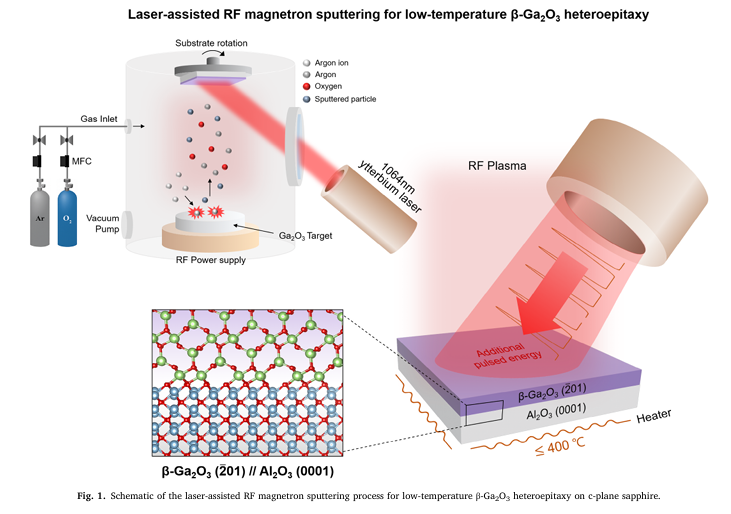
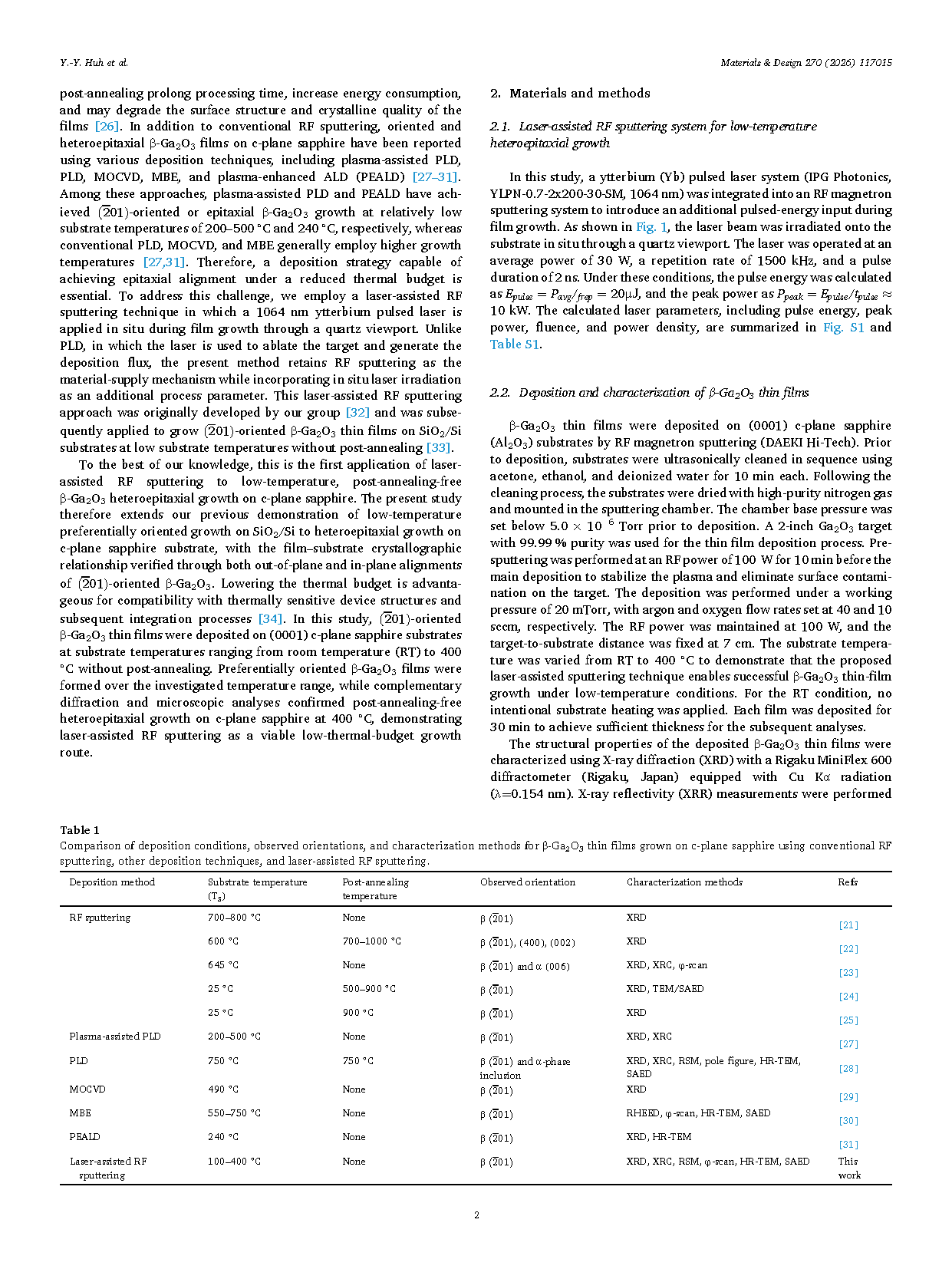
Fig. 1. Schematic of the laser-assisted RF magnetron sputtering process for low-temperature β-Ga₂O₃ heteroepitaxy on c-plane sapphire.
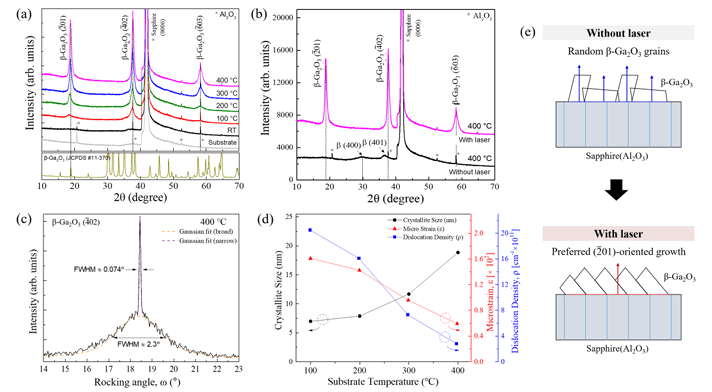
Fig. 2. (a) X-ray diffraction (XRD) patterns of β‑Ga₂O₃ thin films deposited on (0001) c-plane sapphire substrates at various substrate temperatures with laser irradiation. (b) Comparison of XRD patterns for films deposited at 400 ◦C with and without laser irradiation. (c) Rocking curve (ω-scan) of the (-402) reflection for the sample deposited at 400 °C, fitted with narrow peak (full width at half maximum (FWHM) ≈ 0.074°) and a broad component (FWHM ≈2.3°). (d) Variation in crystallite size, microstrain, and dislocation density with substrate temperature. (e) Schematic comparison of β-Ga₂O₃ growth on c-plane sapphire without and with laser irradiation.
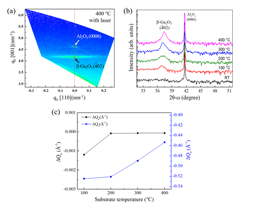
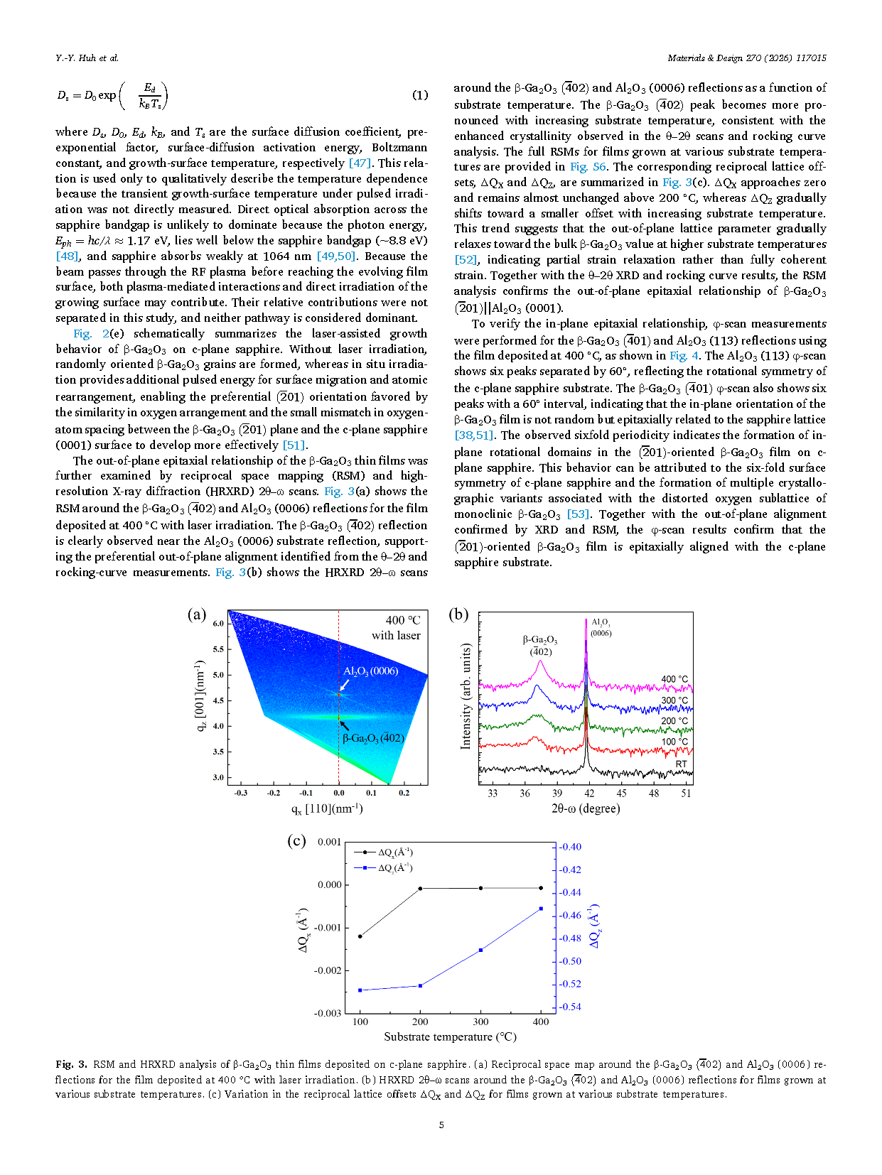
Fig. 3. RSM and HRXRD analysis of β‑Ga₂O₃ thin films deposited on c‑plane sapphire. (a) Reciprocal space map around the β‑Ga₂O₃ (-402) and Al₂O₃ (0006) reflections for the film deposited at 400 °C with laser irradiation. (b) HRXRD 2θ‑ω scans around the β‑Ga₂O₃ (-402) and Al₂O₃ (0006) reflections for films grown at various substrate temperatures. (c) Variation in the reciprocal lattice offsets ΔQₓ and ΔQz for films grown at various substrate temperatures.
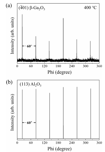
Fig. 4. In-plane XRD φ-scan of (a) the (-401) reflection of β-Ga₂O₃ and (b) the (113) reflection of the c-plane sapphire substrate for the film deposited at 400 °C.
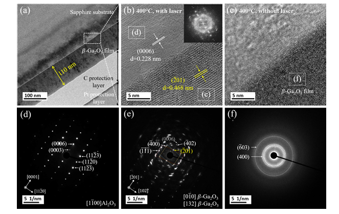
Fig. 5. TEM and selected-area electron diffraction (SAED) analyses of β-Ga₂O₃ thin films deposited at 400°C. (a) Cross-sectional TEM image of the laser-irradiated β-Ga₂O₃ film on c-plane sapphire. (b, c) High-resolution transmission electron microscopy (HR-TEM) images of the β-Ga₂O₃ films deposited with and without laser irradiation, respectively. (d) SAED pattern obtained from the Al₂O₃ substrate region marked as (d) in Fig. 5 (b).(e) SAED pattern obtained from the laser-irradiated β-Ga₂O₃ film region marked as (e) in Fig. 5 (b).(f) SAED pattern obtained from the β-Ga₂O₃ film region marked as (f) in Fig. 5 (c), deposited without laser irradiation.
DOI:
doi.org/10.1016/j.matdes.2026.117015
Instruction
Official Account

Cooperation
Top
