


Researchers from The Hong Kong University of Science and Technology (Guangzhou) have published a dissertation titled " Epitaxial β-Ga₂O₃ with tailored UV response for high-performance and stable perovskite solar cells " in Applied Physics Reviews.
Background
The long-term stability of perovskite solar cells (PSCs) remains a critical challenge for practical application. Among various environ mental stressors, ultraviolet (UV) irradiation is particularly detrimental. High-energy UV photons can activate defect states, accelerate ion migration, and induce chemical degradation in the perovskite layer and charge-transport interfaces. Such degradation is commonly accompanied by irreversible photocurrent loss and a decline in power conversion efficiency. Effective UV protection should therefore reduce the incident UV photon flux before it reaches the perovskite absorber and its charge-transport interfaces.
Abstract
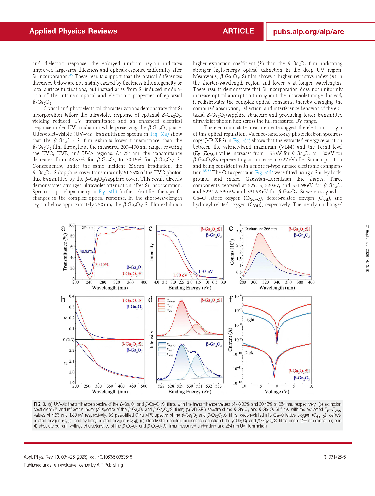
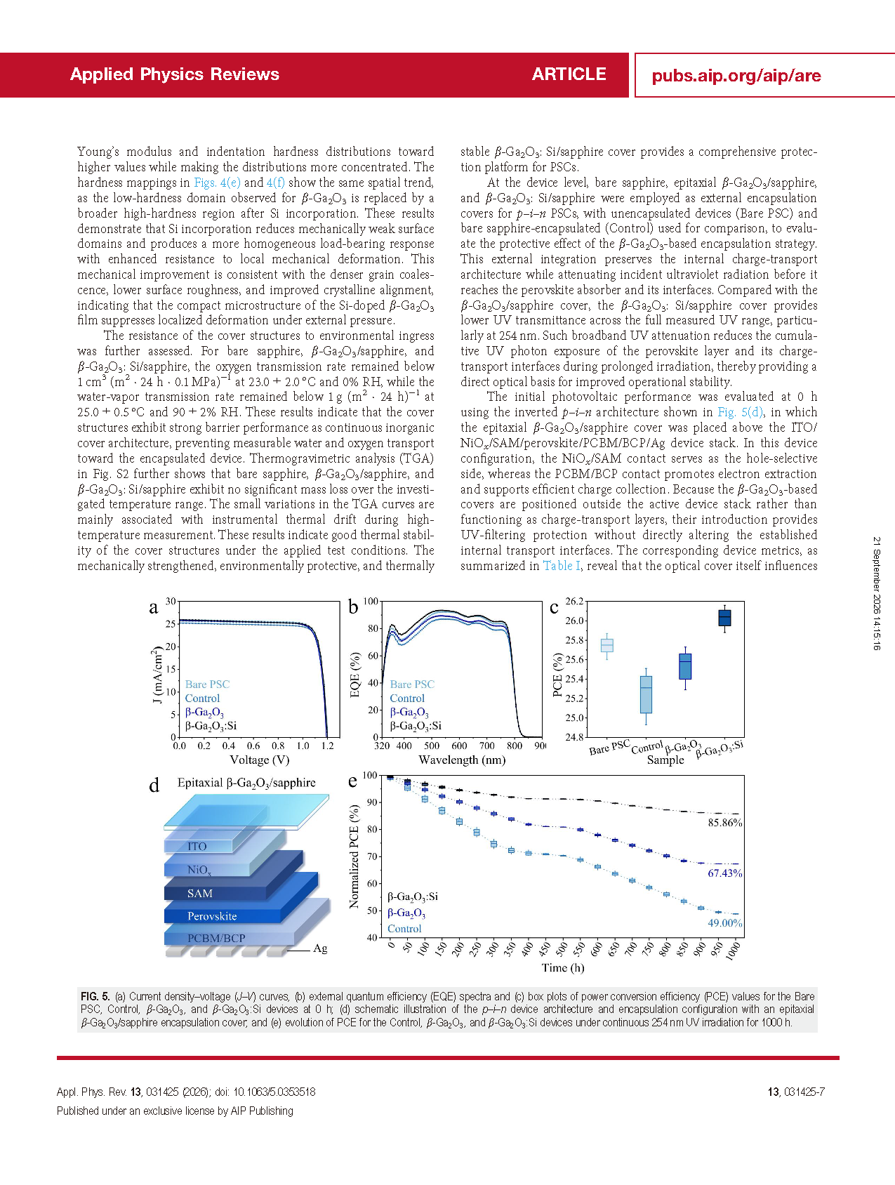
Ultraviolet exposure accelerates degradation of perovskite absorbers and charge-transport interfaces, whereas internal ultraviolet-protection layers can complicate fabrication and affect charge extraction. Here, Si-doped epitaxial β-Ga₂O₃ (β-Ga₂O₃: Si) films were grown on sapphire by metal–organic chemical vapor deposition and used as external encapsulation covers for inverted p–i–n perovskite solar cells. Si incorporation preserves the monoclinic β-Ga₂O₃ phase and comparable film thickness, while promoting grain coalescence, reducing surface roughness, and improving large-area optical uniformity. More importantly, it tailors the ultraviolet response of the β-Ga₂O₃: Si/sapphire structure, lowering transmittance across the 200–400 nm range, with the value at 254 nm decreasing from 48.83% to 30.15%. The altered ultraviolet transmission is accompanied by redistributed optical constants, a modified surface electronic configuration, a more lattice oxygen dominated surface environment, and enhanced 254 nm ultraviolet photoresponse. The β-Ga₂O₃:Si/sapphire cover also shows uniform surface mechanical response, effective environmental barrier performance, and thermal stability. Perovskite solar cells employing this cover deliver an initial power conversion efficiency of 26.16% and retain 85.86% of their initial efficiency after 1000 h of continuous 254 nm irradiation, compared with 49.00% for bare-sapphire-encapsulated controls. These results establish β-Ga₂O₃: Si/sapphire as a multifunctional external cover for ultraviolet spectral management and durable operation of perovskite solar cells.
Conclusion
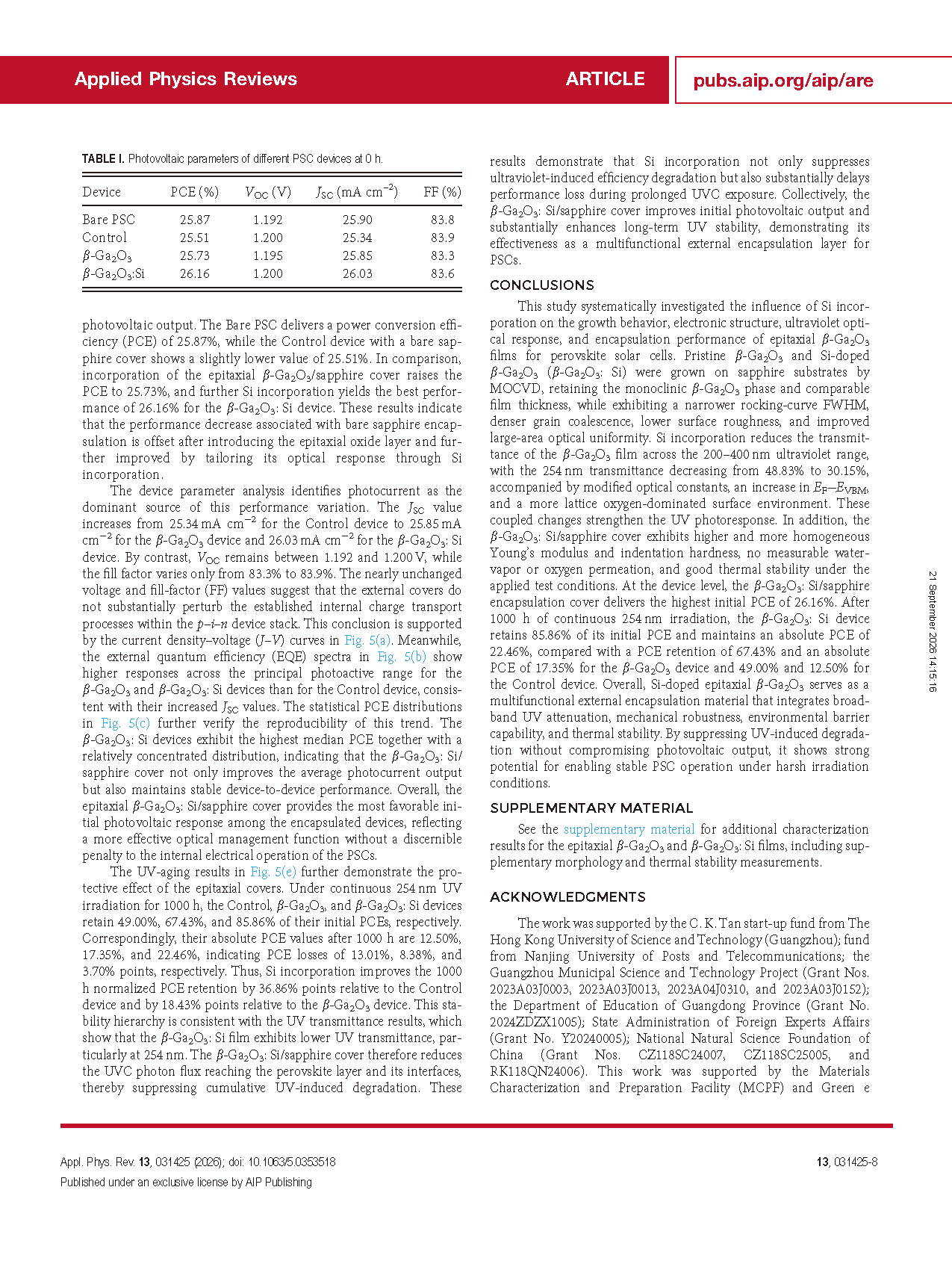
This study systematically investigated the influence of Si incorporation on the growth behavior, electronic structure, ultraviolet optical response, and encapsulation performance of epitaxial β-Ga₂O₃ films for perovskite solar cells. Pristine β-Ga₂O₃ and Si-doped β-Ga₂O₃ (β-Ga₂O₃: Si) were grown on sapphire substrates by MOCVD, retaining the monoclinic β-Ga₂O₃ phase and comparable film thickness, while exhibiting a narrower rocking-curve FWHM, denser grain coalescence, lower surface roughness, and improved large-area optical uniformity. Si incorporation reduces the transmittance of the β-Ga₂O₃ film across the 200–400nm ultraviolet range, with the 254nm transmittance decreasing from 48.83% to 30.15%, accompanied by modified optical constants, an increase in EF−EVBM, and a more lattice oxygen-dominated surface environment. These coupled changes strengthen the UV photoresponse. In addition, the β-Ga₂O₃: Si/sapphire cover exhibits higher and more homogeneous Young’s modulus and indentation hardness, no measurable water- vapor or oxygen permeation, and good thermal stability under the applied test conditions. At the device level, the β-Ga₂O₃: Si/sapphire encapsulation cover delivers the highest initial PCE of 26.16%. After 1000 h of continuous 254nm irradiation, the β-Ga₂O₃: Si device retains 85.86% of its initial PCE and maintains an absolute PCE of 22.46%, compared with a PCE retention of 67.43% and an absolute PCE of 17.35% for the β-Ga₂O₃ device and 49.00% and 12.50% for the Control device. Overall, Si-doped epitaxial β-Ga₂O₃ serves as a multifunctional external encapsulation material that integrates broad band UV attenuation, mechanical robustness, environmental barrier capability, and thermal stability. By suppressing UV-induced degradation without compromising photovoltaic output, it shows strong potential for enabling stable PSC operation under harsh irradiation conditions.
Project Support
The work was supported by the C. K. Tan start-up fund from The Hong Kong University of Science and Technology (Guangzhou); fund from Nanjing University of Posts and Telecommunications; the Guangzhou Municipal Science and Technology Project (Grant Nos. 2023A03J0003, 2023A03J0013, 2023A04J0310, and 2023A03J0152); the Department of Education of Guangdong Province (Grant No. 2024ZDZX1005); State Administration of Foreign Experts Affairs (Grant No. Y20240005); National Natural Science Foundation of China (Grant Nos. CZ118SC24007, CZ118SC25005, and RK118QN24006). This work was supported by the Materials Characterization and Preparation Facility (MCPF) and Green e Materials (GeM) Laboratory at the Hong Kong University of Science and Technology (Guangzhou). The material growth in this paper was performed using equipment from Guangzhou Tanoxi Company.

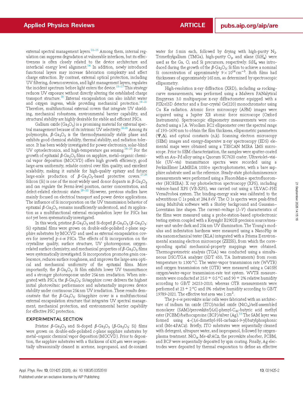
FIG. 1. (a) Thickness distributions of the β-Ga₂O₃ and β-Ga₂O₃:Si films measured by spectroscopic ellipsometry, showing mean values of 164.44nm for β-Ga₂O₃ and 165.89nm for β-Ga₂O₃:Si; (b) XRD patterns of the β-Ga₂O₃ and β-Ga₂O₃:Si films grown on sapphire substrates; (c) x rocking curves measured around the β-Ga₂O₃ (201) reflection for the β-Ga₂O₃ and β-Ga₂O₃:Si films, with the corresponding FWHM values; (d) and (i) low-magnification SEM images of the β-Ga₂O₃ and β-Ga₂O₃:Si films, respectively; (e) and (g) magnified SEM images of the boxed regions in (d) and (i), respectively; (f) and (h) corresponding binarized SEM images; (j) and (k) EDS elemental maps of Ga and O for the β-Ga₂O₃ film; and (l) and (m) EDS elemental maps of Ga and O for the β-Ga₂O₃:Si film.
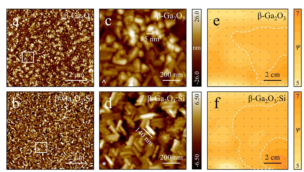
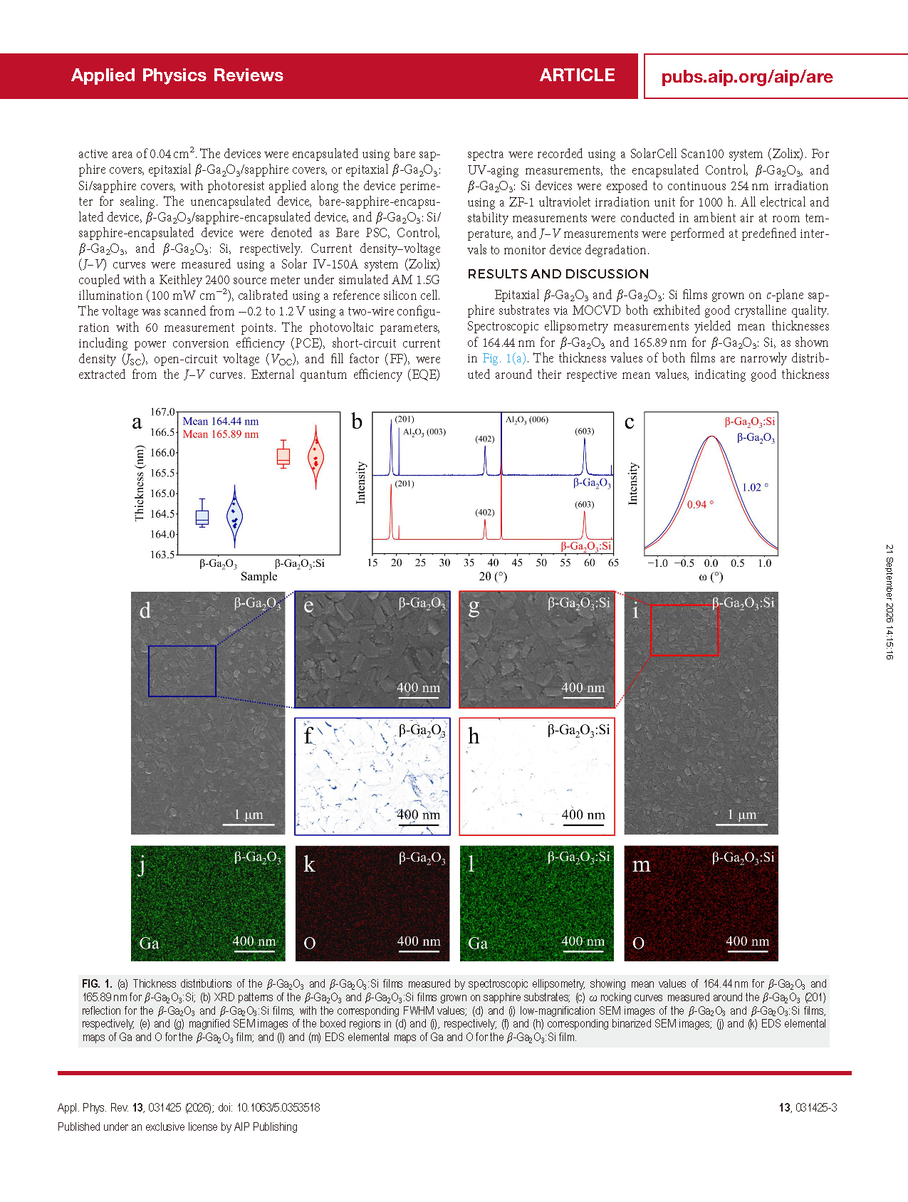
FIG. 2. (a) and (b) Low-magnification AFM topography images of the β-Ga₂O₃ and β-Ga₂O₃:Si films, respectively, with RMS roughness values of 8.622 and 2.528nm; (c) and (d) magnified AFM images of the boxed regions in (a) and (b), respectively, with representative grain dimensions indicated; and (e) and (f) spatial mappings of the ellipsometric parameter W for the β-Ga₂O₃ and β-Ga₂O₃:Si films, respectively, where white dashed contours indicate uniform W regions.
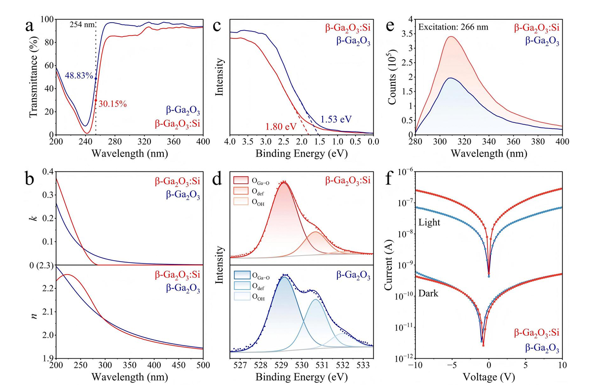
FIG. 3. (a) UV–vis transmittance spectra of the β-Ga₂O₃ and β-Ga₂O₃:Si films, with the transmittance values of 48.83% and 30.15% at 254nm, respectively; (b) extinction coefficient (k) and refractive index (n) spectra of the β-Ga₂O₃ and β-Ga₂O₃:Si films; (c) VB-XPS spectra of the β-Ga₂O₃ and β-Ga₂O₃:Si films, with the extracted EF−EVBM values of 1.53 and 1.80 eV, respectively; (d) peak-fitted O 1s XPS spectra of the β-Ga₂O₃ and β-Ga₂O₃:Si films, deconvoluted into Ga–O lattice oxygen (OGa−O), defect- related oxygen (Odef), and hydroxyl-related oxygen (OOH); (e) steady-state photoluminescence spectra of the β-Ga₂O₃ and β-Ga₂O₃:Si films under 266nm excitation; and (f) absolute current–voltage characteristics of the β-Ga₂O₃ and β-Ga₂O₃:Si films measured under dark and 254nm UV illumination.
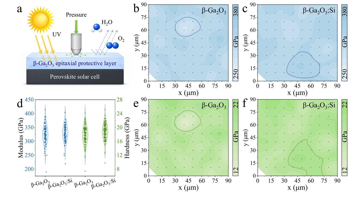
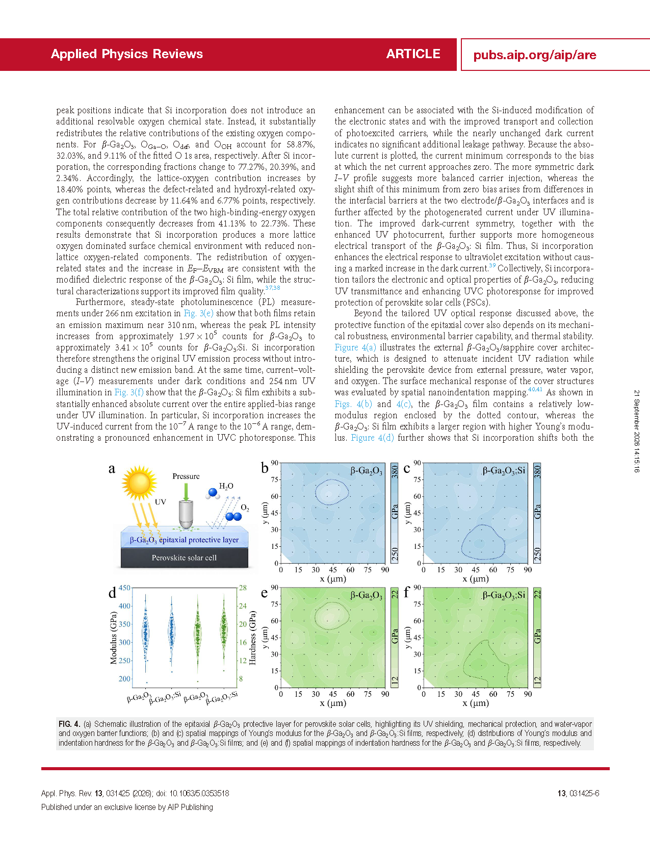
FIG. 4. (a) Schematic illustration of the epitaxial β-Ga₂O₃ protective layer for perovskite solar cells, highlighting its UV shielding, mechanical protection, and water-vapor and oxygen barrier functions; (b) and (c) spatial mappings of Young’s modulus for the β-Ga₂O₃ and β-Ga₂O₃:Si films, respectively; (d) distributions of Young’s modulus and indentation hardness for the β-Ga₂O₃ and β-Ga₂O₃:Si films; and (e) and (f) spatial mappings of indentation hardness for the β-Ga₂O₃ and β-Ga₂O₃:Si films, respectively.
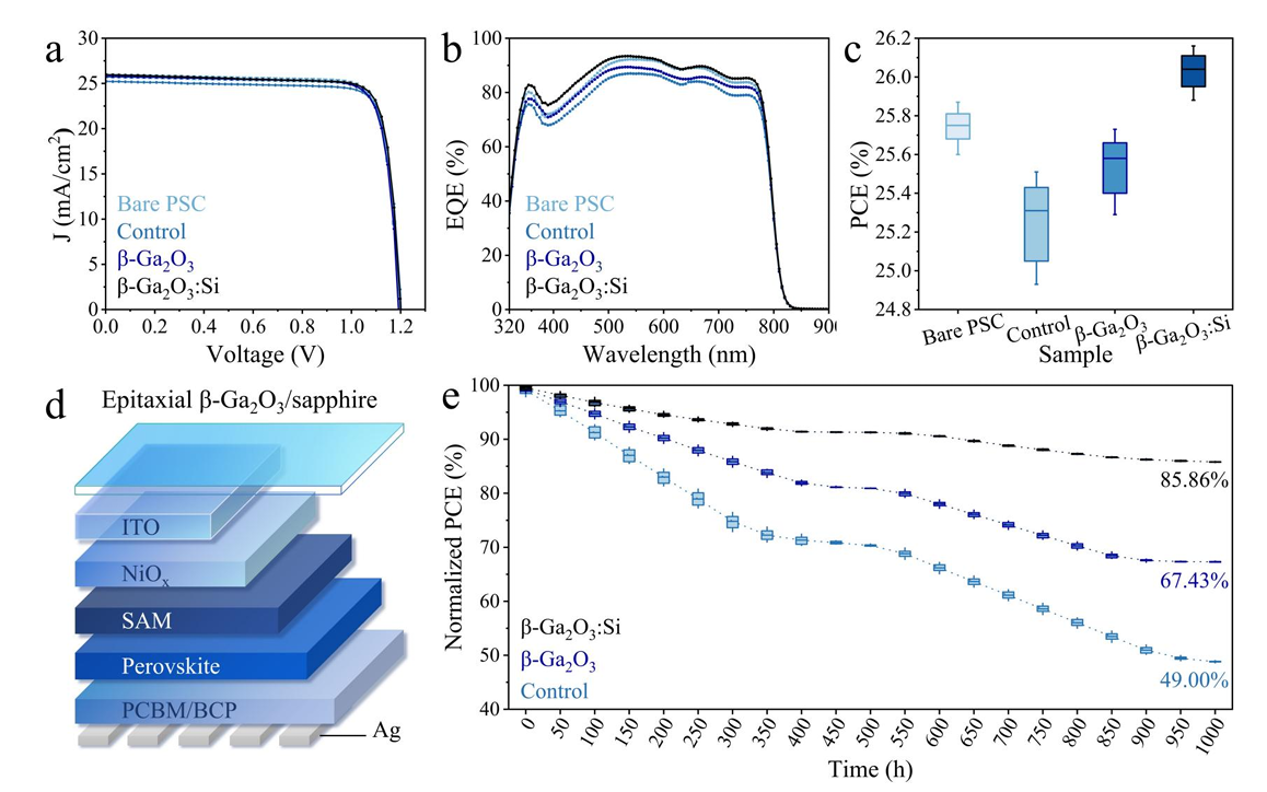
FIG. 5. (a) Current density–voltage (J–V) curves, (b) external quantum efficiency (EQE) spectra and (c) box plots of power conversion efficiency (PCE) values for the Bare PSC, Control, β-Ga₂O₃, and β-Ga₂O₃:Si devices at 0 h; (d) schematic illustration of the p–i–n device architecture and encapsulation configuration with an epitaxial β-Ga₂O₃/sapphire encapsulation cover; and (e) evolution of PCE for the Control, β-Ga₂O₃, and β-Ga₂O₃:Si devices under continuous 254nm UV irradiation for 1000 h.
DOI:
doi.org/10.1063/5.0353518
Instruction
Official Account

Cooperation
Top
