


Researchers from Texas State University have published a dissertation titled " Epitaxial growth and characterization of hexagonal ε-(InₓGa₁₋ₓ)₂O₃ (x=0.05 and 0.15) on AlN " in Journal of Physics D: Applied Physics.
Background
In high-power and harsh-condition-compatible electronics, Ga₂O₃ has emerged as a prominent successor to GaN and SiC, having an ultra-wide bandgap (UWBG) of 4.8 eV and an excellent breakdown voltage of 8 MV cm⁻¹. Among the six polymorphs of Ga₂O₃ (α, β, γ, δ, ε, and κ), hexagonal ε- Ga₂O₃ has garnered significant attention due to its highly symmetric and isotropic hexagonal crystal structure. Additionally, ε-(InₓGa₁₋ₓ)₂O₃ allows bandgap tuning from 4.9 eV–2.9 eV with indium content variation, an important requirement for high-power optoelectronics. However, a fundamental limitation of all Ga₂O₃ derivatives is their relatively low thermal conductivity (~27 W m⁻¹ K⁻¹), posing significant challenges for high-power device applications. This issue can be mitigated by introducing another UWBG material with higher thermal conductivity to form a heterojunction. AlN, with an UWBG of 6.2 eV and a relatively high thermal conductivity (321 W m⁻¹ K⁻¹), can work as a heat spreader. Additionally, the lattice mismatch between ε- Ga₂O₃ and AlN is relatively low at 6.4%, compared with ~24.2% between ε-Ga₂O₃ and Si. Therefore, AlN can be introduced as a lattice-matching layer between ε-(InₓGa₁₋ₓ)₂O₃ and Si. While hexagonal ε-Ga₂O₃ and orthorhombic κ-Ga₂O₃ growth on III-nitrides has been explored to some extent, the exploration of hexagonal ε-(InₓGa₁₋ₓ)₂O₃ growth on AlN and ε-(InₓGa₁₋ₓ)₂O₃ growth using PLD was yet to be attempted. PLD does not require gas-based complex chemistry or expensive gas systems and allows highly accurate stoichiometric transfer of compounds.
Abstract
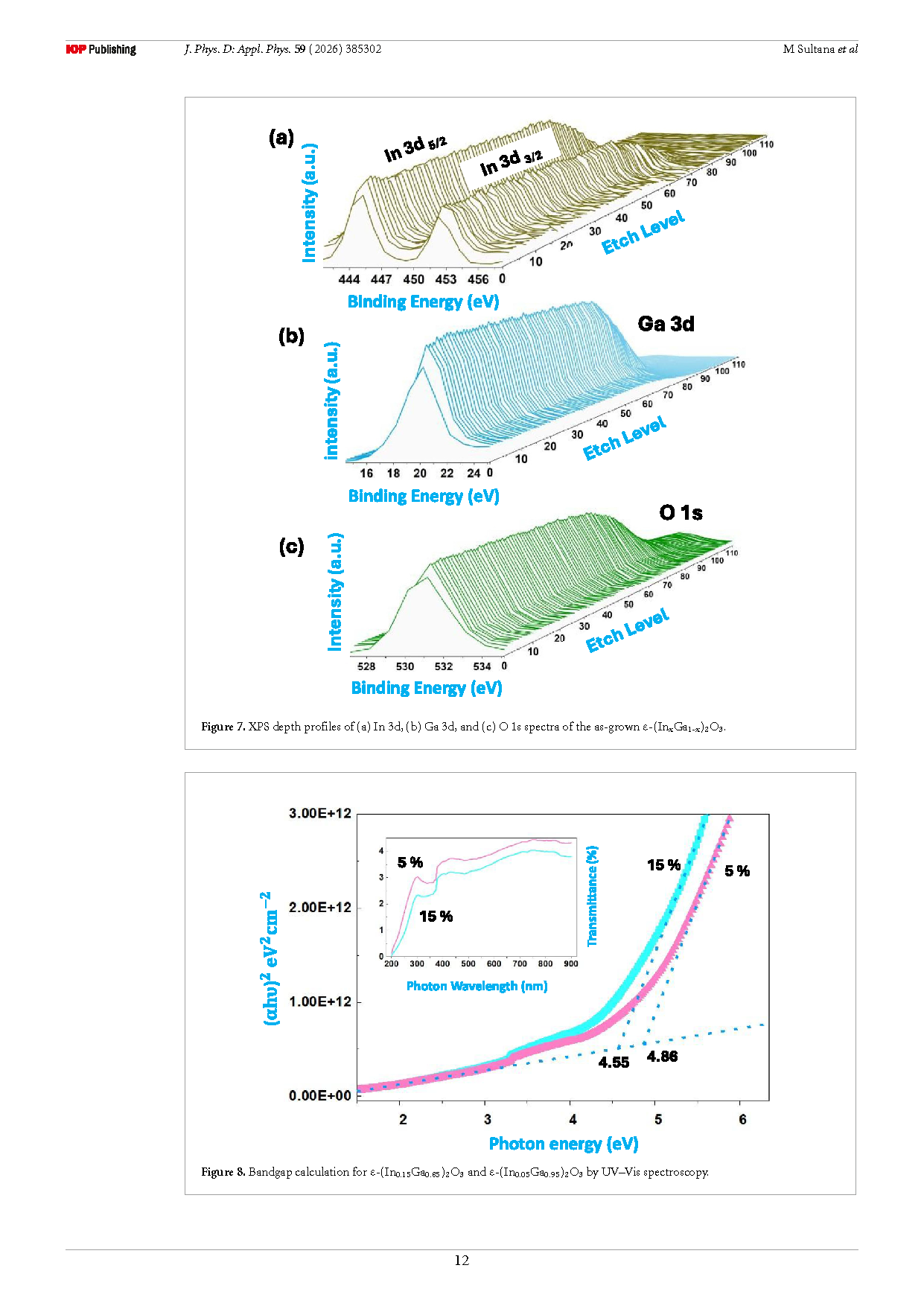
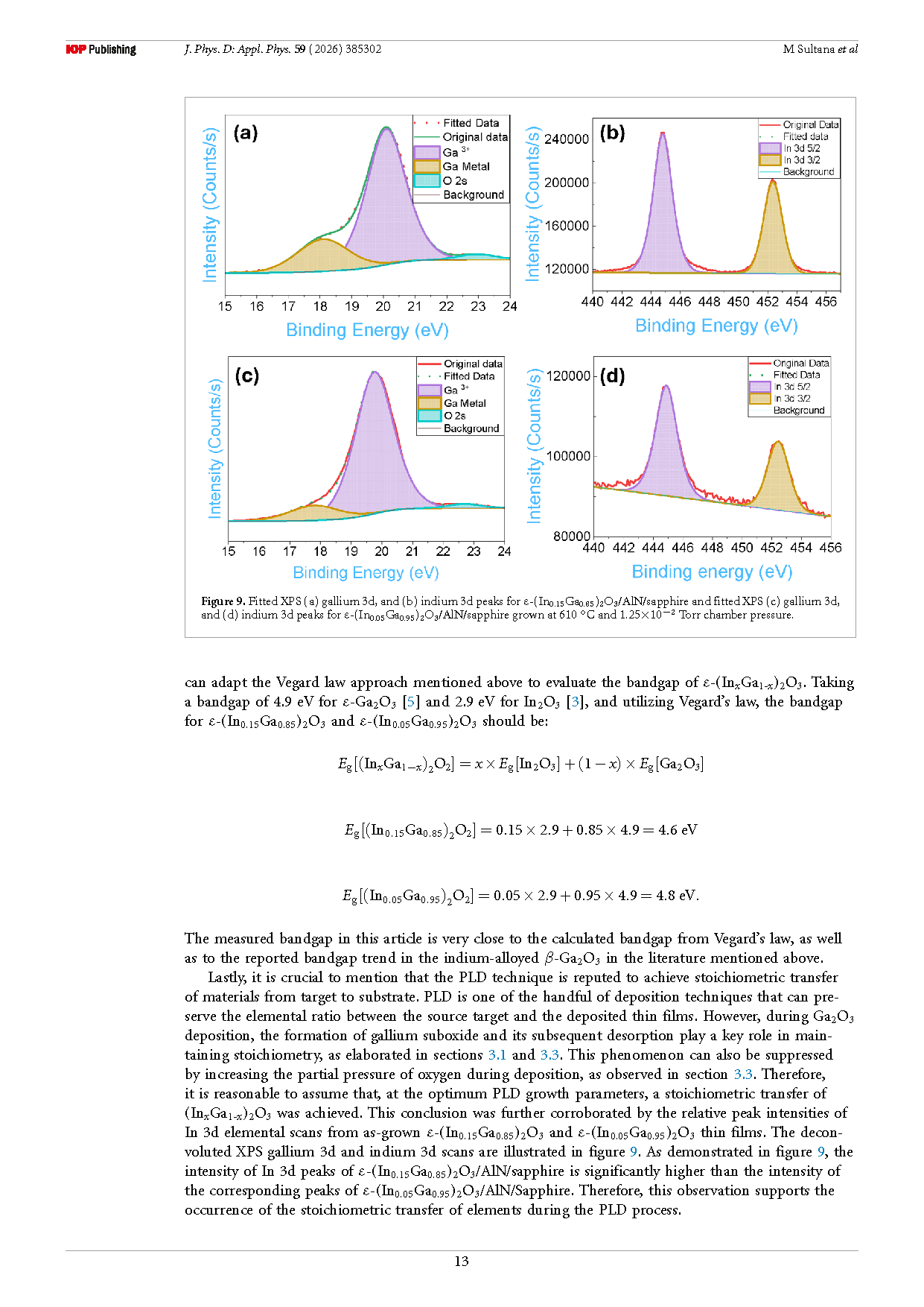
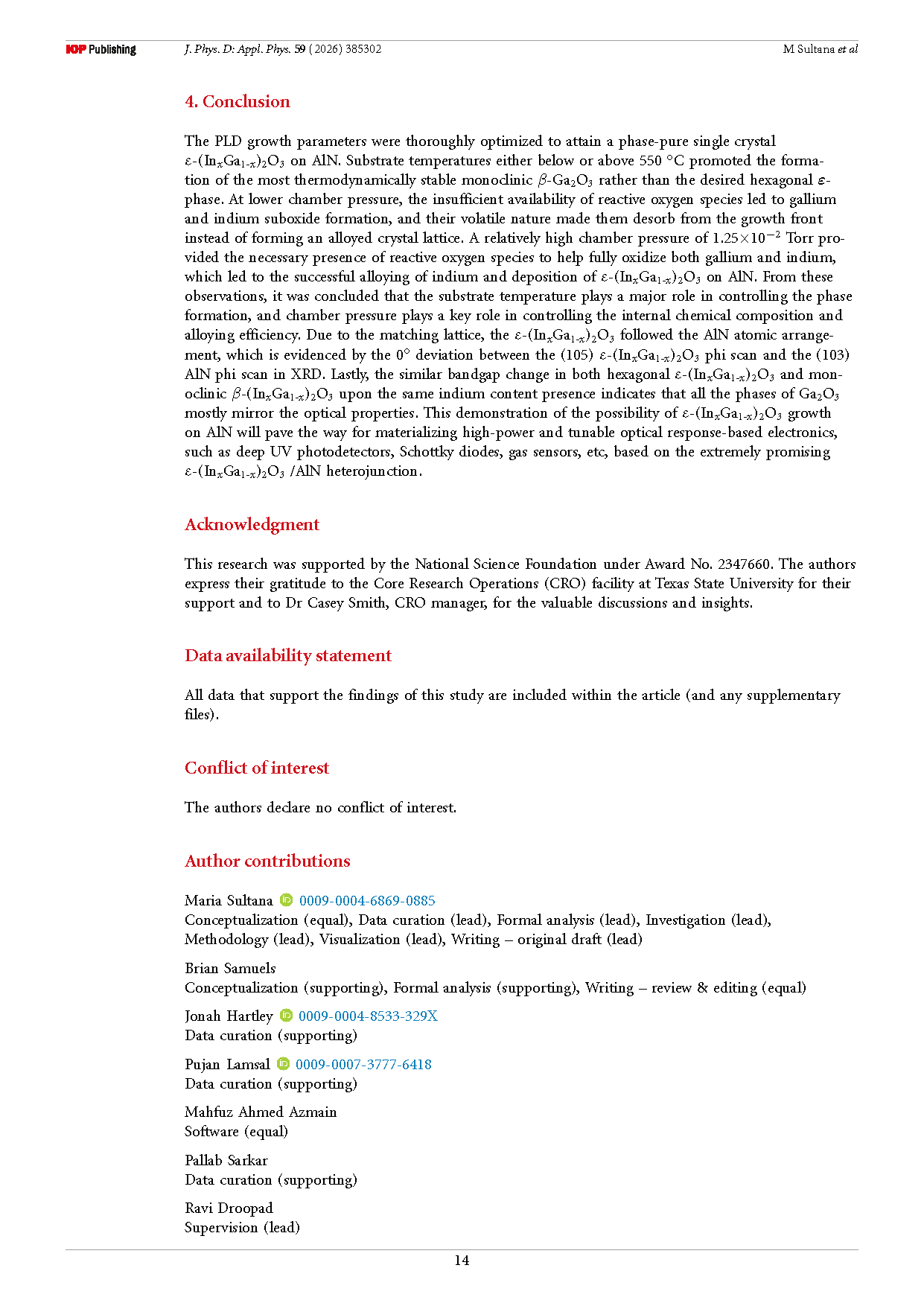
Growth parameter optimization to deposit hexagonal ε-(InₓGa₁₋ₓ)₂O₃ (x=0.05 and 0.15) on AlN by pulsed laser deposition (PLD) was performed for the first time. The PLD heater temperature and chamber oxygen pressure were systematically tuned to fine‑tune the optimum growth parameters of ε-(InₓGa₁₋ₓ)₂O₃ on AlN. A heater temperature of 550 °C was the most suitable temperature to obtain the metastable hexagonal phase, avoiding polycrystallinity, suppressing the formation of cubic indium oxide, and inhibiting transformation to the monoclinic β‑Ga₂O₃ phase. A chamber pressure of 1.25×10⁻² Torr was necessary to uniformly incorporate indium throughout the ε‑Ga₂O₃ lattice and turn it into ε-(InₓGa₁₋ₓ)₂O₃. The X‑ray diffraction (XRD) phi scans confirmed the hexagonal phase, and the epitaxial relationship was determined to be (105) ε-(InₓGa₁₋ₓ)₂O₃ ∥ (103) AlN. The presence of indium in the ε‑Ga₂O₃ was confirmed by XRD 2θ peak position shift and X‑ray photoelectron spectroscopy (XPS) via the elemental scan depth profile, with a minor presence of unoxidized gallium atoms and oxygen vacancy centers. The measured bandgaps were 4.55 eV and 4.86 eV for ε‑(In₀.₁₅Ga₀.₈₅)₂O₃ and ε‑(In₀.₀₅Ga₀.₉₅)₂O₃, respectively.
Highlights
First-time PLD epitaxy of ε-(InₓGa₁₋ₓ)₂O₃ on AlN: The team successfully deposited hexagonal ε-(InₓGa₁₋ₓ)₂O₃ (x=0.05 and 0.15) on AlN by pulsed laser deposition (PLD) for the first time, filling the research gap in ε-(InₓGa₁₋ₓ)₂O₃ growth on AlN via PLD.
Temperature optimization window: Determined 550 °C as the optimal heater temperature to obtain phase-pure single-crystal ε phase, avoiding polycrystallinity, suppressing cubic In₂O₃ formation and β-Ga₂O₃ transformation, highlighting the temperature sensitivity of ε phase growth.
Pressure-controlled doping: A chamber pressure of 1.25×10⁻² Torr was determined to ensure uniform indium incorporation into the ε-Ga₂O₃ lattice to form ε-(InₓGa₁₋ₓ)₂O₃.
Phase identification and epitaxial relationship: Confirmed the hexagonal ε phase (distinct from orthorhombic κ phase) via XRD phi scans, with the epitaxial relationship (105) ε-(InₓGa₁₋ₓ)₂O₃∥(103) AlN.
Composition-tunable bandgap: XRD 2θ peak shift combined with XPS depth profile confirmed uniform indium incorporation; bandgaps of 4.55 eV and 4.86 eV were measured for ε-(In₀.₁₅Ga₀.₈₅)₂O₃ and ε-(In₀.₀₅Ga₀.₉₅)₂O₃, respectively, demonstrating bandgap tunability with indium content.
Conclusion
The PLD growth parameters were thoroughly optimized to attain a phase‑pure single crystal ε-(InₓGa₁₋ₓ)₂O₃ on AlN. Substrate temperatures either below or above 550 °C promoted the formation of the most thermodynamically stable monoclinic β‑Ga₂O₃ rather than the desired hexagonal ε phase. At lower chamber pressure, the insufficient availability of reactive oxygen species led to gallium and indium suboxide formation, and their volatile nature made them desorb from the growth front instead of forming an alloyed crystal lattice. A relatively high chamber pressure of 1.25×10⁻² Torr provided the necessary presence of reactive oxygen species to help fully oxidize both gallium and indium, which led to the successful alloying of indium and deposition of ε-(InₓGa₁₋ₓ)₂O₃ on AlN. From these observations, it was concluded that the substrate temperature plays a major role in controlling the phase formation, and chamber pressure plays a key role in controlling the internal chemical composition and alloying efficiency. Due to the matching lattice, the ε-(InₓGa₁₋ₓ)₂O₃ followed the AlN atomic arrangement, which is evidenced by the 0° deviation between the (105) ε-(InₓGa₁₋ₓ)₂O₃ phi scan and the (103) AlN phi scan in XRD. Lastly, the similar bandgap change in both hexagonal ε-(InₓGa₁₋ₓ)₂O₃ and monoclinic β‑(InₓGa₁₋ₓ)₂O₃ upon the same indium content presence indicates that all the phases of Ga₂O₃ mostly mirror the optical properties. This demonstration of the possibility of ε-(InₓGa₁₋ₓ)₂O₃ growth on AlN will pave the way for materializing high‑power and tunable optical response‑based electronics, such as deep UV photodetectors, Schottky diodes, gas sensors, etc, based on the extremely promising ε-(InₓGa₁₋ₓ)₂O₃ /AlN heterojunction.
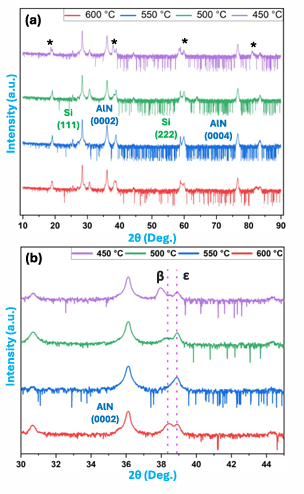
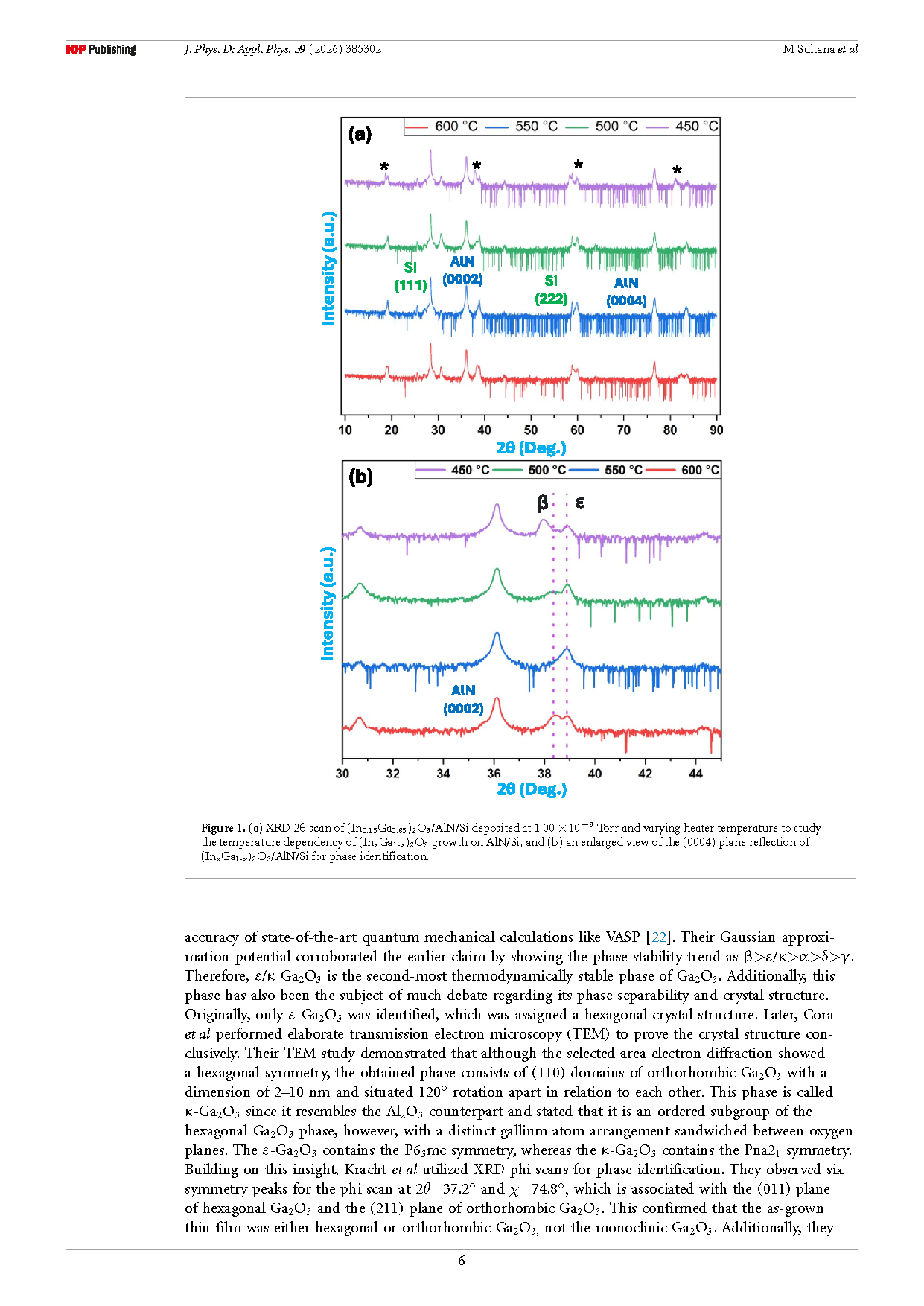
Fig 1. (a) XRD 2θ scan of (In₀.₁₅Ga₀.₈₅)₂O₃/AlN/Si deposited at 1.00×10⁻³ Torr and varying heater temperature to study the temperature dependency of (InₓGa₁₋ₓ)₂O₃ growth on AlN/Si, and (b) an enlarged view of the (0004) plane reflection of (InₓGa₁₋ₓ)₂O₃/AlN/Si for phase identification.
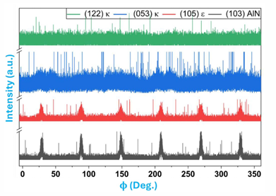
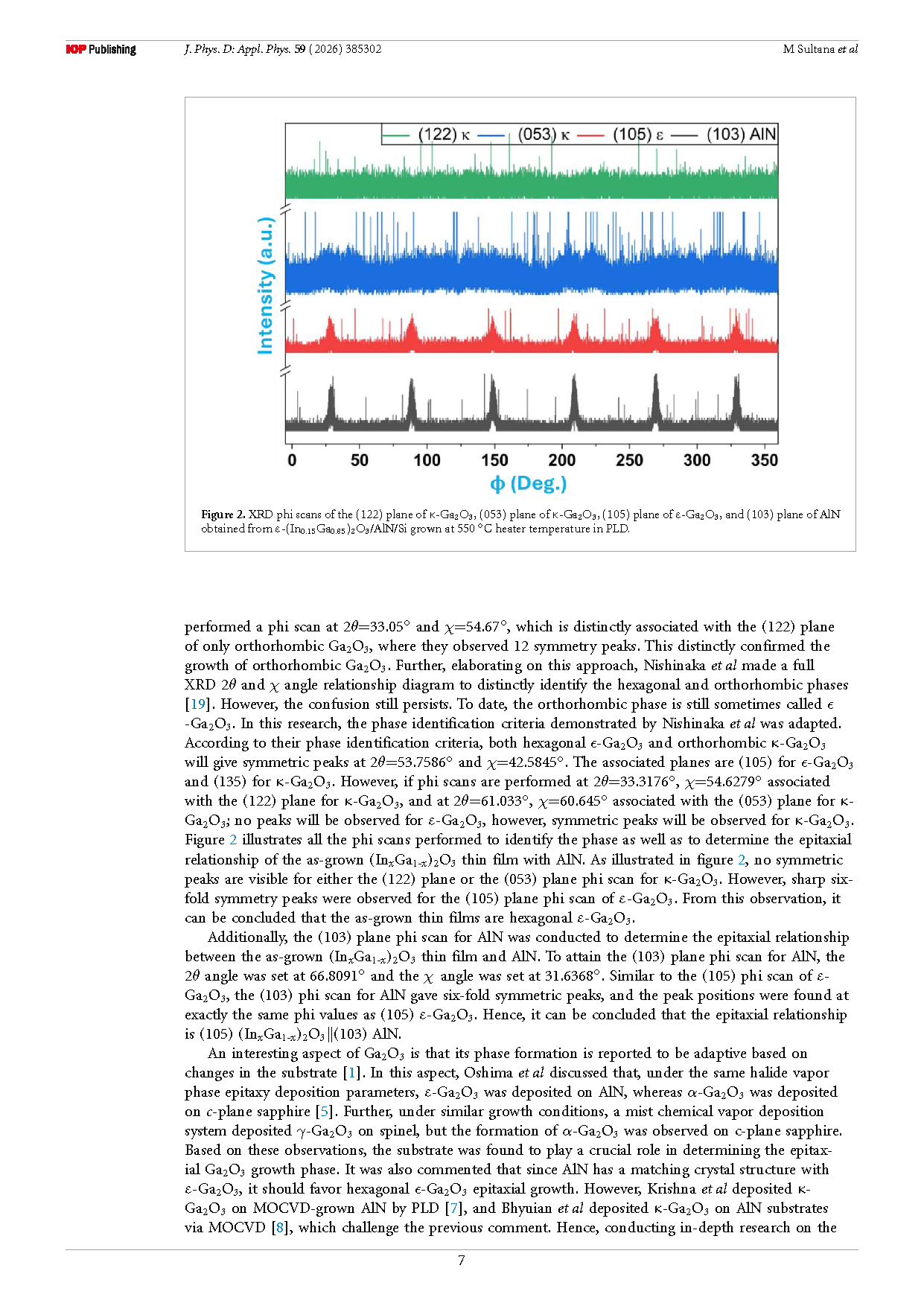
Fig 2. XRD phi scans of the (122) plane of κ‑Ga₂O₃, (053) plane of κ‑Ga₂O₃, (105) plane of ε‑Ga₂O₃, and (103) plane of AlN obtained from ε‑(In₀.₁₅Ga₀.₈₅)₂O₃/AlN/Si grown at 550 °C heater temperature in PLD.
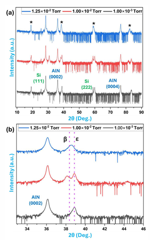
Fig 3. (a) XRD 2θ scan of ε‑(In₀.₁₅Ga₀.₈₅)₂O₃ deposited at 550 °C and varying chamber pressure to study the oxygen partial pressure dependency of ε‑(InₓGa₁₋ₓ)₂O₃ growth on AlN/Si, and (b) enlarged view of the (0004) plane reflection of ε‑(InₓGa₁₋ₓ)₂O₃ for indium infusion confirmation.
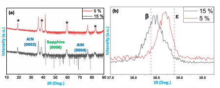
Fig 4. (a) XRD 2θ scan of ε-(InₓGa₁₋ₓ)₂O₃ grown at 1.25×10⁻² Torr chamber pressure with a change in indium content from 5% to 15%, and (b) enlarged view of the peak shift of the (0004) plane.
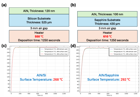
Fig 5. (a) AlN/Si and (b) AlN/sapphire template used for ε-(InₓGa₁₋ₓ)₂O₃ growth parameter optimization, surface temperature calculated from COMSOL simulations for (c) AlN/Si and (d) AlN/sapphire template.
DOI:
doi.org/10.1088/1361-6463/ae9d8e
Instruction
Official Account

Cooperation
Top
