


Researchers from the Shandong University and Qingdao University of Science and Technology have published a dissertation titled "Reconfiguring the Energy Relaxation Pathway via a Counterintuitive Defect Engineering for Synergistic Optimization of β-Ga₂O₃ Scintillators" in Laser & Photonics Reviews.
Background
High-efficiency, ultrafast scintillators were vital for CT, and Xray imaging, requiring both high light yield and rapid decay for superior resolution. Representative ultrafast scintillator materials like ZnO:Ga achieved 0.6–10 ns decay times; however, their minimal Stokes shift caused severe self-absorption, compromising light output and detection sensitivity. The trade-off between decay time and light yield has inevitably prompted research into novel scintillators characterized by ultrafast decay times.
Recently, β-Ga2O3 has attracted significant attention due to its excellent transmittance and the advantages of low-cost, large-scale fabrication. Crucially, β-Ga2O3 exhibited nanosecond-level emissions under radiation excitation. These properties made β-Ga2O3 an ideal candidate for ultra-fast scintillators. Excitingly, the emission energy of β-Ga2O3 was ∼1.5 eV lower than its bandgap. This property not only effectively suppressed the self-absorption but also provided an important basis for constructing a scintillator with both fast decay and high light yield.
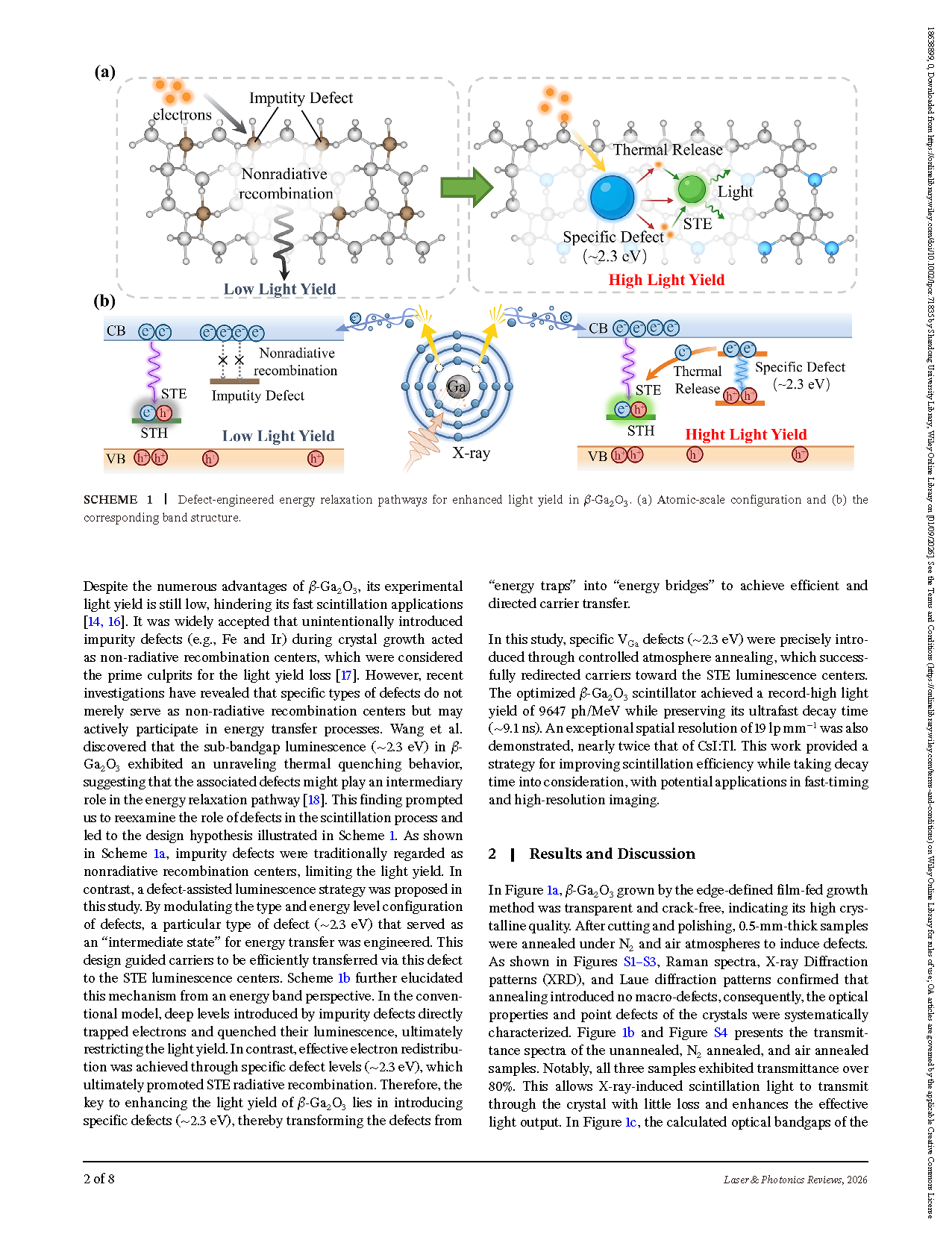
Despite the numerous advantages of β-Ga2O3, its experimental light yield is still low, hindering its fast scintillation applications. It was widely accepted that unintentionally introduced impurity defects (e.g., Fe and Ir) during crystal growth acted as non-radiative recombination centers, which were considered the prime culprits for the light yield loss. However, recent investigations have revealed that specific types of defects do not merely serve as non-radiative recombination centers but may actively participate in energy transfer processes. Wang et al. discovered that the sub-bandgap luminescence (∼2.3 eV) in β-Ga2O3 exhibited an unraveling thermal quenching behavior, suggesting that the associated defects might play an intermediary role in the energy relaxation pathway.
Abstract
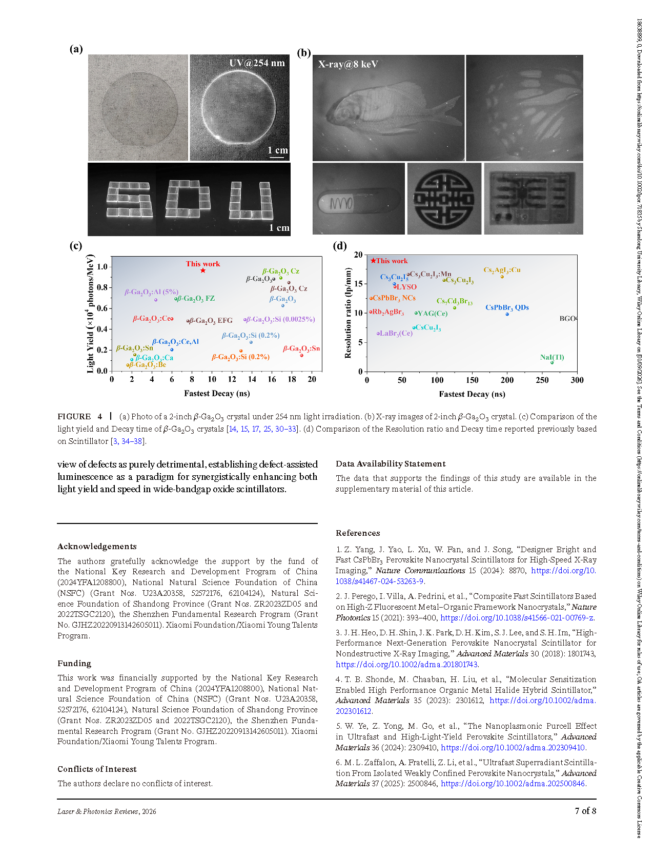
Scintillator development has long been constrained by the trade-off between decay time and light yield. Here, we reported a counterintuitive defect engineering strategy that successfully reconciles these conflicting metrics in β-Ga2O3. Through controlled atmosphere annealing, a specific configuration of gallium vacancies (VGa) is intentionally introduced which function as relay levels for energy transfer, effectively redirecting carriers toward self-trapped exciton (STE) luminescence channels. The optimized β-Ga2O3 scintillator achieves a high light yield of 9647 ph/MeV, representing a 1.38-fold enhancement over the unannealed crystal (6971 ph/MeV). Remarkably, this substantial improvement is attained while preserving the material's intrinsically ultrafast decay time (∼9.1 ns). Furthermore, the material demonstrates an outstanding spatial resolution of 19 lp mm−1, nearly twice that of the commercial benchmark CsI:Tl scintillator (∼10 lp mm−1). This work not only overturns the traditional perception of defects merely as non-radiative recombination centers but also establishes defect-assisted luminescence as a design principle for synergistically boosting the light yield and speed of wide-bandgap oxide scintillators.
Highlights
Proposes a counterintuitive defect engineering strategy that shifts focus from merely eliminating defects to actively modulating gallium vacancies (VGa) via air annealing, transforming defects from traditional "energy traps" into "energy relay stations" that facilitate carrier transport.
The optimized β-Ga₂O₃ achieves a light yield of 9647 ph/MeV, a 1.38-fold increase compared to the unannealed sample's 6971 ph/MeV, while maintaining an ultrafast decay time of approximately 9.1 ns.
After air annealing, the integrated intensity ratio of the fast-decaying component increases from 50.53% to 68.70%, indicating that V_Ga defects effectively promote carrier transfer to the STE rapid emission channel.
Conclusion
In this work, a counterintuitive defect engineering strategy was proposed and experimentally validated to overcome the inherent trade-off between decay time and light yield in ultrafast scintillators. Through atmosphere annealing, different defect were introduced into β-Ga2O3. XPS and PL analyses revealed that N2 annealing induced VO, which further combined with VGa to form (VGa+VO)− complexes. In contrast, air annealing passivated VO while promoting VGa generation. PL and RL spectroscopy demonstrated that, although the luminescence mechanisms under both excitation modes remained consistent, the X-ray excited luminescence was dominated by UVL originating from STEs, with VGa defects primarily serving as relay levels for energy transfer rather than as emission centers. Based on this mechanism, the air annealed β-Ga2O3 achieved a light yield of 9647 ph/MeV, marking the highest value ever reported for β-Ga2O3, while preserving the ultrafast decay time (∼9.1 ns). Furthermore, an exceptional spatial resolution of 19 lp⋅mm−1 was demonstrated, nearly twice that of commercial CsI:Tl scintillators. This work overturns the view of defects as purely detrimental, establishing defect-assisted luminescence as a paradigm for synergistically enhancing both light yield and speed in wide-bandgap oxide scintillators.
Project Support
This work was financially supported by the National Key Research and Development Program of China (2024YFA1208800), National Natural Science Foundation of China (NSFC) (Grant Nos. U23A20358, 52572176, 62104124), Natural Science Foundation of Shandong Province (Grant Nos. ZR2023ZD05 and 2022TSGC2120), the Shenzhen Fundamental Research Program (Grant No. GJHZ20220913142605011). Xiaomi Foundation/Xiaomi Young Talents Program.
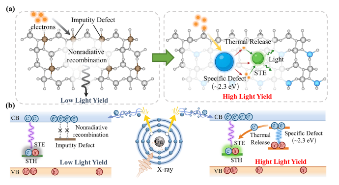
SCHEME 1 Defect-engineered energy relaxation pathways for enhanced light yield in β-Ga2O3. (a) Atomic-scale configuration and (b) the corresponding band structure.
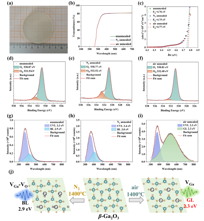
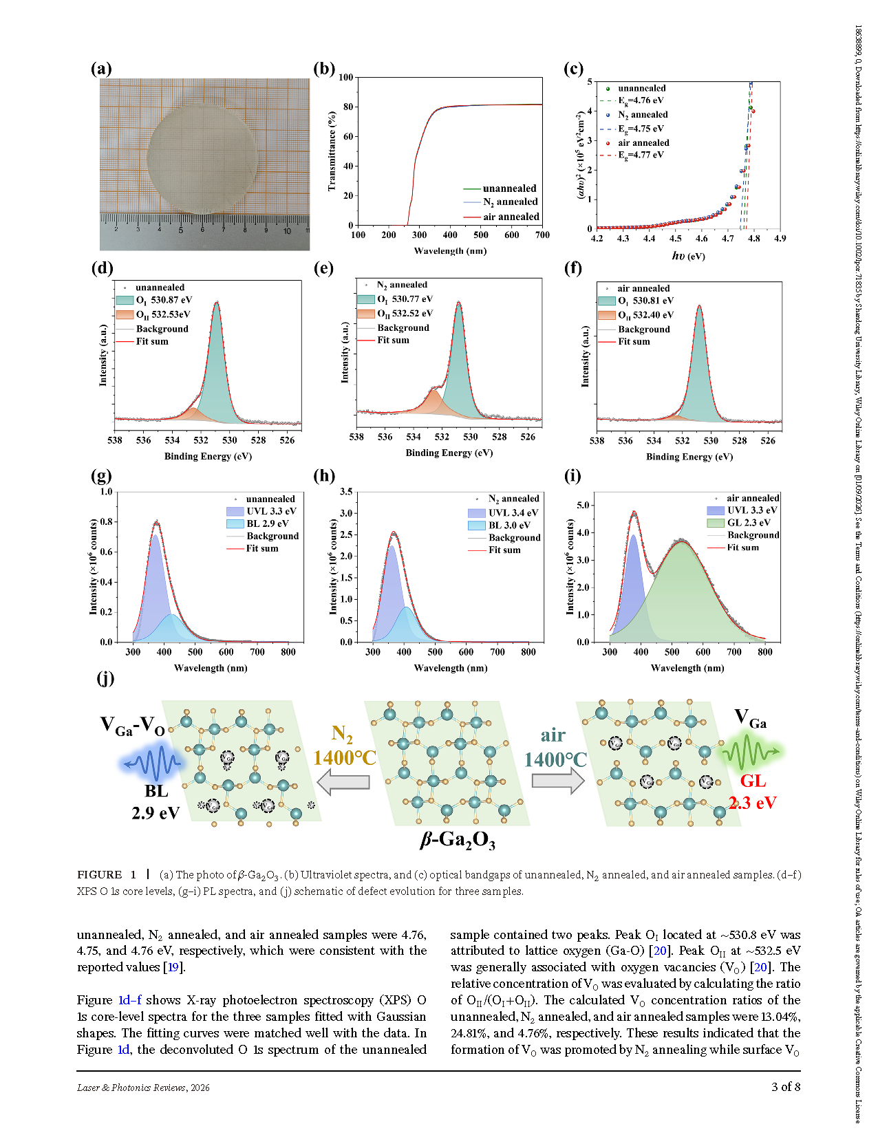
FIGURE 1 (a) The photo of β-Ga2O3. (b) Ultraviolet spectra, and (c) optical bandgaps of unannealed, N2 annealed, and air annealed samples. (d–f) XPS O 1s core levels, (g–i) PL spectra, and (j) schematic of defect evolution for three samples.
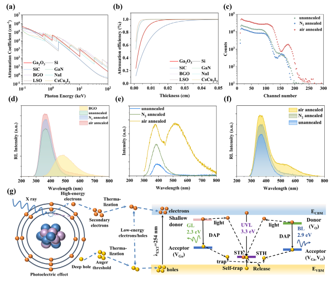
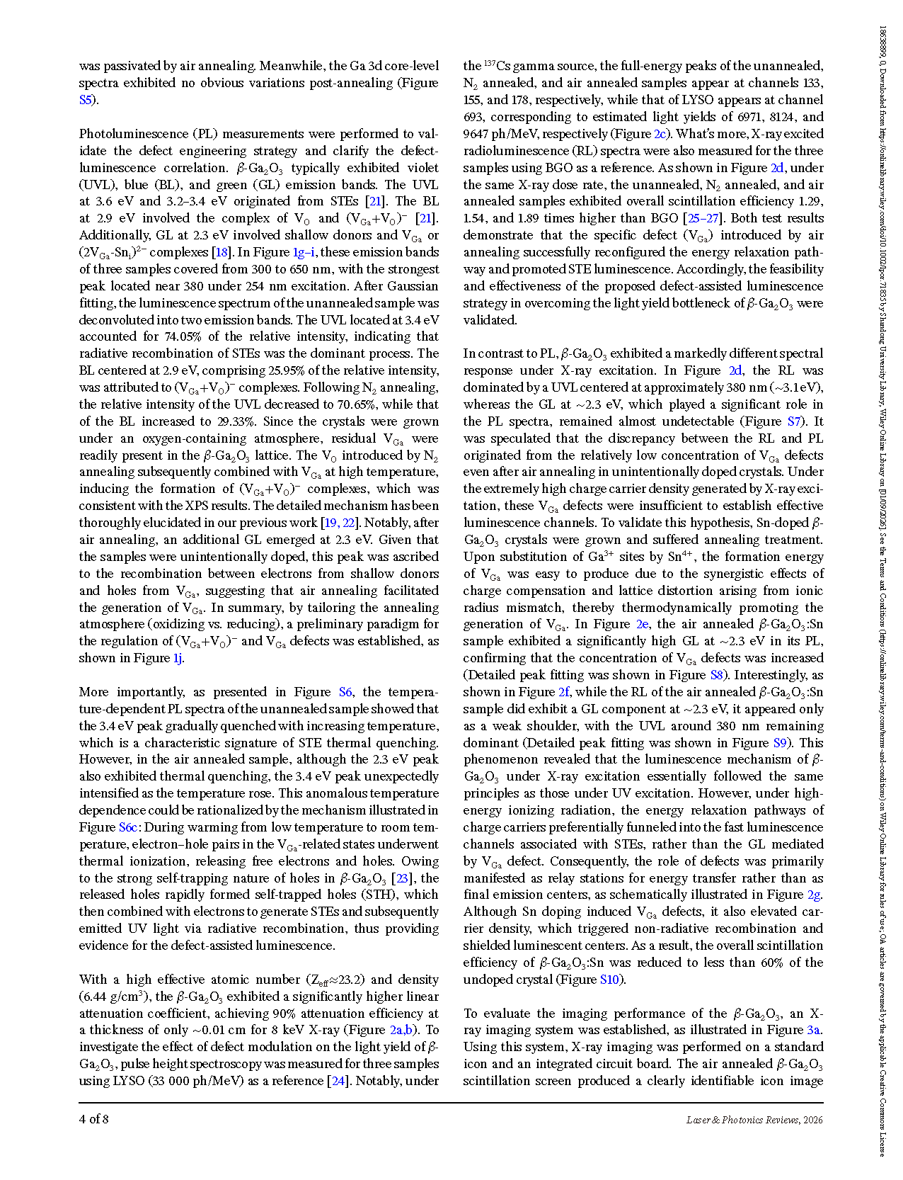
FIGURE 2 (a) Photon energy attenuation coefficients and (b) thickness-dependent attenuation efficiency of β-Ga2O3 vs. traditional scintillators (8 keV). (c) 137Cs Pulse height spectra of unannealed, N2 annealed, and air annealed samples. (d) RL spectra of unannealed and annealed samples. (e) PL and (f) RL spectra of β-Ga2O3:Sn before and after annealing. (g) Schematic of the RL mechanism under X-ray excitation.
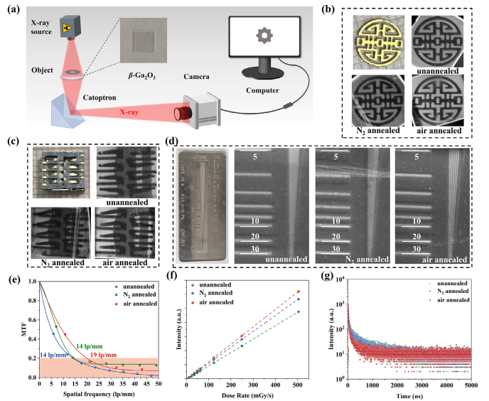
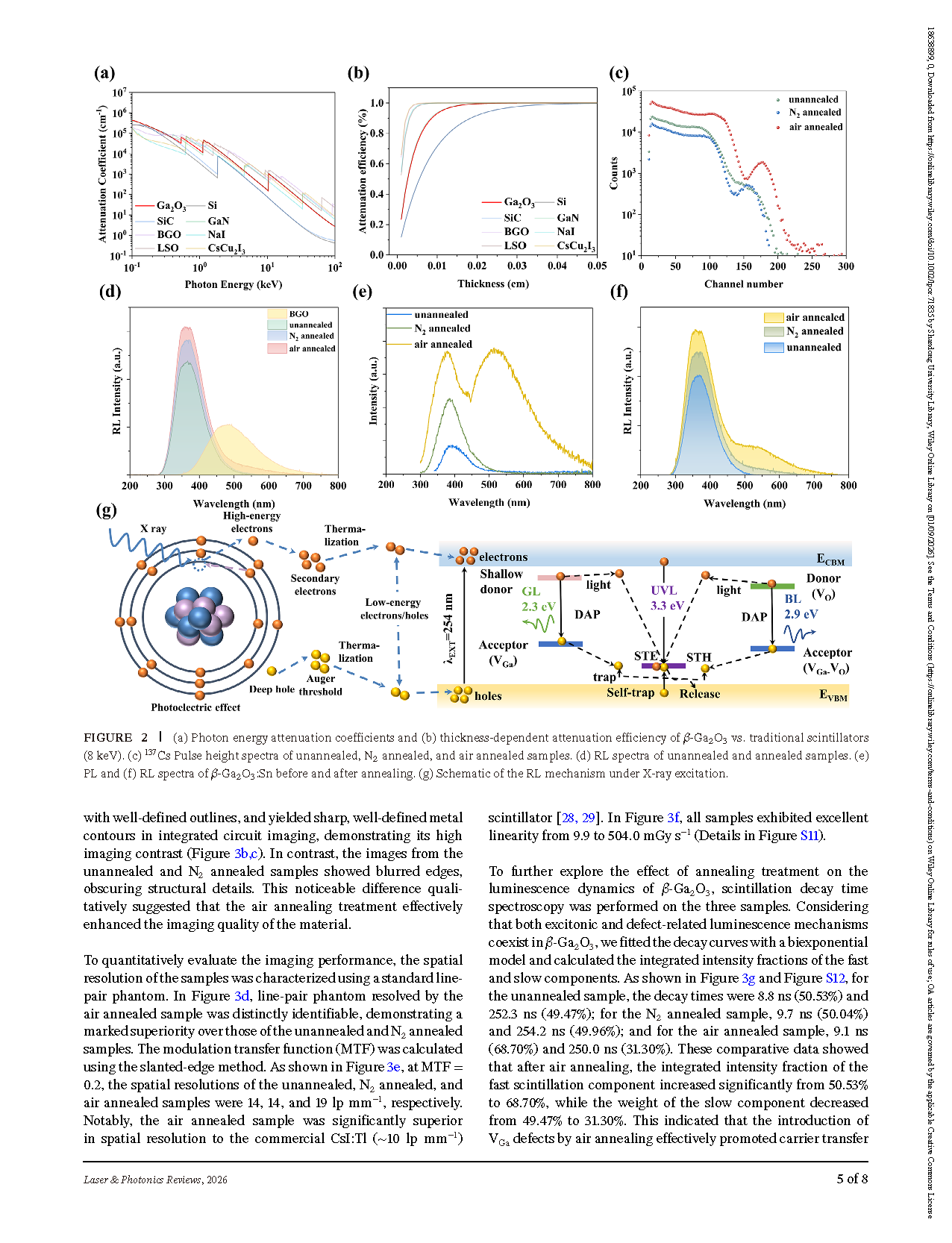
FIGURE 3 (a) X-ray imaging system schematic. X-ray images of(b) an icon,(c)IC board, and (d)line-pair phantom using unannealed and annealed samples. (e) MTF curves and (f) RL intensity vs. dose rate for all three samples. (g) Scintillation decay time spectroscopy of the three samples.
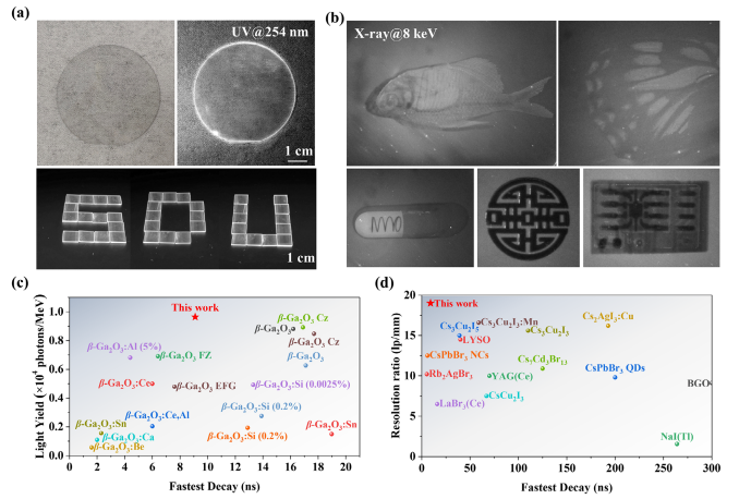
FIGURE 4 (a) Photo of a 2-inch β-Ga2O3 crystal under 254 nm light irradiation. (b) X-ray images of 2-inch β-Ga2O3 crystal. (c) Comparison of the light yield and Decay time of β-Ga2O3 crystals. (d) Comparison of the Resolution ratio and Decay time reported previously based on Scintillator.
DOI:
doi.org/10.1002/lpor.71835
Instruction
Official Account

Cooperation
Top
