


As power devices continue to evolve toward higher voltages and greater efficiency, the materials that power these advances are becoming an increasingly critical issue for the industry.
The adoption of 800 V high-voltage platforms in new energy vehicles is accelerating, ultra-high-voltage direct-current (UHVDC) transmission networks continue to expand, and energy storage converters face growing demands for lower power losses and smaller form factors. Together, these applications point to a common need: semiconductor materials capable of withstanding higher voltages, reducing losses, and delivering greater power density.
Following silicon carbide (SiC), gallium oxide (β-Ga₂O₃) is regarded as a promising candidate for next-generation high-voltage power applications. Its theoretical breakdown electric field is approximately two to three times that of SiC. Moreover, gallium oxide crystals can be grown directly from the melt, giving the material significant potential for low-cost, large-diameter wafer production.
However, for gallium oxide to make its way into end-use applications, the first major hurdle lies not in device design, but at the very beginning of the supply chain: the substrate.
Why Is (001) So Challenging, and Why Does “Twin-Free” Deserve Special Attention?
For β-Ga₂O₃ used in high-voltage epitaxy, crystal-plane selection directly affects defect formation, nucleation, and the consistency of subsequent devices. The (001) orientation is well suited to several mainstream epitaxial growth approaches, but it also presents significant growth challenges.
On the one hand, gallium oxide is relatively brittle, and certain crystallographic planes exhibit a tendency to cleave, making the crystal susceptible to cracking during crystal pulling and subsequent processing. On the other hand, producing specific orientations such as (001) and (010) via edge-defined film-fed growth (EFG) often requires cutting wafers from the side of a thick crystal. Inadequate control of the thermal field, die design, necking, and growth interface can lead to macroscopic defects, including twins, grain boundaries, bubbles, and inclusions.
For (001) in particular, once a twin forms, it can propagate along a cleavage plane throughout the entire crystal boule, making it virtually impossible to eliminate through downstream processing. This is precisely why twin-free growth is regarded as a critical requirement for (001) substrates.
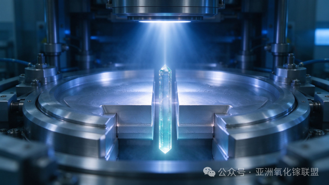
The larger the crystal, the more pronounced these challenges become. At the 2-inch scale, process experience may be sufficient to establish a workable growth process. At 4 inches, batch-to-batch consistency becomes a key concern. At 6 inches and beyond, manufacturers must simultaneously address thermal-field symmetry, stress relaxation, twin suppression, wafer warpage during processing, and subsurface damage.
As is often noted in the industry, growing gallium oxide crystals is not necessarily the hardest part; the real challenge is producing substrates suitable for epitaxy and wafer slicing that can be manufactured consistently and supplied repeatedly.
SINOGa Valley Semiconductor’s Approach: Proprietary EFG Technology Targeting Twin-Free (001) Crystals
SINOGa Valley Semiconductor has established a production line covering raw material preparation, crystal growth, substrate processing, and inspection and evaluation. Led by a PhD-level team, the company has adopted its own edge-defined film-fed growth (EFG) approach, focusing on the growth of twin-free single-crystal β-Ga₂O₃ with a (001) orientation.
The company has now established an integrated process chain spanning single-crystal growth through substrate processing:
2–4-inch twin-free (001) gallium oxide substrates:Stable batch production and delivery have been achieved, supporting research and development as well as small- to medium-volume device validation.
6-inch products:Trial production has been completed, and the company is capable of supplying small batches, laying the groundwork for larger wafer sizes and lower unit costs.
Key crystal performance metrics: The company reports that its key crystal parameters have reached an advanced level among comparable technologies documented in publicly available international reports.
Turning a single crystal boule grown in the laboratory into substrate wafers that can be delivered consistently on a production line requires thousands of growth runs, process adjustments, defect inspections, and parameter iterations. A true breakthrough is not the result of a single stroke of inspiration, but the ability to transform “crystal growth is possible” into “crystal growth is stable and reproducible.”
Of course, building a viable gallium oxide industry requires more than advances in substrate technology alone. Precise doping, epitaxial growth processes, device architectures, and reliability validation all require close collaboration between substrate manufacturers and device manufacturers.
Looking at broader industry trends, whether in 800 V high-voltage platforms, ultra-high-voltage power transmission, or large-scale energy storage, the availability of advanced substrates without dependence on overseas suppliers would give companies greater confidence in incorporating gallium oxide into their product roadmaps. This, in turn, could help China’s semiconductor industry move beyond following international developments toward greater technological independence and supply chain control.
Stabilizing the production of twin-free (001) gallium oxide substrates and advancing toward the forefront of the global semiconductor industry—this is the path and ambition of SINOGa Valley Semiconductor. The company aims to make reliable, China-made substrates a viable option for the era of high-voltage power electronics. It also looks forward to working with industry partners to bring gallium oxide from material research into real-world industrial applications.
Instruction
Official Account

Cooperation
Top
