


The team led by Academician Yue Hao and Prof. Genquan Han at Xidian University has published a research article entitled “Low turn-on voltage and improved interface properties of β-Ga₂O₃ Schottky barrier diodes with NH₃ plasma treatment” in Applied Physics Letters. Associate Professor Yibo Wang and Prof. Genquan Han are the corresponding authors.
Background
β-Ga₂O₃ features an ultrawide bandgap, a high critical electric field, and the availability of large-size bulk single-crystal substrates grown by melt-based techniques, making it an important candidate for high-voltage and high-power electronic devices. Among various device architectures, Schottky barrier diodes (SBDs), with their simple structure and fast switching speed, represent an important research direction for β-Ga₂O₃ power rectifiers.
In recent years, research on the breakdown performance of β-Ga₂O₃ SBDs has mainly focused on electric-field management techniques such as field plates and edge termination. However, the metal/β-Ga₂O₃ interface itself also plays an important role in determining device performance. Oxygen vacancies, suboxides, adsorbed species, and impurity-related defects near the interface may modify the Schottky barrier and local electric field and participate in reverse carrier transport, thereby affecting the turn-on voltage, leakage current, and breakdown characteristics.
Existing approaches such as oxygen annealing, surface etching, and post-annealing can improve the β-Ga₂O₃ Schottky interface to some extent, but some treatments may increase the specific on-resistance or be highly sensitive to the process window and subsequent fabrication steps. Therefore, simultaneously improving interface quality while maintaining a low turn-on voltage and low conduction loss remains an important challenge in β-Ga₂O₃ SBD interface engineering.
To address this issue, this work employs remote NH₃ plasma treatment of the β-Ga₂O₃ surface to regulate the chemical state of the Schottky interface and reduce the turn-on voltage. Conductance measurements, XPS, and forward/reverse electrical characterization are further combined to systematically investigate the effects of NH₃ plasma treatment on interface defects and carrier transport mechanisms.
Abstract
1.NH₃ plasma treatment reduces the turn-on voltage and improves forward conduction
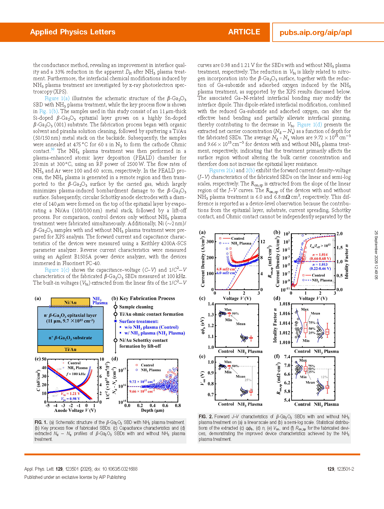
The research team employed PEALD-based remote NH₃ plasma treatment on the β-Ga₂O₃ surface and fabricated Ni/Au Schottky barrier diodes. The carrier concentration in the epitaxial layer remains nearly unchanged before and after treatment, indicating that the plasma treatment mainly affects the near-surface region.
Forward measurements show that the Schottky barrier height decreases from 1.32 to 1.09 eV, the turn-on voltage decreases from 0.96 to 0.73 V, and the specific on-resistance decreases from 6.8 to 6.0 mΩ·cm². At 3 V, the current density increases from 267 to 341 A/cm².
2.Reduced interface-defect response and modified interfacial chemical states
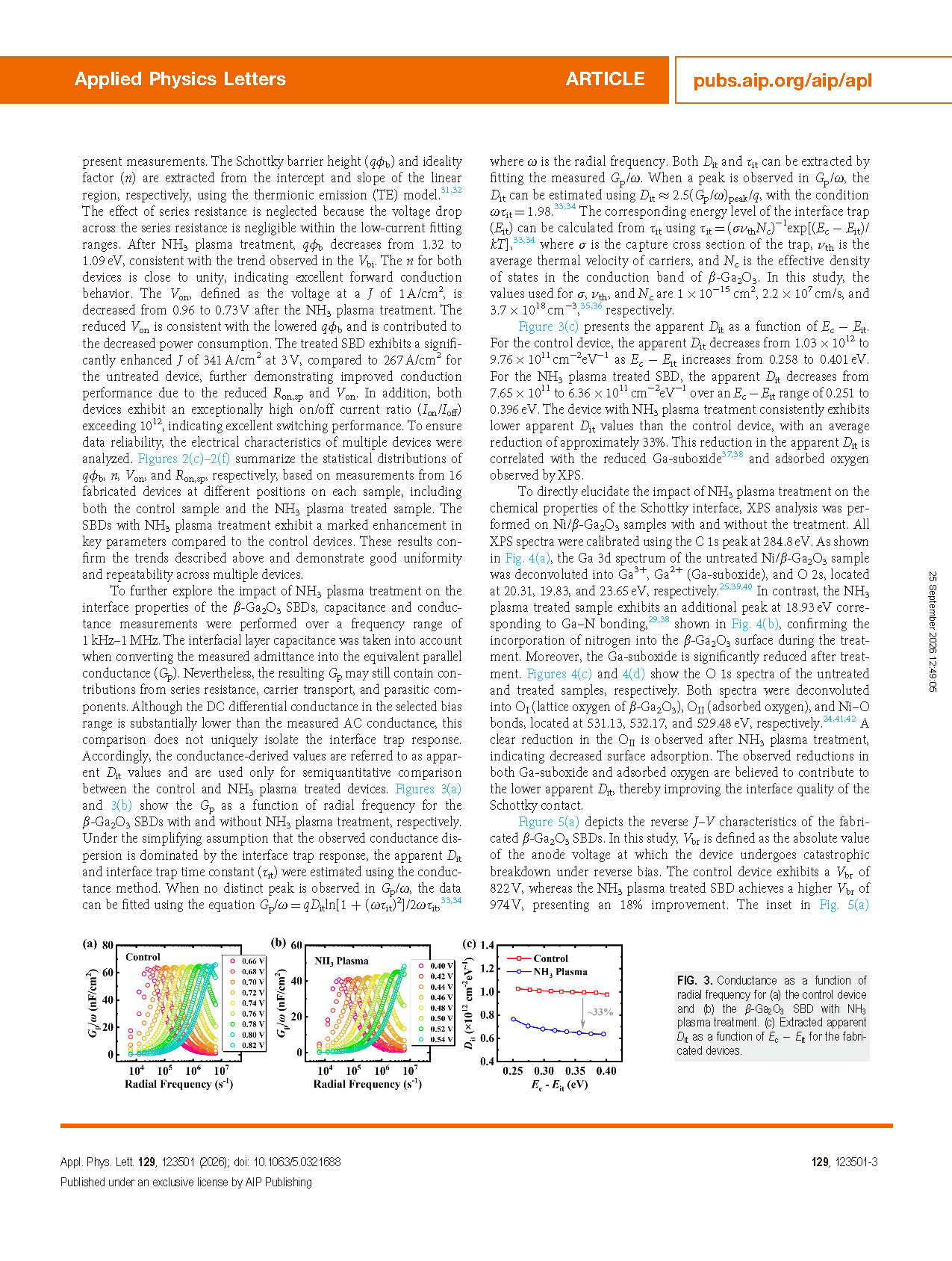
Frequency-dependent conductance measurements show that the apparent interface state density Dit decreases by approximately 33% after NH₃ plasma treatment.
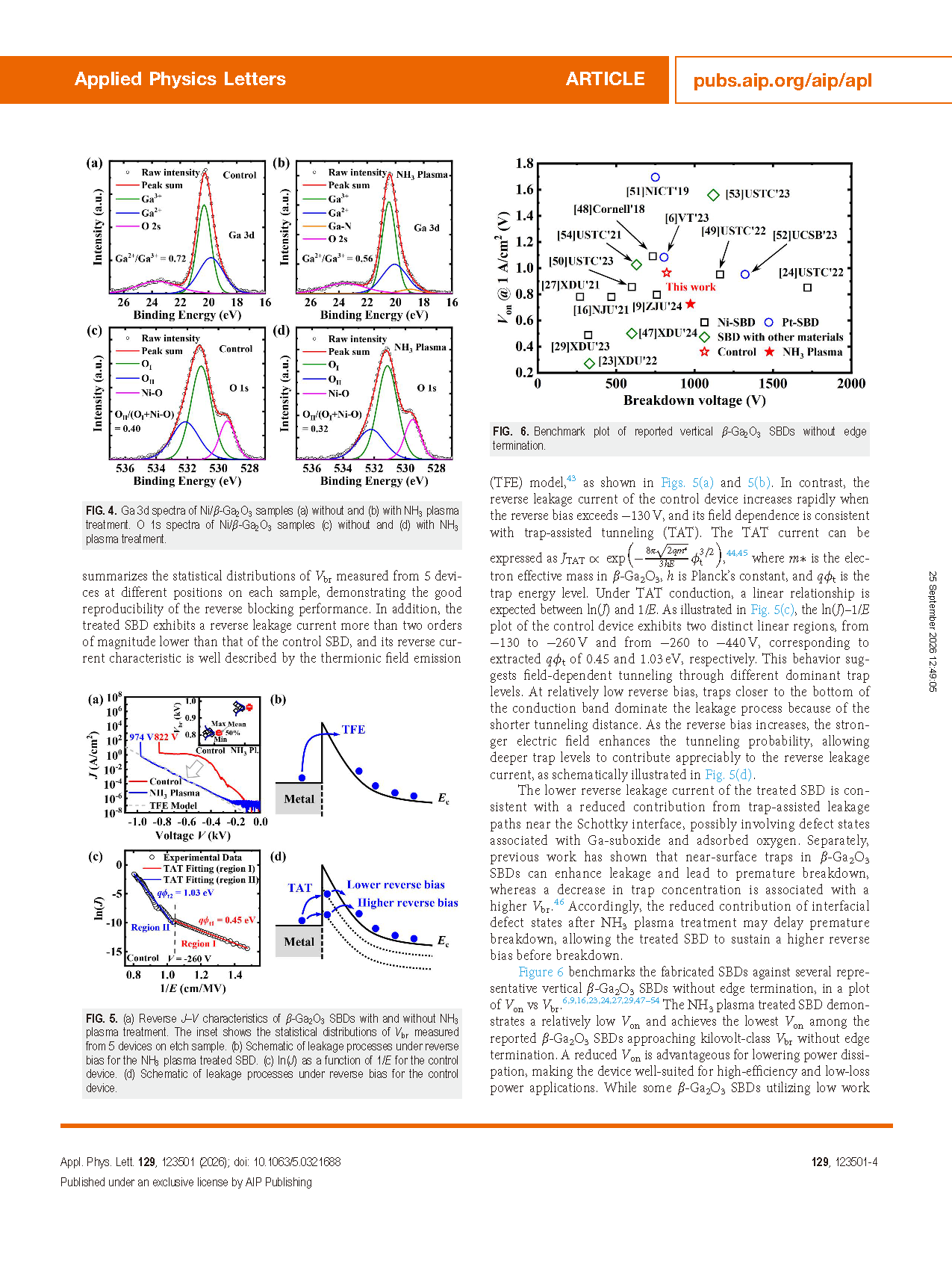
XPS results reveal the formation of Ga–N bonds on the treated β-Ga₂O₃ surface, accompanied by reductions in Ga suboxide and adsorbed oxygen, demonstrating that NH₃ plasma treatment effectively modifies the chemical states and defect characteristics of the Schottky interface.
3.Reduced reverse leakage and an 18% increase in breakdown voltage
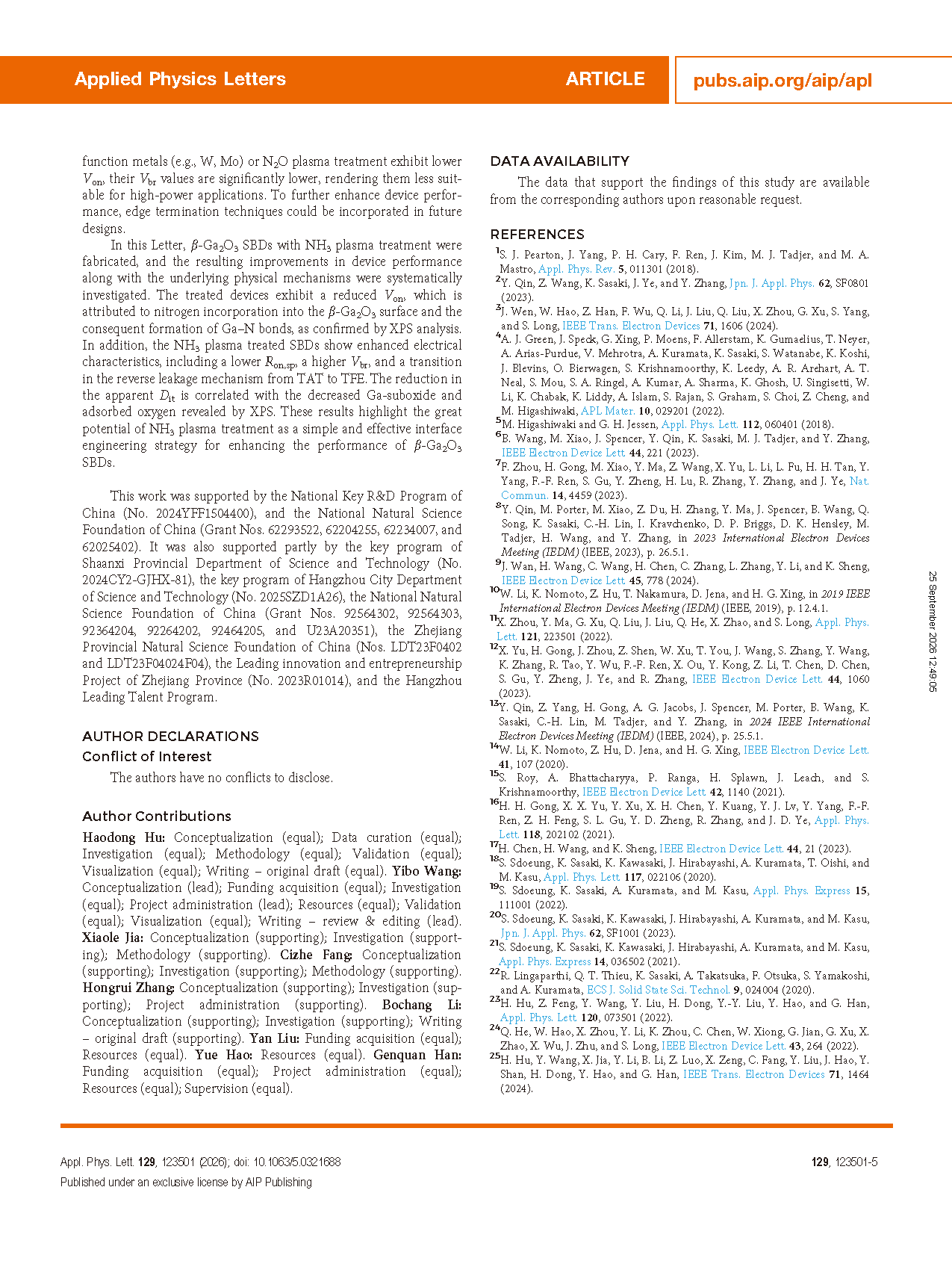
After NH₃ plasma treatment, the reverse leakage current is reduced by more than two orders of magnitude, while the dominant reverse transport mechanism changes from trap-assisted tunneling (TAT) in the control device to thermionic-field emission (TFE).
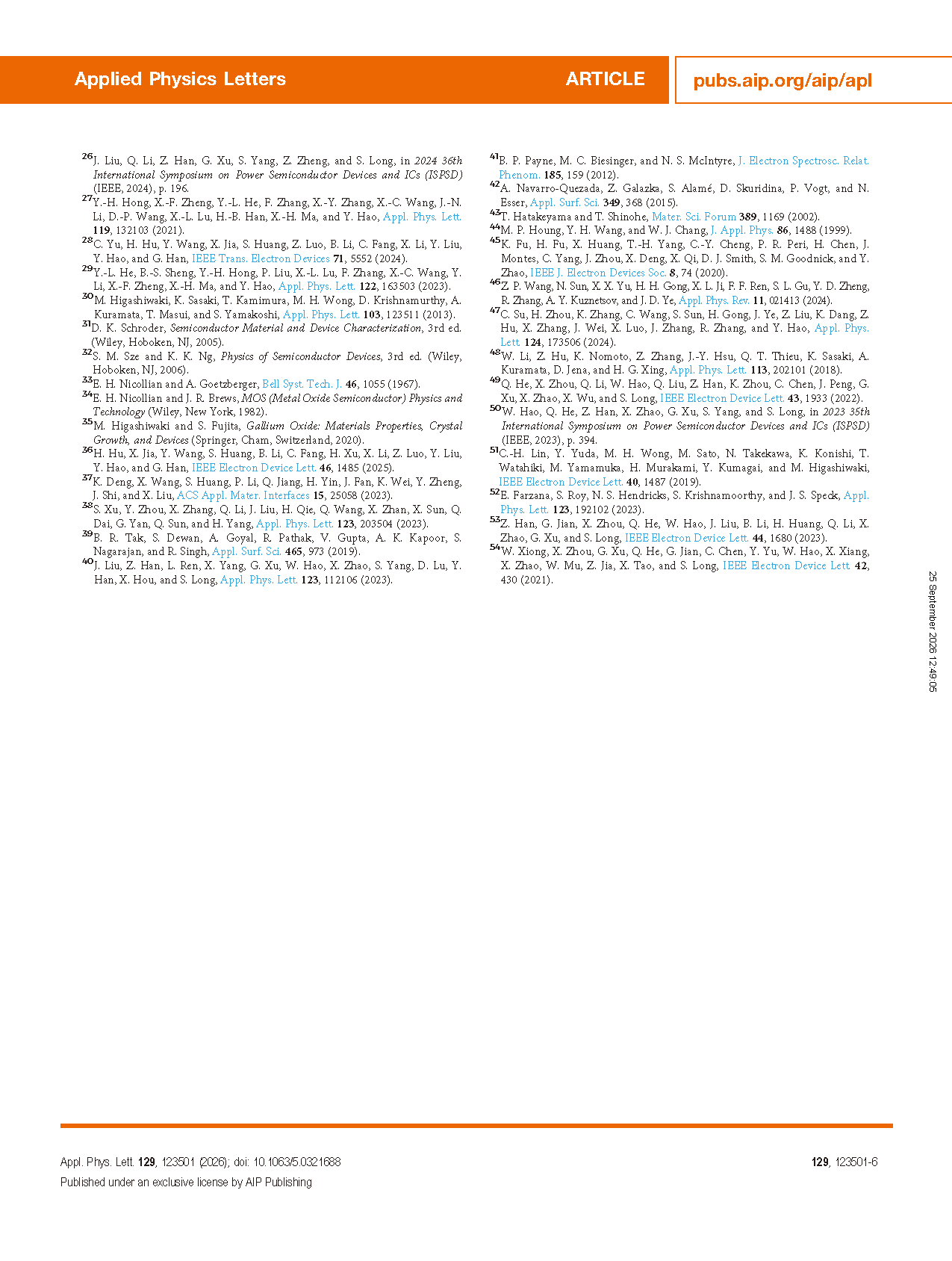
Meanwhile, the breakdown voltage increases from 822 to 974 V, corresponding to an improvement of approximately 18%. Among vertical β-Ga₂O₃ SBDs without edge termination, the device combines a low turn-on voltage of 0.73 V with a breakdown capability approaching the kilovolt level.
Highlights
① First, an NH₃ plasma-based Schottky interface-engineering approach is proposed. Remote plasma treatment modifies the chemical state of the β-Ga₂O₃ surface while minimizing direct physical bombardment, enabling a low turn-on voltage of 0.73 V together with a low specific on-resistance.
② Second, a correlation among interfacial chemical states, defect response, and carrier transport is established. XPS reveals the formation of Ga–N bonds and reductions in Ga suboxide and adsorbed oxygen, while conductance measurements show an approximately 33% reduction in apparent Dit. Meanwhile, the reverse transport mechanism changes from TAT to TFE, providing complementary evidence for the modulation of the Schottky interface by NH₃ plasma treatment.
③ Finally, forward conduction and reverse blocking characteristics are simultaneously improved. While the turn-on voltage decreases from 0.96 to 0.73 V, the reverse leakage current is significantly suppressed and the breakdown voltage increases from 822 to 974 V, providing a new interface-engineering strategy for β-Ga₂O₃ SBDs that combines low conduction loss with high blocking capability.
Conclusion
This work demonstrates chemical-state modulation of the β-Ga₂O₃ Schottky interface through remote NH₃ plasma treatment.
The results show that NH₃ plasma treatment induces Ga–N-related bonding on the β-Ga₂O₃ surface while reducing Ga suboxide and adsorbed oxygen, resulting in an average reduction of approximately 33% in the apparent interface state density. Correspondingly, the device turn-on voltage decreases from 0.96 to 0.73 V, the reverse carrier transport mechanism changes from TAT to TFE, and the breakdown voltage increases from 822 to 974 V.
These results indicate that plasma-induced regulation of the near-surface chemical and defect states of β-Ga₂O₃ provides an effective interface-engineering approach for improving Schottky interface quality, reducing conduction loss, and enhancing reverse blocking performance.
Project Support
This work was supported by the National Key R&D Program of China (2024YFF1504400); the National Natural Science Foundation of China (62293522, 62204255, 62234007, 62025402, 92564302, 92564303, 92364204, 92264202, 92464205, and U23A20351); the Key Program of the Shaanxi Provincial Department of Science and Technology (2024CY2-GJHX-81); the Key Program of the Hangzhou Municipal Science and Technology Bureau (2025SZD1A26); the Natural Science Foundation of Zhejiang Province (LDT23F0402 and LDT23F04024F04); the Leading Innovation and Entrepreneurship Project of Zhejiang Province (2023R01014); and the Hangzhou Leading Talent Program.
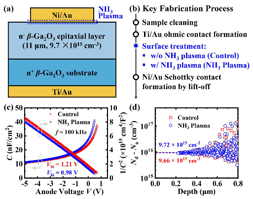
Fig. 1. Device structure, key fabrication process, C–V characteristics, and carrier concentration profiles of β-Ga₂O₃ SBDs with NH₃ plasma treatment.
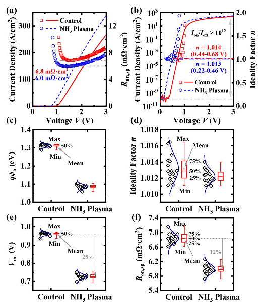
Fig. 2. Forward J–V characteristics of β-Ga₂O₃ SBDs with and without NH₃ plasma treatment, together with the statistical distributions of barrier height, ideality factor, turn-on voltage, and specific on-resistance.
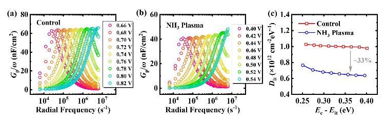
Fig. 3. Frequency-dependent conductance characteristics and extracted apparent interface state density of β-Ga₂O₃ SBDs with and without NH₃ plasma treatment.
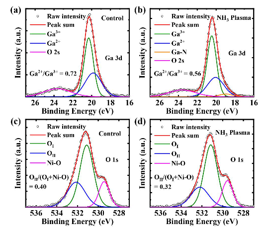
Fig. 4. Ga 3d and O 1s XPS spectra of Ni/β-Ga₂O₃ samples with and without NH₃ plasma treatment.
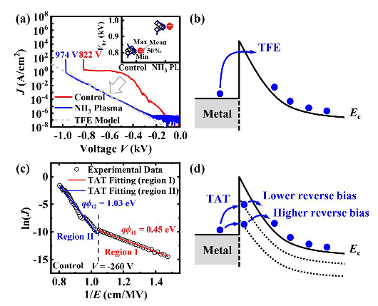
Fig. 5. Reverse J–V characteristics of β-Ga₂O₃ SBDs and schematic illustrations of the different reverse carrier transport mechanisms.
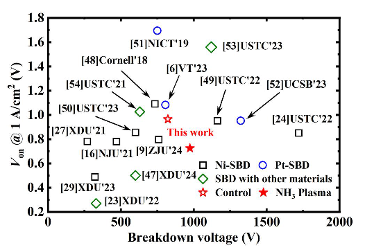
Fig. 6. Benchmark of turn-on voltage and breakdown voltage for reported vertical β-Ga₂O₃ SBDs without edge termination.
DOI:
doi.org/10.1063/5.0321688
Instruction
Official Account

Cooperation
Top
