


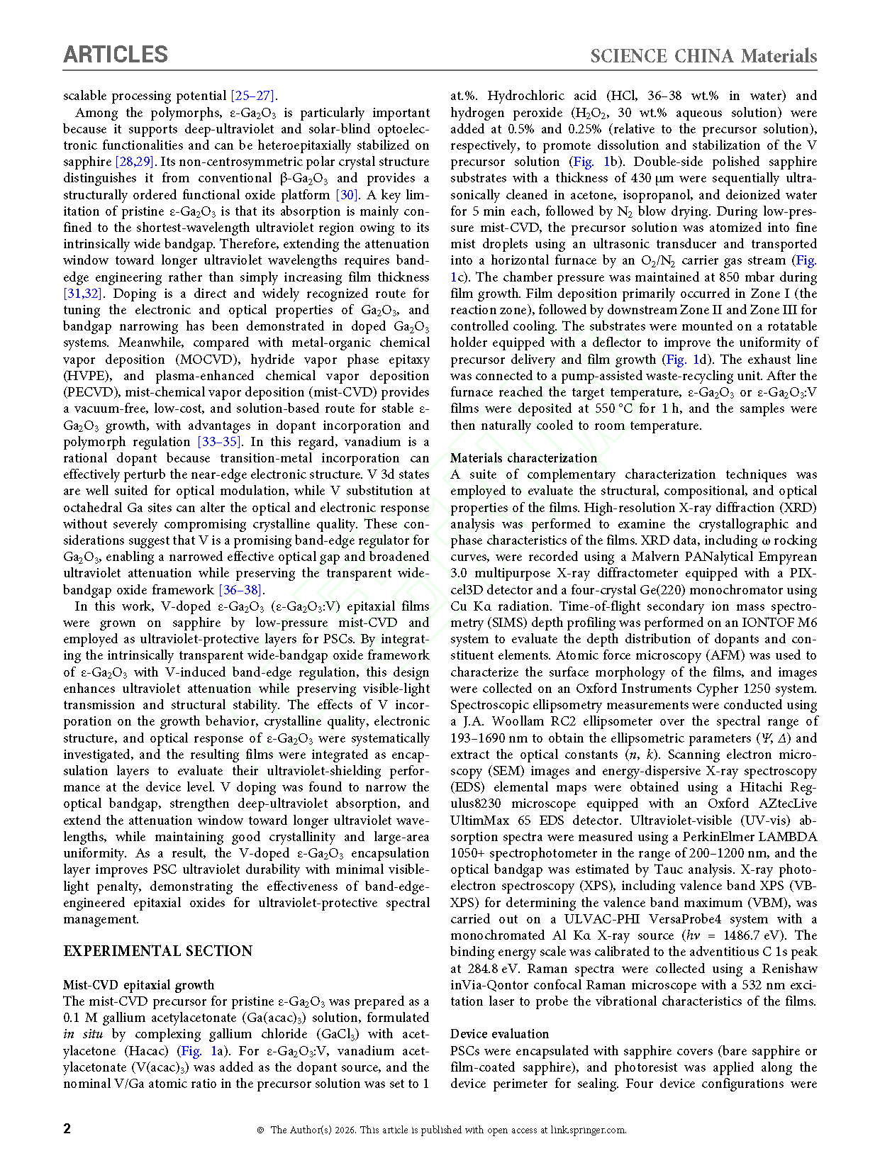
Researchers from The Hong Kong University of Science and Technology (Guangzhou) and Nanjing University of Posts and Telecommunications have published a dissertation titled "Bandgap‑engineered ε‑Ga₂O₃ with enhanced ultraviolet absorption for high‑efficiency and photostable perovskite solar cells" in SCIENCE CHINA Materials.
Background
Ultraviolet‑induced degradation is a major challenge for perovskite solar cells (PSCs). High‑energy ultraviolet photons accelerate defect generation, ion migration and interfacial degradation, seriously impairing long‑term device stability. An ideal ultraviolet‑protective material should combine efficient ultraviolet attenuation, high visible‑light transmittance and outstanding stability under harsh conditions. Current strategies to improve the ultraviolet durability of PSCs mainly include interface engineering, internal ultraviolet‑absorbing or passivating interlayers, and external spectral‑management encapsulation and filtering. Interface‑centered approaches strongly depend on device architecture and processing procedures. Built‑in ultraviolet‑absorbing interlayers often bring optical loss and interfacial complexity. By contrast, external spectral‑management schemes can realize non‑invasive photonic protection without modifying internal functional layers and exhibit prominent advantages. Gallium oxide (Ga₂O₃), an ultrawide‑bandgap oxide semiconductor, features deep‑ultraviolet response, high visible‑light transmittance and excellent thermal and chemical stability. Among its polymorphs, ε‑Ga₂O₃ can be heteroepitaxially grown on sapphire. Nevertheless, pristine ε‑Ga₂O₃ mainly absorbs short‑wavelength ultraviolet light, so band‑edge engineering is required to broaden its ultraviolet attenuation window. Mist‑chemical vapor deposition (mist‑CVD) is a vacuum‑free, low‑cost solution‑based thin‑film fabrication technique. As a transition‑metal dopant, vanadium (V) is expected to modulate the near‑band‑edge electronic structure of ε‑Ga₂O₃, achieving bandgap narrowing and extended ultraviolet absorption while preserving the host crystal framework.
Abstract
Ultraviolet‑induced degradation remains a critical obstacle to the long‑term stability of perovskite solar cells (PSCs). Current protection strategies mainly rely on interfacial modification or internal ultraviolet‑absorbing layers, which may introduce processing complexity and optical loss. This study reports vanadium‑doped ε‑gallium oxide (ε‑ Ga₂O₃:V) epitaxial films grown on sapphire by low‑pressure mist chemical vapor deposition (mist‑CVD) for use as ultraviolet‑protective encapsulation layers for PSCs. V incorporation regulates the band‑edge electronic structure of ε‑ Ga₂O₃ while preserving its crystal structure, crystallinity, and large‑area uniformity. The optical bandgap narrows from 4.56 to 4.40 eV, deep‑ultraviolet absorption is enhanced, and the attenuation window extends from the intrinsic ultraviolet C region into the ultraviolet B and part of the ultraviolet A region while maintaining low visible‑light loss. First‑principles calculations indicate that V preferentially substitutes at the Ga II site and reconstructs the near‑band‑edge electronic structure through hybridized V 3d and O 2p states, accounting for the red‑shifted absorption edge. With ε‑ Ga₂O₃:V‑coated sapphire as the encapsulation layer, PSCs sustain a power conversion efficiency (PCE) of 20.14 % after 1000 h of continuous 254 nm ultraviolet irradiation, extending the ultraviolet operational lifetime by more than fourfold relative to bare‑sapphire‑encapsulated PSCs. This work establishes a band‑edge‑engineering route for transparent oxide encapsulation and ultraviolet‑protective spectral management in perovskite photovoltaics.
Highlights
The team successfully grew vanadium-doped ε‑Ga₂O₃ (ε‑Ga₂O₃:V) epitaxial films on sapphire via low-pressure mist-CVD and employed them as non-invasive external encapsulation layers for PSCs.
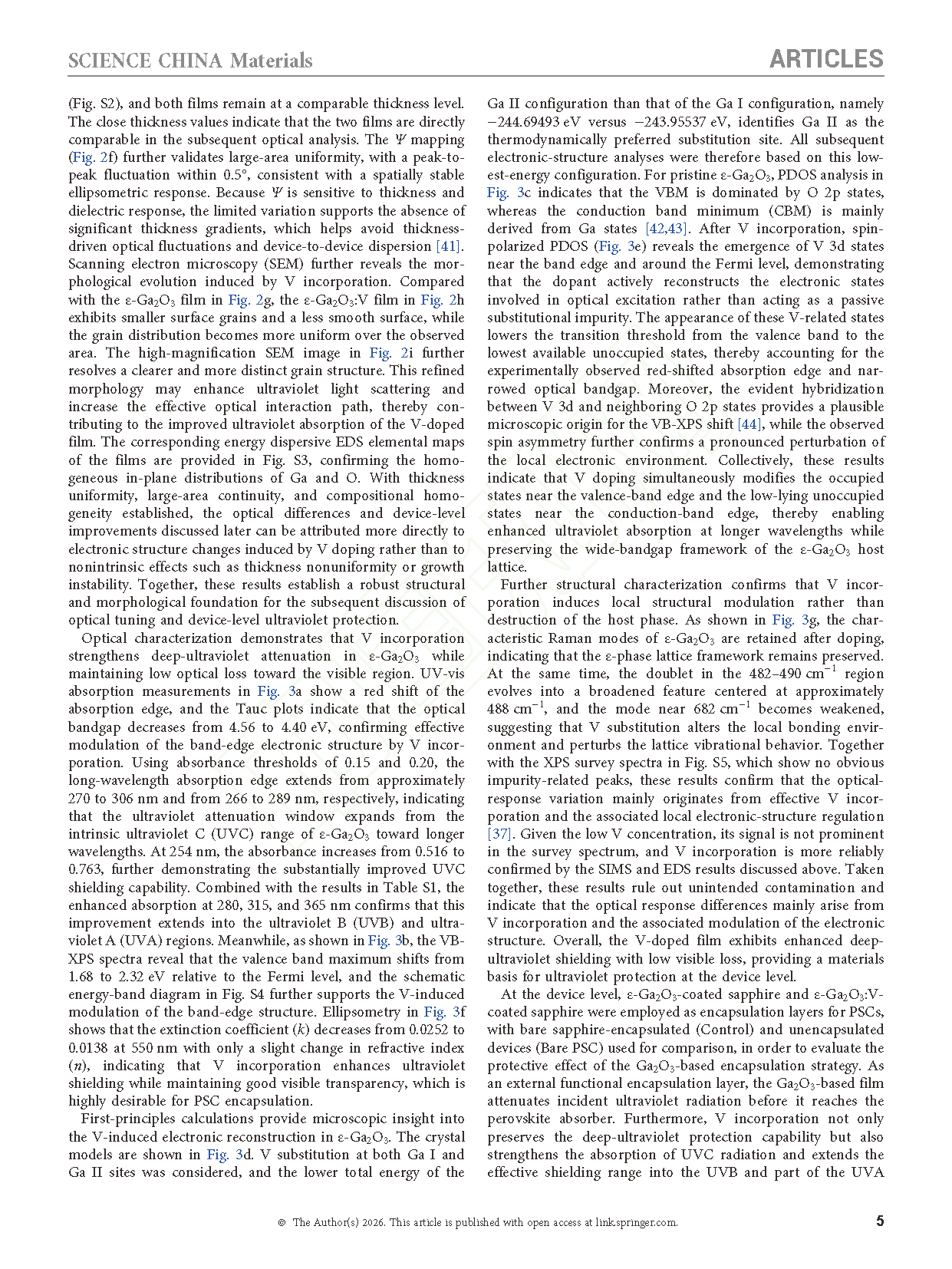
V doping effectively narrowed the optical bandgap of ε‑Ga₂O₃ (from 4.56 to 4.40 eV), significantly enhanced deep-ultraviolet absorption, and extended the attenuation window from the UVC region into the UVB and part of the UVA region while maintaining low visible-light loss.
First-principles calculations revealed that V preferentially substitutes at the Ga II site and reconstructs the near-band-edge electronic structure via hybridization of V 3d and O 2p states, providing a microscopic explanation for the red-shifted absorption edge and enhanced UV absorption.
PSCs encapsulated with ε‑Ga₂O₃:V achieved a high initial PCE of 25.46% and maintained a PCE of 20.14% after 1000 h of continuous 254 nm UV irradiation.
Compared to bare-sapphire-encapsulated control devices, theε‑Ga₂O₃:V encapsulation extended the UV operational lifetime of PSCs by more than fourfold, demonstrating superior UV stability.
Conclusion
This study systematically investigates the effects of V doping on the growth, electronic structure, optical response, and ultraviolet‑shielding function of ε‑Ga₂O₃ epitaxial films for perovskite solar cell encapsulation. By introducing V into ε‑Ga₂O₃ through low‑pressure mist‑CVD growth on sapphire substrates, we successfully achieved enhanced deep‑ultraviolet attenuation while preserving the ε‑phase framework, high crystallinity, and good large‑area uniformity. The results show that V incorporation narrows the optical bandgap from 4.56 to 4.40 eV, strengthens UVC absorption, and extends the ultraviolet attenuation window toward the UVB and part of the UVA region, while maintaining low visible‑region optical loss. First‑principles calculations further reveal that V substitution preferentially occurs at the Ga II site and reconstructs the near‑band‑edge electronic structure through V 3d‑related states and their hybridization with O 2p states, thereby providing a microscopic origin for the red‑shifted absorption edge and valence‑band modification. At the device level, the ε‑Ga₂O₃:V‑coated sapphire encapsulation layer delivers the highest initial PCE of 25.46 % and maintains a PCE of 20.14 % after 1000 h of continuous 254 nm ultraviolet irradiation, remaining above the defined 20 % failure threshold and extending the ultraviolet operational lifetime by more than fourfold relative to the Control device. Overall, V‑doped ε‑Ga₂O₃ functions as an effective spectral‑management encapsulation material that suppresses ultraviolet‑induced degradation with minimal visible‑light penalty. This work provides an effective strategy for ultraviolet‑protective encapsulation of PSCs and highlights its potential for stable photovoltaic operation in harsh irradiation conditions, particularly for space‑related applications.
Project Support
This work was supported by the C. K. Tan start-up fund from The Hong Kong University of Science and Technology (Guangzhou), the fund from Nanjing University of Posts and Telecommunications, the Guangzhou Municipal Science and Technology Project (2023A03J0003, 2023A03J0013, 2023A04J0310, 2023A03J0152), the Department of Education of Guangdong Province (2024ZDZX1005), the State Administration of Foreign Experts Affairs (Y20240005), and the National Natural Science Foundation of China (CZ118SC24007, CZ118SC25005, RK118QN24006).
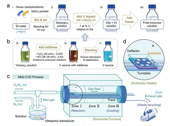
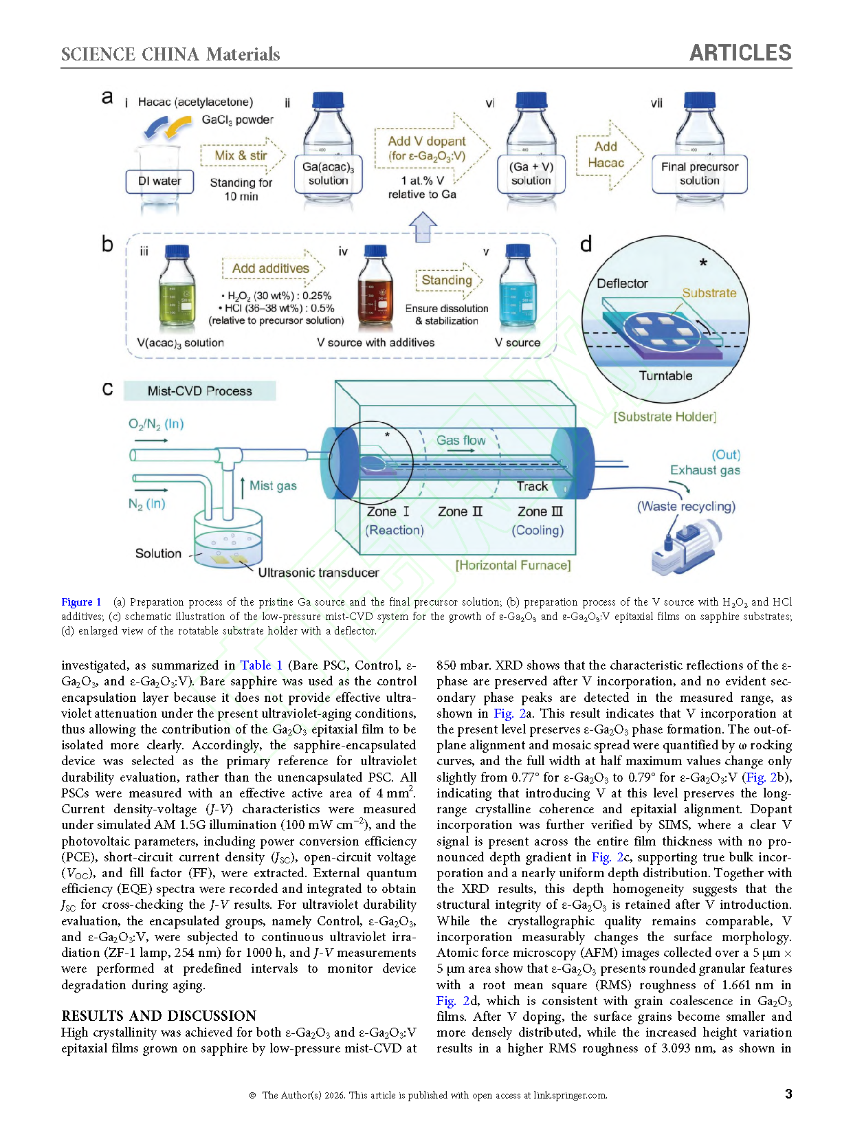
Fig. 1 (a) Preparation process of the pristine Ga source and the final precursor solution; (b) preparation process of the V source with H₂O₂ and HCl additives; (c) schematic illustration of the low-pressure mist-CVD system for the growth of ε‑Ga₂O₃ and ε‑Ga₂O₃:V epitaxial films on sapphire substrates; (d) enlarged view of the rotatable substrate holder with a deflector.
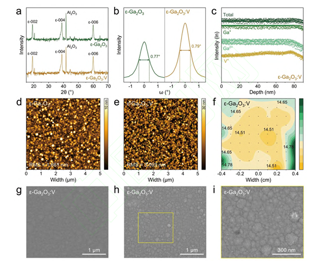
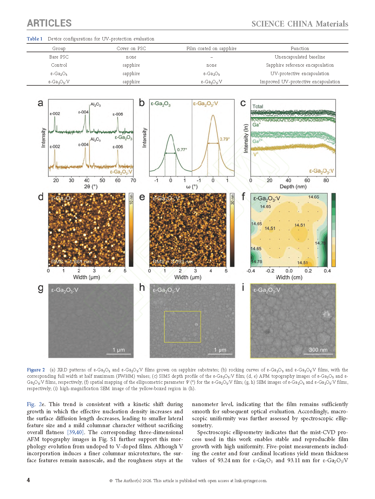
Fig. 2 (a) XRD patterns of ε‑Ga₂O₃ and ε‑Ga₂O₃:V films grown on sapphire substrates; (b) rocking curves of ε‑Ga₂O₃ and ε‑Ga₂O₃:V films, with the corresponding full width at half maximum (FWHM) values; (c) SIMS depth profile of the ε‑Ga₂O₃:V film; (d,e) AFM topography images of ε‑Ga₂O₃ and ε‑Ga₂O₃:V films, respectively; (f) spatial mapping of the ellipsometric parameter Ψ ε‑Ga₂O₃:V film; (g.h) SEM images of ε‑Ga₂O₃ and ε‑Ga₂O₃:V films, respectively; (i) high‑magnification SEM image of the yellow‑boxed region in (h).
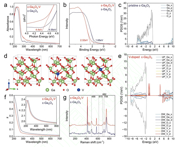
Fig. 3 (a) UV‑vis absorbance spectra of ε‑Ga₂O₃ and ε‑Ga₂O₃:V films, with the corresponding Tauc plots shown in the inset; (b) VB‑XPS spectra of ε‑Ga₂O₃ and ε‑Ga₂O₃:V films, with the extracted VBM positions; (c) orbital‑projected density of states of pristine ε‑Ga₂O₃; (d) crystal structure models of pristine ε‑Ga₂O₃ and V‑doped ε‑Ga₂O₃ with V substitution at Ga I and Ga II; (e) spin‑polarized orbital‑PDOS of V‑doped ε‑Ga₂O₃ based on the energetically favorable V substitution configuration; (f) extinction coefficient spectra of ε‑Ga₂O₃ and ε‑Ga₂O₃:V films, with the refractive index spectra shown in the inset; (g) Raman spectra of ε‑Ga₂O₃ and ε‑Ga₂O₃:V films.
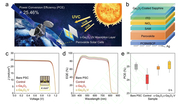
Fig. 4 (a) Schematic of the ε‑Ga₂O₃‑based ultraviolet shielding strategy for PSCs; (b) schematic device architecture of the PSC with the Ga₂O₃‑coated sapphire encapsulation layer; (c) J‑V curves of the Bare PSC, Control, ε‑Ga₂O₃ and ε‑Ga₂O₃:V devices at 0 h, with the inset showing the backside view of a representative device with Ag electrodes and an effective active area of 4 mm² highlighted in yellow; (d) EQE spectra and (e) box plots of PCE of the four corresponding devices at 0 h.
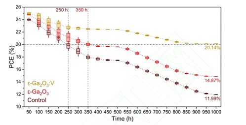
Fig. 5 PCE as a function of aging time for the Control, ε‑Ga₂O₃ and ε‑Ga₂O₃:V devices under continuous 254 nm ultraviolet irradiation for 1000 h, with the dashed line indicating the failure threshold defined at a PCE of 20 %. The ε‑Ga₂O₃:V devices remain above this threshold after 1000 h of aging, extending the ultraviolet operational lifetime by more than fourfold relative to the Control devices.
DOI:
10.1007/s40843‑026‑4421‑7
Instruction
Official Account

Cooperation
Top
