


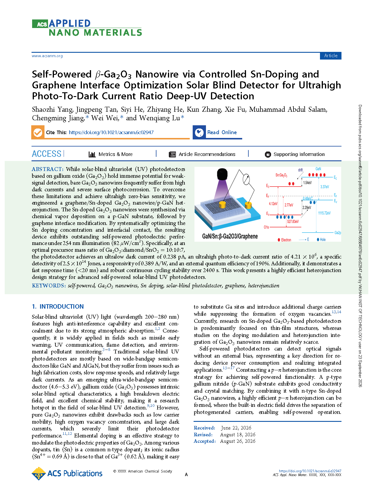
Researchers from the Chongqing Institute of Green and Intelligent Technology, Chinese Academy of Sciences, Chongqing University of Posts and Telecommunications, the University of Chinese Academy of Sciences, and Chongqing University have published a dissertation titled "Self-Powered β-Ga₂O₃ Nanowire via Controlled Sn-Doping and Graphene Interface Optimization Solar Blind Detector for Ultrahigh Photo-To-Dark Current Ratio Deep-UV Detection" in ACS Applied Nano Materials.
Background
Solar-blind ultraviolet (UV) light (wavelength 200−280 nm) features high anti-interference capability and excellent concealment due to its strong atmospheric absorption. Consequently, it is widely applied in fields such as missile early warning, UV communication, flame detection, and environmental pollutant monitoring. Traditional solar-blind UV photodetectors are mostly based on wide-bandgap semiconductors like GaN and AlGaN, but they suffer from issues such as high fabrication costs, slow response speeds, and relatively large dark currents. As an emerging ultra-wide-bandgap semiconductor (4.6−5.3 eV), gallium oxide (Ga₂O₃) possesses intrinsic solar-blind optical characteristics, a high breakdown electric field, and excellent chemical stability, making it a research hotspot in the field of solar-blind UV detection. However, pure Ga₂O₃ nanowires exhibit drawbacks such as low carrier mobility, high oxygen vacancy concentration, and large dark currents, which severely limit their photodetector performance. Elemental doping is an effective strategy to modulate the photoelectric properties of Ga₂O₃. Among various dopants, tin (Sn) is a common n-type dopant. Self-powered photodetectors can detect optical signals without an external bias, representing a key direction for reducing device power consumption and realizing integrated applications. Constructing a p-n heterojunction is the core strategy for achieving self-powered functionality. Furthermore, graphene possesses ultra-high carrier mobility, excellent optical transparency, and superior electrical conductivity. Nevertheless, the direct surface modification of highly crystalline Sn-doped β-Ga₂O₃ nanowire networks by graphene remains largely unexplored.
Abstract
While solar-blind ultraviolet (UV) photodetectors based on gallium oxide (Ga₂O₃) hold immense potential for weak-signal detection, bare Ga₂O₃ nanowires frequently suffer from high dark currents and severe surface photocorrosion. To overcome these limitations and achieve ultrahigh zero-bias sensitivity, we engineered a graphene/Sn-doped Ga₂O₃ nanowire/p-GaN heterojunction. The Sn-doped Ga₂O₃ nanowires were synthesized via chemical vapor deposition on a p-GaN substrate, followed by graphene interface modification. By systematically optimizing the Sn doping concentration and interfacial contact, the resulting device exhibits outstanding self-powered photoelectric performance under 254 nm illumination (82 µW/cm²). Specifically, at an optimal precursor mass ratio of Ga₂O₃:diamond/SnO₂ = 10:10:7, the photodetector achieves an ultralow dark current of 0.238 pA, an ultrahigh photo-to-dark current ratio of 4.21 × 10⁶, a specific detectivity of 2.5 × 10¹⁴ Jones, a responsivity of 0.389 A/W, and an external quantum efficiency of 190%. Additionally, it demonstrates a fast response time (<20 ms) and robust continuous cycling stability over 2400 s. This work presents a highly efficient heterojunction design strategy for advanced self-powered solar-blind UV photodetectors.
Highlights
Self-powered solar-blind detection with ultrahigh photo-to-dark current ratio: The team grew Sn-doped β-Ga₂O₃ nanowires on a p-GaN substrate and constructed a p-n heterojunction, achieving self-powered solar-blind deep-UV detection at zero bias. Under optimal doping conditions, the device achieved an ultralow dark current of 0.238 pA and an ultrahigh photo-to-dark current ratio (PDCR) of 4.21 × 10⁶, demonstrating excellent weak-signal resolution capability.
Systematic optimization of Sn doping concentration: The team systematically tuned the SnO₂ precursor amount (30–80 mg) via chemical vapor deposition, identifying 70 mg (Sn atomic fraction of ~2.9 at%) as the optimal doping concentration; as the precursor increased from 30 mg to 70 mg, the photocurrent rose from ~53.7 nA to ~585.3 nA (~11-fold), while overdoping (80 mg) degraded performance due to lattice distortion.
Graphene interface modification enhancement: After graphene spin-coating and annealing, the device photocurrent was further boosted from ~585.3 nA to over 1000 nA by passivating surface dangling bonds, alleviating surface depletion, and accelerating carrier extraction via the high-mobility 2D conductive network.
Excellent key performance metrics: The device achieved a responsivity of 0.389 A/W, a specific detectivity of 2.5 × 10¹⁴ Jones, an external quantum efficiency (EQE) of 190%, and fast response and recovery times below 20 ms.
Outstanding spectral selectivity and cycling stability: The device was sensitive only to the deep-UV/solar-blind bands (254 nm and 290 nm) with almost no response to 380 nm near-UV, and showed no performance degradation after 2400 s continuous cycling tests, demonstrating excellent light-fatigue resistance and cycling stability.
Conclusion
Aiming to achieve low-power, high-sensitivity self-powered solar-blind ultraviolet (UV) detection, this study proposes a device design strategy for a graphene/Sn-doped β-Ga₂O₃ nanowire/p-type gallium nitride (Gr/Sn:β-Ga₂O₃/p-GaN) heterojunction based on a p-GaN substrate. High-performance self-powered solar-blind UV photodetectors were successfully fabricated by systematically tuning the Sn doping concentration via chemical vapor deposition (CVD), combined with spin-coated graphene interface modification and annealing processes. Experimental results demonstrate that when the precursor mass ratio of diamond/gallium oxide/tin oxide is 10:10:7 (corresponding to 70 mg of SnO₂ precursor, yielding an optimized actual Sn doping concentration of approximately 2.9 at %), the nanowires exhibit the optimal doping ratio and crystalline quality. The Gr/SGO-70mg device fabricated under these optimized conditions exhibits outstanding comprehensive photoelectric performance under zero bias and 254 nm solar-blind UV illumination (82 μW/cm²): the intrinsic dark current is as low as 0.238 pA, the photo-to-dark current ratio (PDCR) reaches up to 4.21 × 10⁶, the specific detectivity (D*) reaches 2.5 × 10¹⁴ Jones, the responsivity stabilizes at 0.389 A/W, the external quantum efficiency (EQE) is approximately 190%. The present system allows us to determine only an upper limit of <20 ms; the intrinsic response time cannot be resolved with the current 10 ms temporal resolution. Furthermore, the device maintains a highly stable photoelectric response during a 2400 s continuous cyclic test without significant performance degradation or baseline drift, confirming its excellent resistance to light fatigue and long-term operational reliability. Systematic material characterization and band structure analysis indicate that the enhanced device performance arises from a multi-dimensional synergistic regulation mechanism: moderate Sn⁴⁺ doping optimizes the intrinsic carrier concentration of β-Ga₂O₃ nanowires and reduces the formation of deep-level oxygen vacancy defects, as supported by XPS and structural characterizations. The staggered Type-II band alignment at the GaN/Sn:β-Ga₂O₃ heterojunction, derived from XPS and Tauc plot analysis, generates a strong built-in electric field for efficient spatial separation of photogenerated carriers, providing the core physical basis for self-powered operation. Graphene interface modification constructs a low-loss carrier collection channel, which reduces heterointerfacial contact resistance and carrier recombination probability, and contributes to the improved photocurrent output and response speed. In summary, this study effectively breaks through the technical bottlenecks of traditional gallium oxide-based detectors—such as high dark currents, slow response speeds, and heavy reliance on external bias voltage—providing an innovative structural design and theoretical foundation for the integrated development of high-performance self-powered solar-blind UV photodetectors. The constructed Gr/Sn:β-Ga₂O₃/p-GaN heterojunction detector exhibits significant practical application potential in fields such as weak flame detection, deep-space UV communication, military early warning, and environmental monitoring. This work not only provides a feasible technical solution for constructing low-power, high-sensitivity solar-blind deep-UV sensors but also offers important experimental evidence and theoretical guidance for the interface engineering design of wide-bandgap semiconductor heterojunctions, which is of great significance for promoting the development of next-generation high-performance optoelectronic devices.
Project Support
This work is supported by Chongqing Natural Science Foundation Innovation and Development Joint Fund (No. CSTB2024NSCQ-LZX0022), and Chongqing Natural Science Foundation Innovation and Development Joint Fund No. 2025NSCQ-LZX0054.
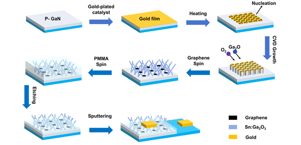
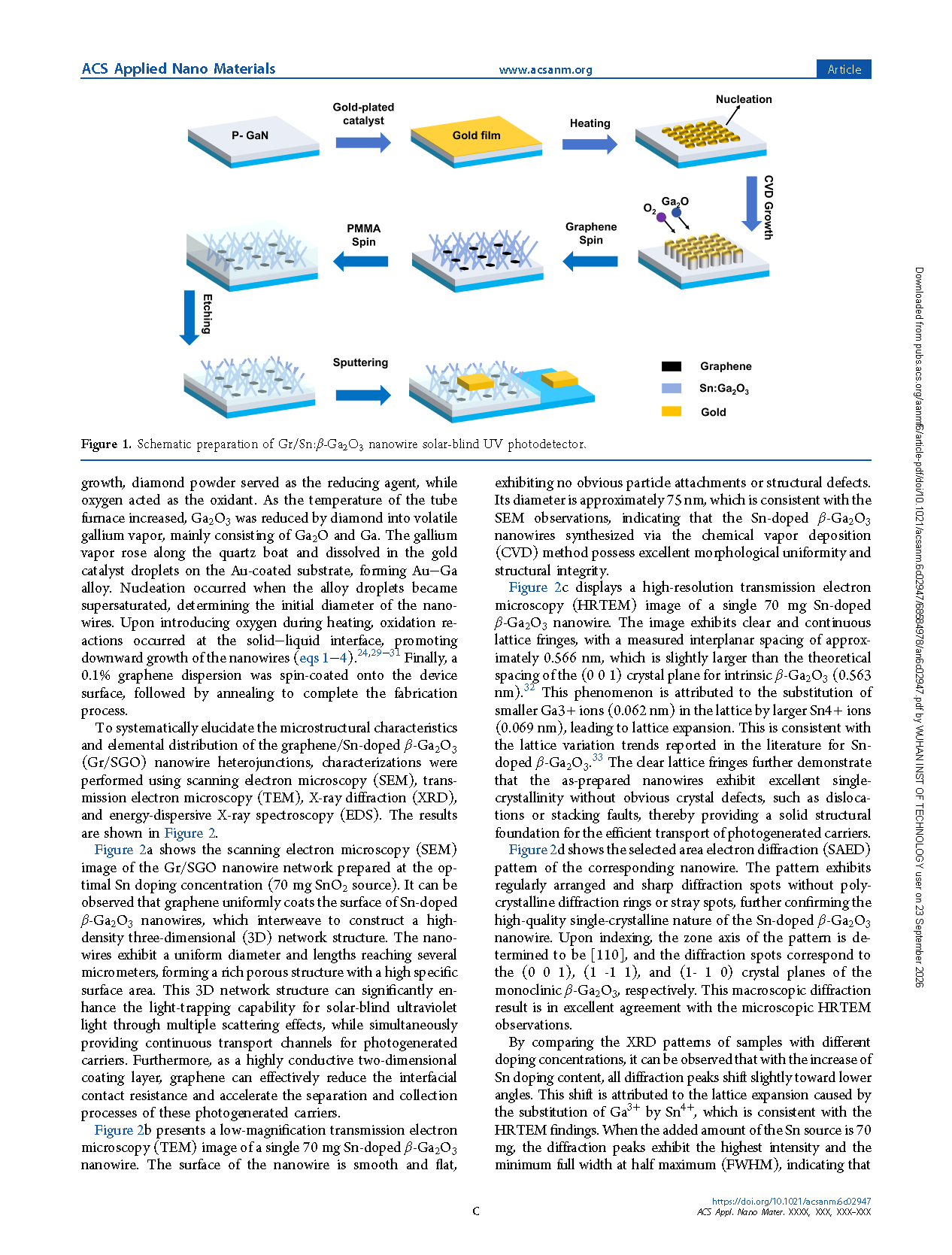
Fig. 1. Schematic preparation of Gr / Sn: β‑Ga₂O₃ nanowire solar‑blind UV photodetector.
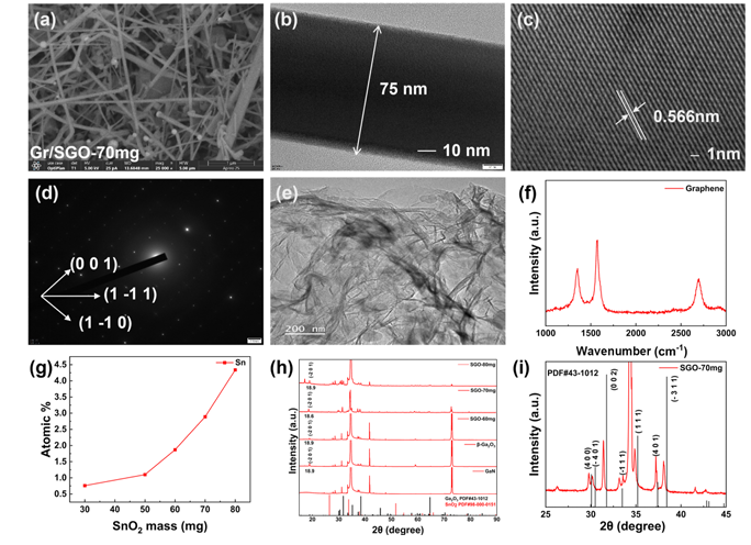
Fig. 2. (a) Scanning electron microscopy (SEM) image of the Gr/SGO‑70mg device nanowire network. (b) Transmission electron microscopy (TEM) and (c) high‑resolution transmission electron microscopy (HRTEM) images of a single SGO‑70mg nanowire. (d) Selected area electron diffraction (SAED) pattern of a single SGO‑70mg nanowire. (e) TEM image and (f) Raman spectrum of graphene. (g) Atomic percentage of the Sn element from the EDS spectrum. X‑ray diffraction (XRD) patterns of (h) the as‑prepared nanowire networks and (i) the SGO‑70 mg nanowire network.
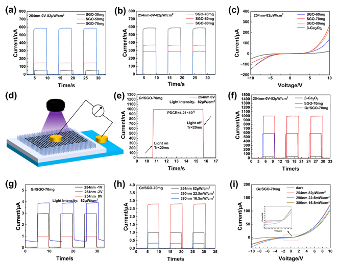
Fig. 3. (a) Comparison of the I‑t curves of Sn: β‑Ga₂O₃ with precursor SnO₂ masses of 30, 50, and 70 mg; (b) comparison of the I−t curves of Sn: β‑Ga₂O₃ with precursor SnO₂ masses of 60, 70, and 80 mg; (c) I−V curves of the devices with different precursor masses under 254 nm illumination; (d) schematic diagram of the Gr/SGO ultraviolet photodetector structure; (e) comparison of the I−t curves of the intrinsic β‑Ga₂O₃, SGO‑70mg, and Gr/SGO‑70mg devices under 254 nm illumination; (f) Magnified single‑cycle I−t curve of the Gr/SGO‑70 mg device from (e); (g) I−t curves of the device at different bias voltages under 254 nm illumination; (h) I−t curves of the device under illumination of varying wavelengths; (i) I−V curves of the device under illumination of varying wavelengths.
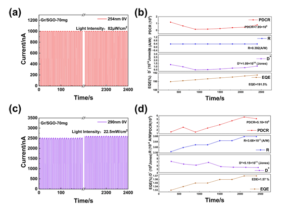
Fig. 4. (a, c) show the I‑T curves of the Gr/SGO‑70mg device after continuous operation under 254 nm and 290 nm light sources, respectively. Figure 4b,d illustrate the variation trends of the corresponding light‑to‑dark current ratio, responsivity, specific detectivity, and external quantum efficiency during this period.
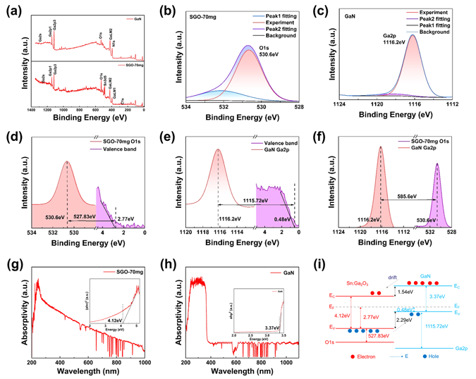
Fig. 5. (a) X‑ray photoelectron spectroscopy (XPS) survey spectra of the GaN substrate and the 70 mg‑Sn: β‑Ga₂O₃ nanowires; (b) high‑resolution O 1s spectrum of the 70 mg‑Sn: β‑Ga₂O₃ nanowires; (c) high‑resolution Ga 2p spectrum of the GaN substrate; (d) energy difference between the O1s core level and the valence band of the 70 mg‑Sn: β‑Ga₂O₃ nanowires; (e) energy difference between the Ga2p core level and the valence band of the GaN substrate; (f) binding energy difference between the O1s of the 70 mg‑Sn: β‑Ga₂O₃ nanowires and the Ga2p of the GaN substrate; (g,h) Absorption spectra of 70 mg‑Sn: β‑Ga₂O₃ and GaN, and their bandgaps calculated via Tauc plots; (i) schematic of the derived energy band alignment between them.
DOI:
doi.org/10.1021/acsanm.6c02947
Instruction
Official Account

Cooperation
Top
