


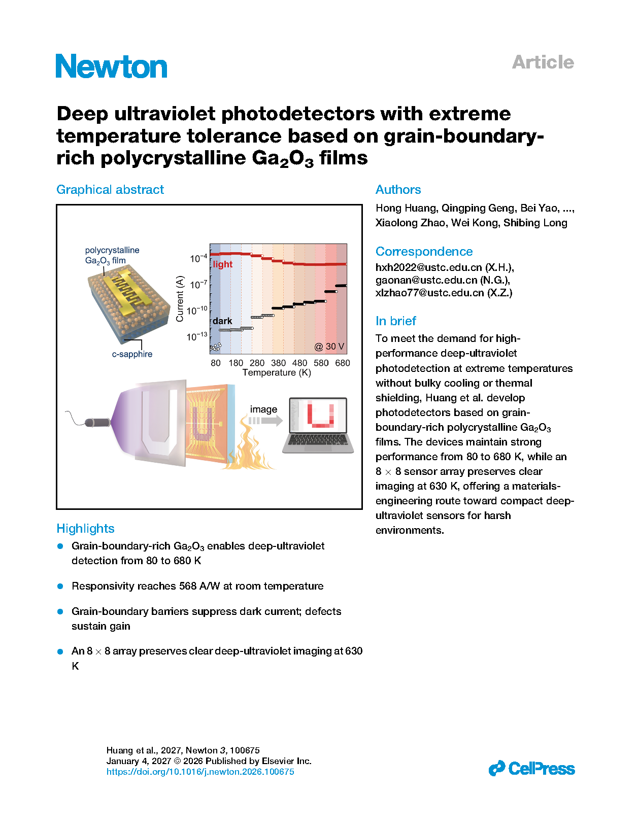
Researchers from University of Science and Technology of China, in collaboration with Westlake University, Shandong University, and the University of Hong Kong, have published a paper titled "Deep ultraviolet photodetectors with extreme temperature tolerance based on grain-boundary-rich polycrystalline Ga₂O₃ films" in the journal Newton.
Background
Deep ultraviolet (DUV) photodetection is highly valuable for flame detection, plume tracking, and deep-space exploration. But these applications often involve extreme high and low temperatures, and conventional detection systems usually depend on bulky cooling or thermal shielding. Gallium oxide (Ga₂O₃), an ultra-wide-bandgap semiconductor, offers extremely high spectral selectivity for DUV light together with excellent chemical and thermal stability, making it a promising material for solar-blind photodetectors that can withstand extreme temperatures. However, how different Ga₂O₃ microstructures and device designs perform across extreme temperatures—and the underlying physics—remains poorly understood. As a result, it is still difficult to design devices that simultaneously deliver low dark current, high gain, and high stability over a wide temperature range.
Abstract
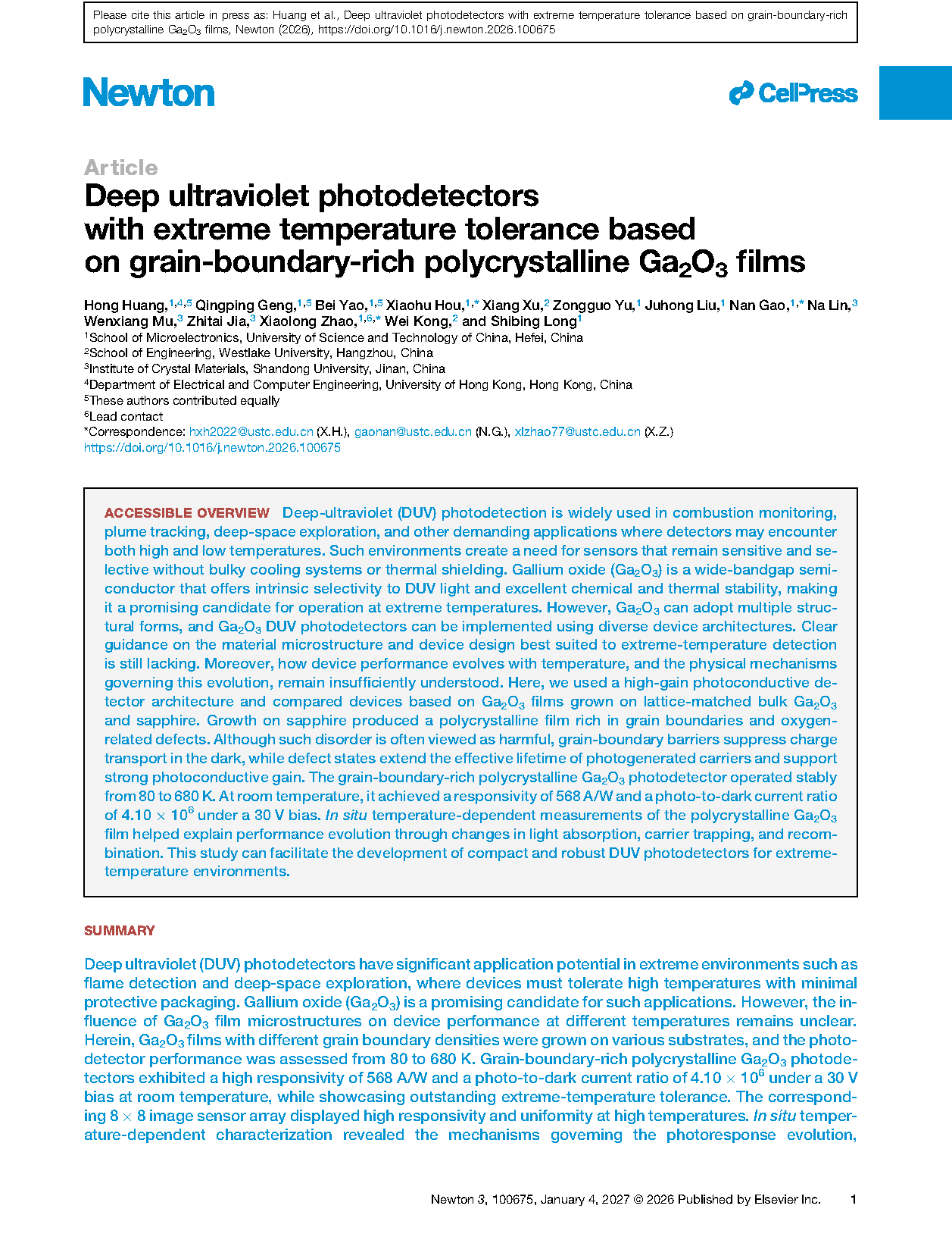
Deep-ultraviolet (DUV) photodetection is widely used in combustion monitoring, plume tracking, deep-space exploration, and other demanding applications where detectors may encounter both high and low temperatures. Such environments create a need for sensors that remain sensitive and selective without bulky cooling systems or thermal shielding. Gallium oxide (Ga₂O₃) is a wide-bandgap semi-conductor that offers intrinsic selectivity to DUV light and excellent chemical and thermal stability, making it a promising candidate for operation at extreme temperatures. However, Ga₂O₃ can adopt multiple structural forms, and Ga₂O₃ DUV photodetectors can be implemented using diverse device architectures. Clear guidance on the material microstructure and device design best suited to extreme-temperature detection is still lacking. Moreover, how device performance evolves with temperature, and the physical mechanisms governing this evolution, remain insufficiently understood. Here, we used a high-gain photoconductive detector architecture and compared devices based on Ga₂O₃ films grown on lattice-matched bulk Ga₂O₃ and sapphire. Growth on sapphire produced a polycrystalline film rich in grain boundaries and oxygen- related defects. Although such disorder is often viewed as harmful, grain-boundary barriers suppress charge transport in the dark, while defect states extend the effective lifetime of photogenerated carriers and support strong photoconductive gain. The grain-boundary-rich polycrystalline Ga₂O₃ photodetector operated stably from 80 to 680 K. At room temperature, it achieved a responsivity of 568 A/W and a photo-to-dark current ratio of 4.10 ×10⁶ under a 30 V bias. In situ temperature-dependent measurements of the polycrystalline Ga₂O₃ film helped explain performance evolution through changes in light absorption, carrier trapping, and recombination. This study can facilitate the development of compact and robust DUV photodetectors for extreme- temperature environments.
Conclusion
The DUV photodetector and imaging sensor array based on heterogeneously grown, grain-boundary-rich β-Ga₂O₃ films exhibit exceptional photoresponse performance over a wide temperature range, providing a distinct competitive edge over contemporary DUV photodetectors and facilitating the realization of reliable sensing in extreme scenarios. Temperature-dependent material characterizations reveal the mechanisms governing the temperature-induced evolution of the photoresponse, high lighting the critical influence of the microstructure and defect states on device performance. Overall, this study provides a generalizable strategy for developing compact and thermally robust DUV photodetector systems based on wide-bandgap semiconductors via tailored material engineering.
Project Support
This work was supported by the National Key Research and Development Program of China under grant nos. 2023YFB3610200 and 2024YFA1208800, the National Natural Science Foundation of China under grant nos. 62304215 and 62171426, the National Natural Science Foundation of Anhui Province under grant no. 2508085MF145, and the funding support from the University of Science and Technology of China under grant no. WK2100000056. This work was partially carried out at the Center for Micro and Nanoscale Research and Fabri cation of the University of Science and Technology of China.
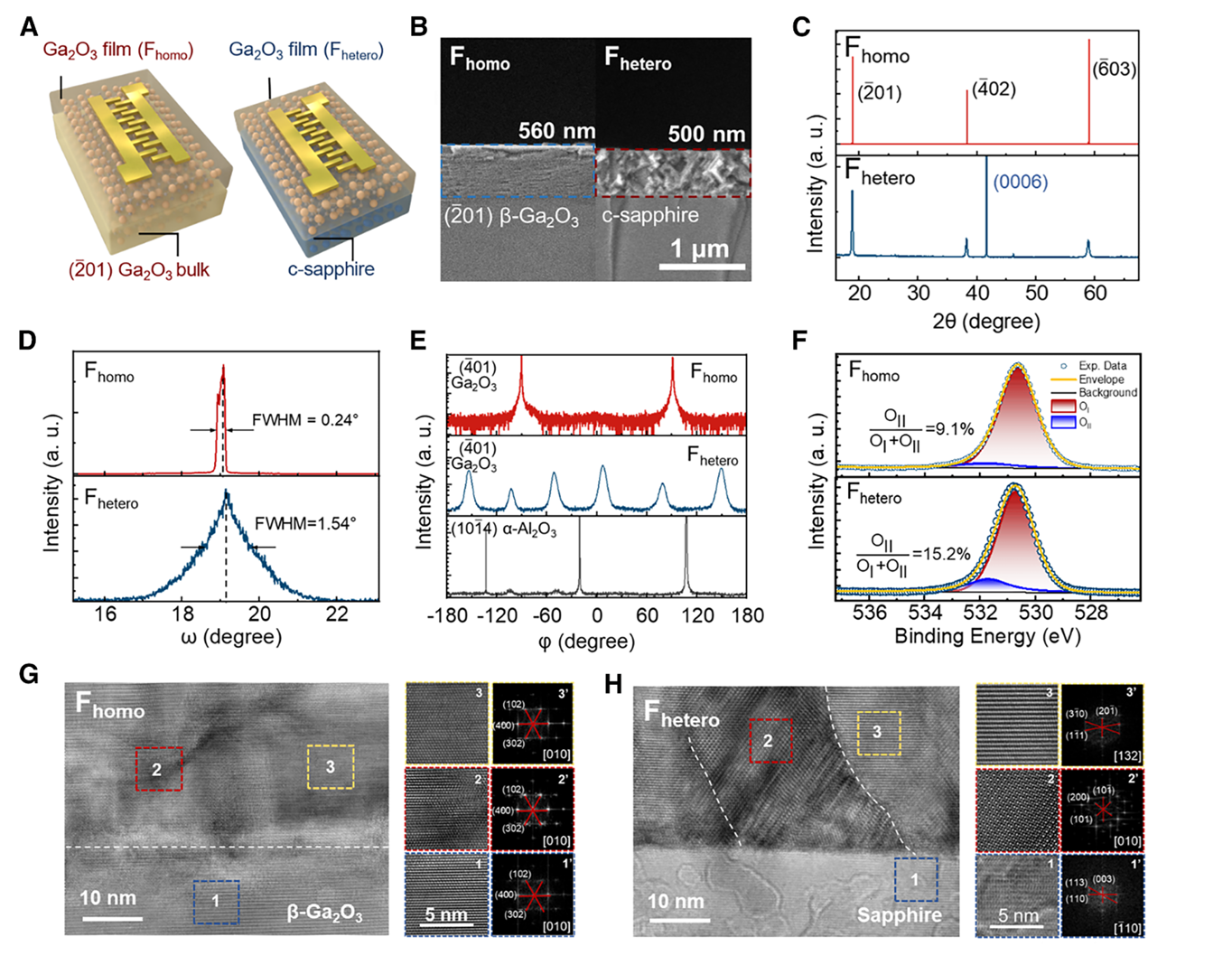
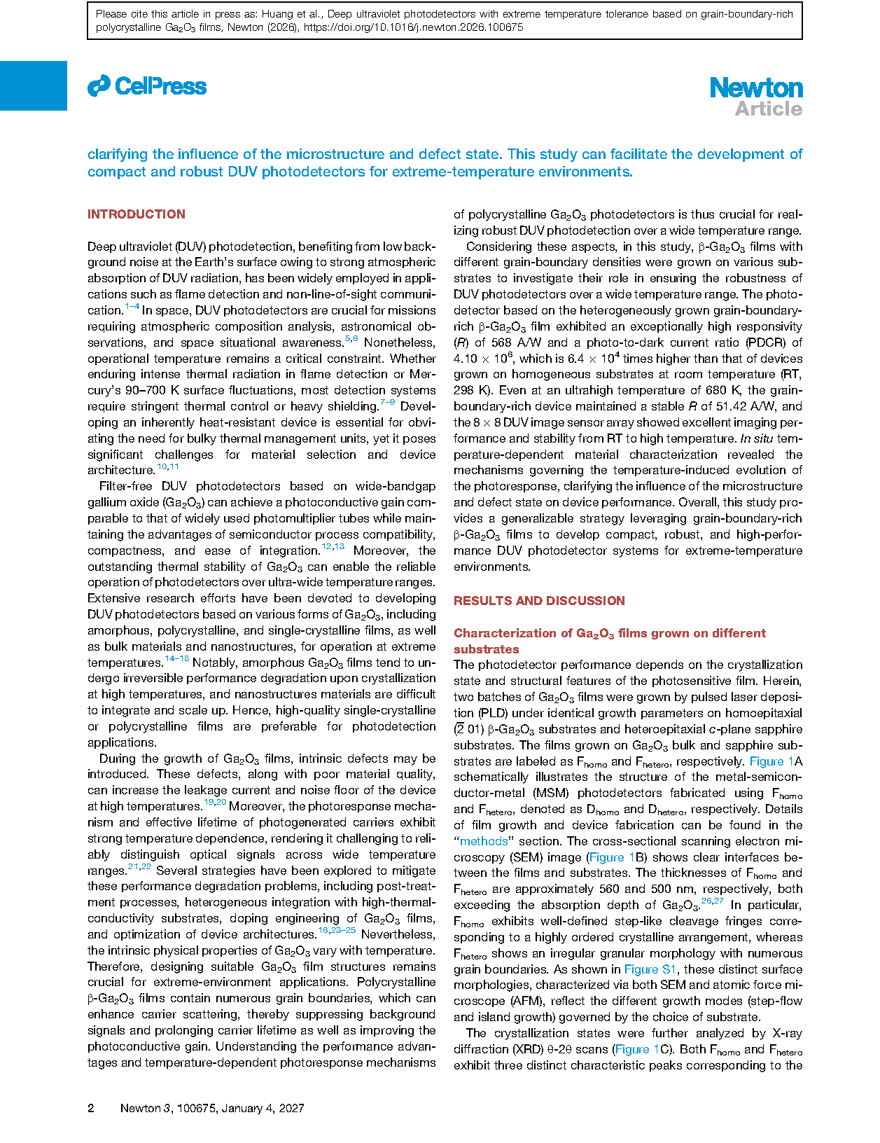
Figure 1. Comparison of material characteristics of Ga₂O₃ films grown on different substrates. (A) Schematic of the Ga₂O₃ photodetector constructed on homoepitaxial and heteroepitaxial substrates. (B–D) SEM cross-sectional images (B), XRD 2θ scans (C), and rocking curves (D) of Ga₂O₃ films grown on bulk Ga₂O₃ (Fhomo) and sapphire substrate (Fhetero). (E) XRD φ-scans of the (-4 01) reflection of the Fhomo and Fhetero Ga₂O₃ films and (10-1 4) reflections of the sapphire substrate. (F) O 1s core-level XPS spectra of the grown Ga₂O₃ films. (G and H) The cross-sectional HRTEM images for (G) Fhomo and (H) Fhetero, respectively. Magnified views of the typical regions with their corresponding FFT marked by numbers and dashed boxes are shown on the right.
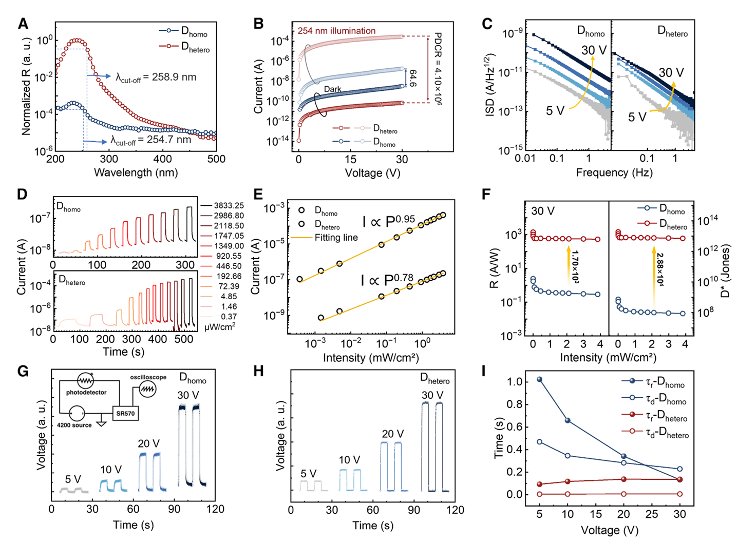
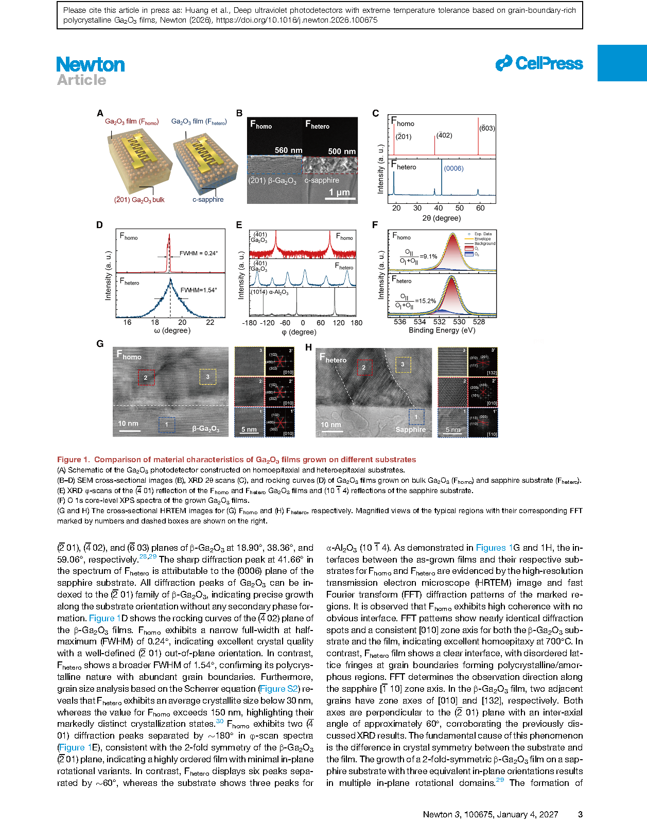
Figure 2. Photoresponse performance of Ga₂O₃ photodetectors at RT (A) Spectral response of Dhomo and Dhetero photodetectors. (B) I-V curves of Dhomo and Dhetero under 254 nm DUV illumination with a light intensity of 2.118 mW/cm2 and in dark conditions. (C) Noise spectral density of Dhomo and Dhetero at bias voltages of 5, 10, 20, and 30 V. (D) I-t curves of Dhomo and Dhetero under 254 nm illumination at various light intensities. (E) Dependence of Iphoto on light intensity.(F) R and D* as functions of voltage. (G and H) Time-dependent responses of Dhomo (G) and Dhetero (H) under different biases. (I) τr and τd of Dhomo and Dhetero under different bias.
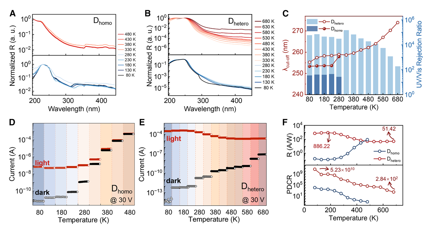
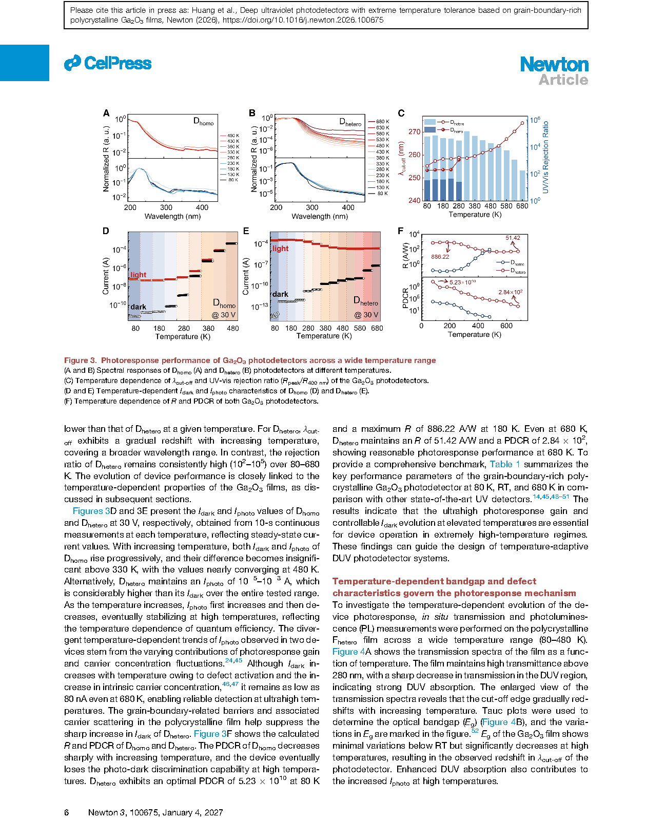
Figure 3. Photoresponse performance of Ga₂O₃ photodetectors across a wide temperature range. (A and B) Spectral responses of Dhomo (A) and Dhetero (B) photodetectors at different temperatures. (C) Temperature dependence of λcut-off and UV-vis rejection ratio (Rpeak/R400 nm) of the Ga₂O₃ photodetectors. (D and E) Temperature-dependent Idark and Iphoto characteristics of Dhomo (D) and Dhetero (E). (F) Temperature dependence of R and PDCR of both Ga₂O₃ photodetectors.
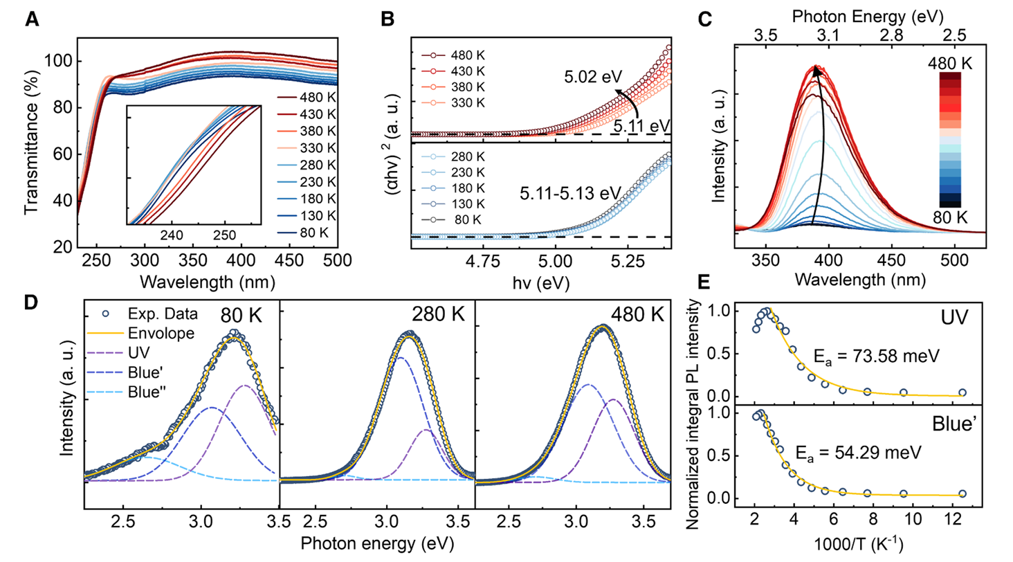
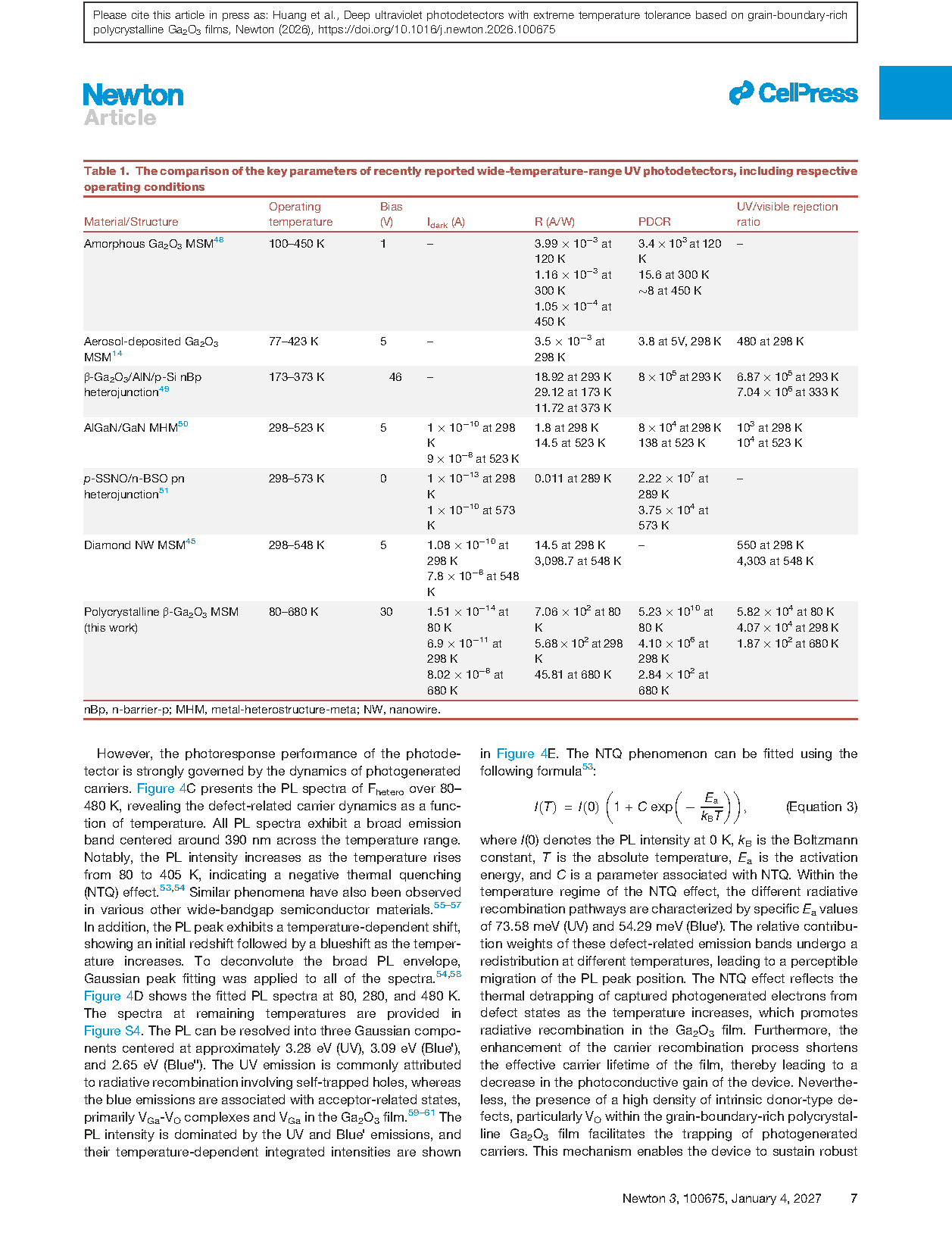
Figure 4. Bandgap shift and defect characteristics govern the Dhetero performance at different temperatures. (A) Transmission spectra as a function of temperature, with the inset showing the magnified view of the absorption edge. (B) Tauc plots of Fhetero Ga₂O₃ films at different temperatures. (C) Temperature-dependent PL spectra of the polycrystalline Ga₂O₃ film. (D) Fitted PL spectra of the polycrystalline Ga₂O₃ film at 80, 280, and 480 K. (E) Temperature-dependent integrated PL intensities of UV and Blueʹ emissions in the polycrystalline Ga₂O₃ film.
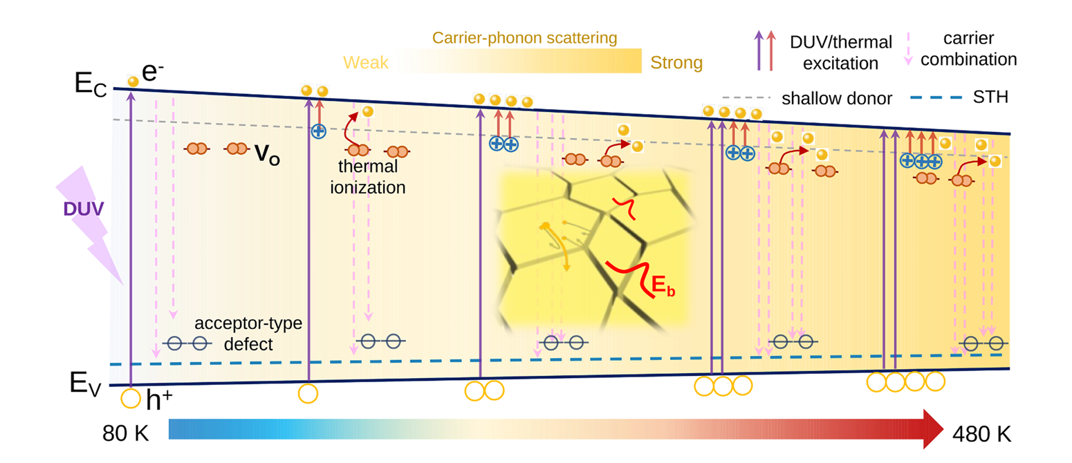
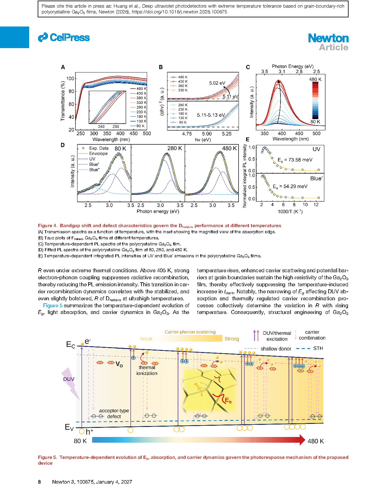
Figure 5. Temperature-dependent evolution of Eg, absorption, and carrier dynamics govern the photoresponse mechanism of the proposed device.
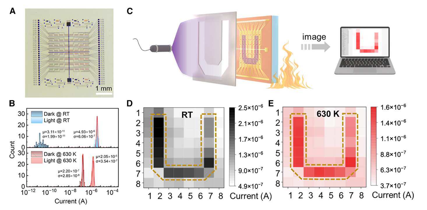
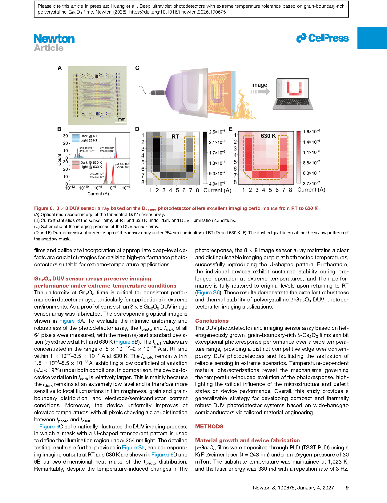
Figure 6. 8 × 8 DUV sensor array based on the Dhetero photodetector offers excellent imaging performance from RT to 630 K. (A) Optical microscope image of the fabricated DUV sensor array. (B) Current statistics of the sensor array at RT and 630 K under dark and DUV illumination conditions. (C) Schematic of the imaging process of the DUV sensor array. (D and E) Two-dimensional current maps of the sensor array under 254 nm illumination at RT (D) and 630 K (E). The dashed gold lines outline the hollow patterns of the shadow mask.
DOI:
doi.org/10.1016/j.newton.2026.100675
Instruction
Official Account

Cooperation
Top
