



Researchers from Beijing University of Technology have published a dissertation titled " Single-Photon Emitters in β-Ga₂O₃ at Distinct Excitation Energies: Defect Origin and Photophysical Properties " in Laser & Photonics Reviews.
Background
Solid-state single-photon emitters (SPEs) in wide bandgap semiconductors are currently attracting significant interest for applications in quantum communication, quantum sensing, quantum computing, and quantum key distribution, owing to their room temperature stability, broad spectral tunability, and compatibility with mature semiconductor technologies. Over the past decade, defect-based SPEs have been identified in various wide bandgap semiconductors, including diamond, SiC, GaN, hexagonal boron nitride (h-BN), AlN, and ZnO. As an emerging ultra-wide bandgap semiconductor, beta-phase gallium oxide (β-Ga₂O₃) possesses numerous excellent properties and shows great promise for next- generation electronic devices. Importantly, its large direct bandgap of ∼ 5 eV can host deep-level luminescent centers, making it a promising candidate for robust SPEs. More recently, room-temperature photostable single-photon emission has been demonstrated in β-Ga₂O₃, opening up new directions for research into solid-state SPEs.
Abstract
Room-temperature single-photon emission in beta-phase gallium oxide (β-Ga₂O₃) extends the application scope of this ultra-wide bandgap semiconductor beyond power electronics, opening up the possibility of using it as a quantum light source platform. However, the rich and complex defect landscape of β-Ga₂O₃ makes identifying the microscopic origins of these emitters a major challenge. Herein, by combining in situ confocal photoluminescence mapping, multi-wavelength excitation, and first-principles density functional theory calculations, we identify a new single-photon emitter (SPE) excited by blue (405 nm) light. The 405 nm-excited emitters exhibit high purity, excellent photostability, and a high Debye-Waller factor. They originate from the neutral VGaI-VOI divacancy, which differs from the previously reported 532 nm-excited one (VGaI-VOIII). The two emitter types show largely non-overlapping spatial distributions and different optical properties. Cross-excitation cycles reveal that 405 nm illumination can partially bleach the 532 nm-excited emitters via a photoionization process, while the reverse effect is much weaker. Our findings provide a clear defect origin for this new blue-excited SPE in β-Ga₂O₃ and establish a multi-wavelength strategy to discriminate distinct defect populations, paving the way for defect engineering in ultra-wide-bandgap semiconductor quantum photonics.
Conclusion
In summary, we have identified a new type of SPEs in β-Ga₂O₃ under 405 nm excitation, which is distinct from the previously reported 532 nm-excited SPEs. The 405 nm-excited SPEs in β-Ga₂O₃ exhibit excellent properties, such as high purity, linear polarization, excellent photostability, and a high Debye- Waller factor. By combining in situ confocal PL mapping, multi-wavelength excitation, and first-principles DFT calculations, we assign the neutral VGaI-VOI divacancy as the defect origin of the 405 nm-excited SPEs, whereas the 532 nm-excited ones originate from the VGaI-VOIII defect. Cross-excitation sequential cycles reveal that high-energy (405 nm) illumination can partially bleach the 532 nm-excited emitters through a photoionization mechanism, while the reverse effect is much weaker. Our findings expand the known defect-based SPEs in β-Ga₂O₃ and provide an experimental and theoretical basis for controlled defect engineering in this ultra-wide-bandgap semiconductor, establishing it as a promising platform for room-temperature integrated quantum photonics.
Project Support
This work was supported by the National Natural Science Foundation of China (62674006 and 52473268) and the National Key Research and Development Program of China (2024YFA1409702).
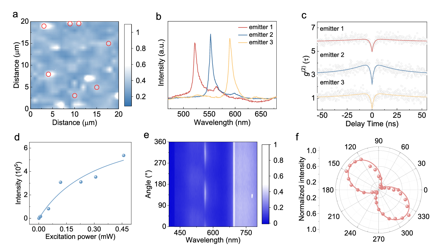
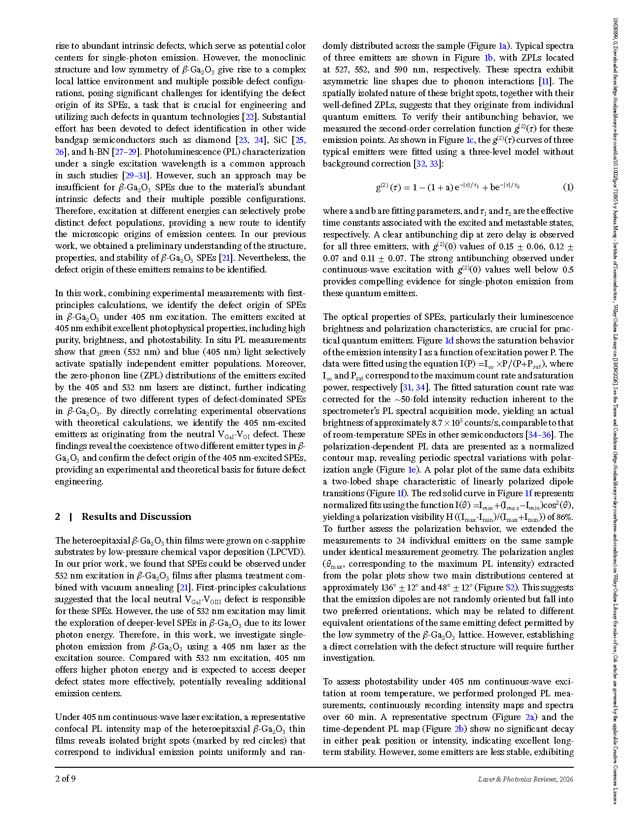
FIGURE 1 Characterization of SPEs in β-Ga₂O₃ under 405 nm excitation. (a) Representative confocal PL image of a heteroepitaxial β-Ga₂O₃ thin film. Isolated emission points are marked by red circles. (b) Representative PL spectra of three individual emitters. (c) Second-order correlation functions g(2)(τ) of the corresponding emitters measured under 0.46 mW laser excitation, exhibiting clear antibunching dips at zero delay. (d) Saturation behavior of the emission intensity as a function of excitation power, along with a theoretical fit. (e) Normalized contour map of the polarization-dependent PL data. (f) Polar plot of the PL intensity versus polarization angle θ, fitted with a cos2(θ) function (red curve).
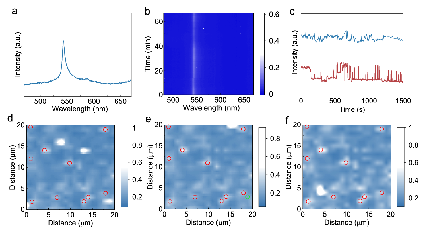
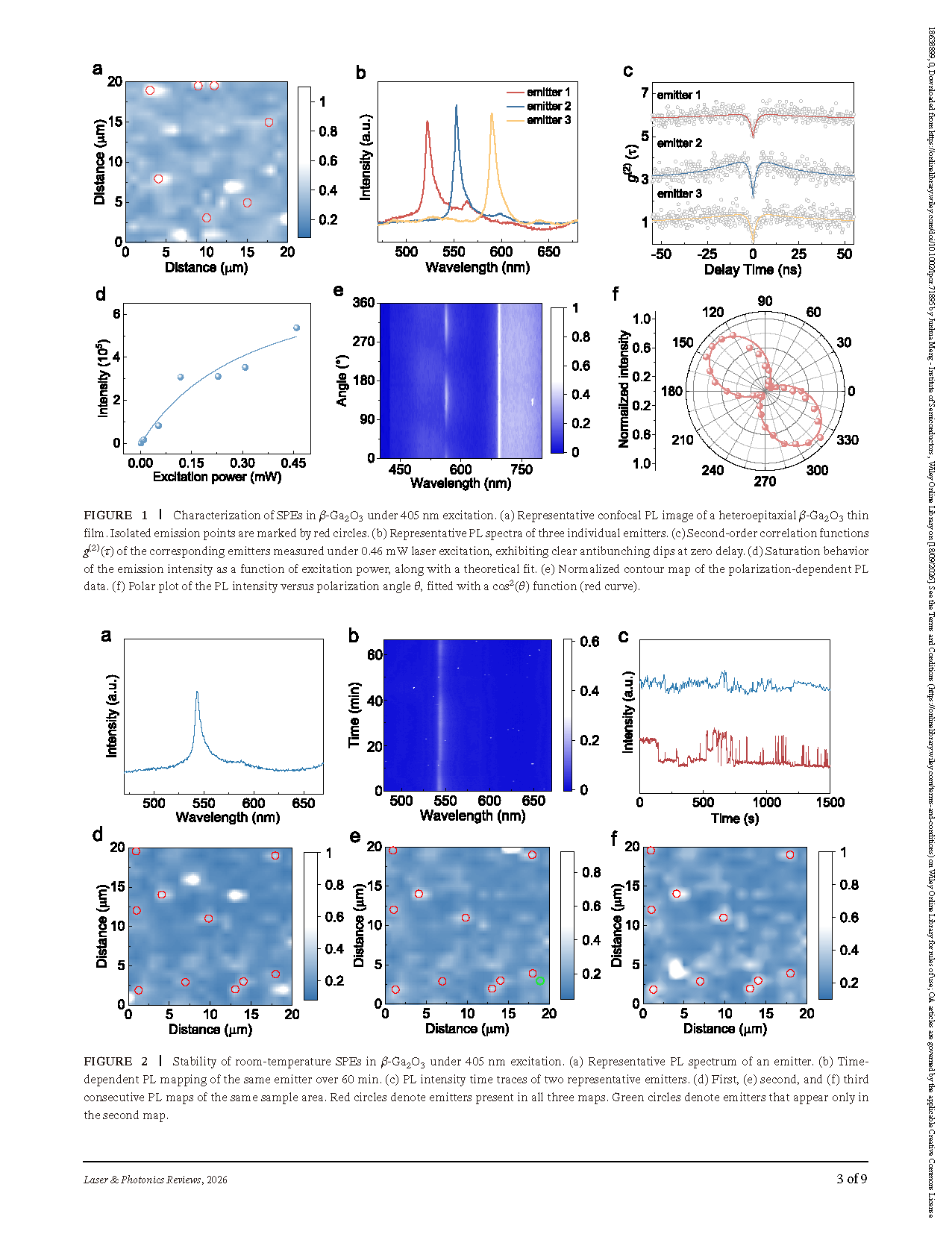
FIGURE 2 Stability of room-temperature SPEs in β-Ga₂O₃ under 405 nm excitation. (a) Representative PL spectrum of an emitter. (b) Time- dependent PL mapping of the same emitter over 60 min. (c) PL intensity time traces of two representative emitters. (d) First, (e) second, and (f) third consecutive PL maps of the same sample area. Red circles denote emitters present in all three maps. Green circles denote emitters that appear only in the second map.
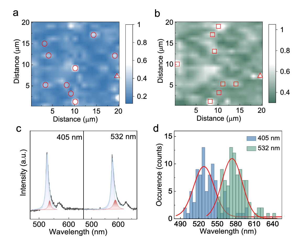
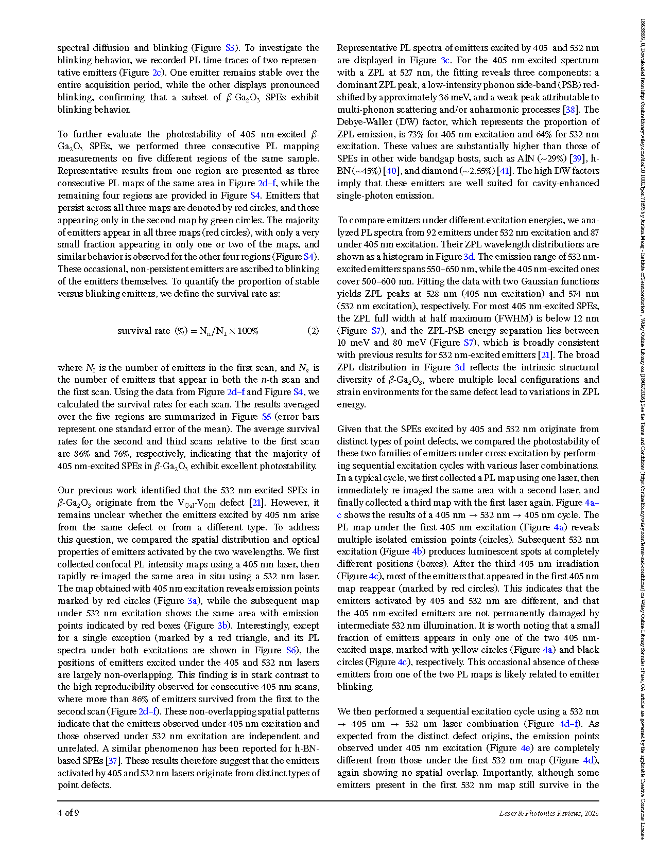
FIGURE 3 Comparison of emitters under different excitation wavelengths. (a) Confocal PL intensity map under 405 nm excitation. (b) PL intensity map of the same area recorded under 532 nm excitation. (c) Representative PL spectra of emitters excited by 405 and 532 nm. (d) Histogram of the ZPL wavelength distributions for emitters under 405 and 532 nm excitation. Red circles and boxes denote emitters observed under 405 and 532 nm excitation, respectively, while the red triangle marks the only emitter that can be excited by both wavelengths.
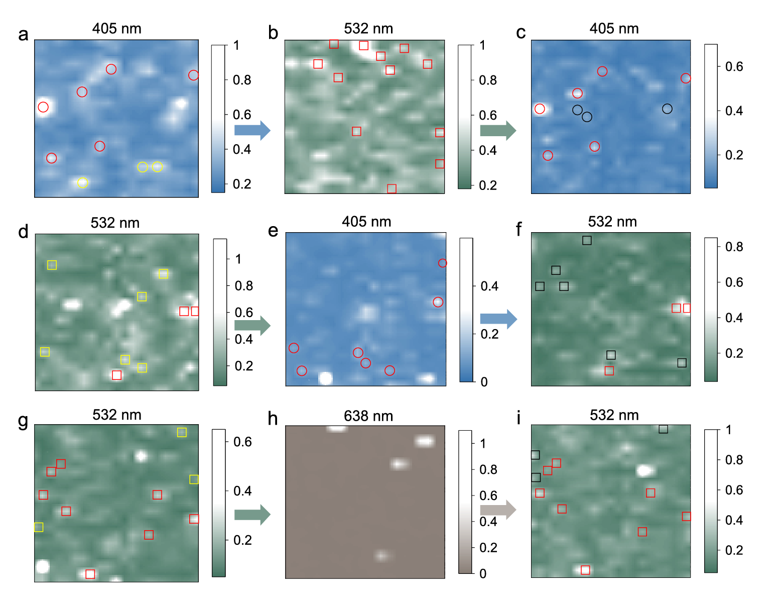
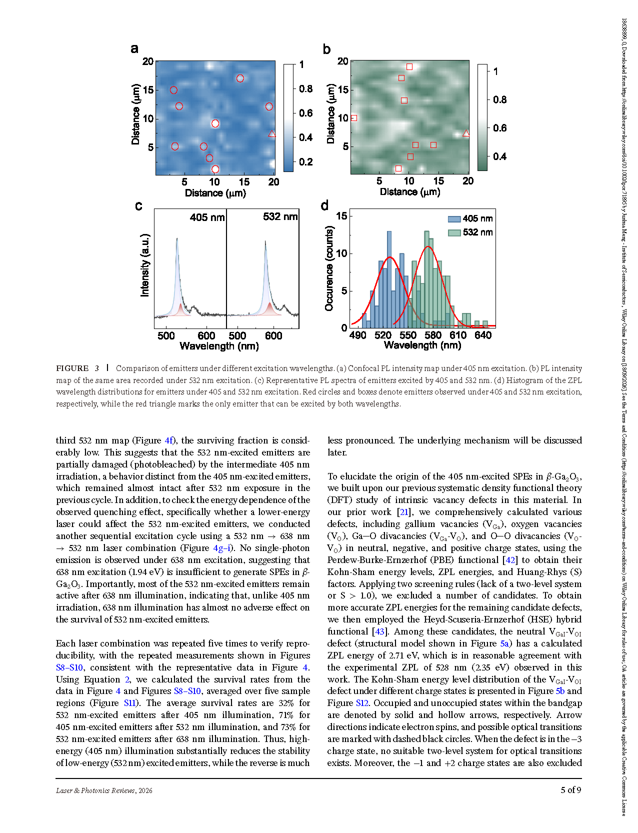
FIGURE 4 Photostability of two families of emitters under various laser combinations. (a–c) Consecutive PL maps of the same area recorded in a 405 nm → 532 nm → 405 nm cycle. (d–f) Consecutive PL maps of the same area recorded in a 532 nm → 405 nm → 532 nm cycle. (g–i) Consecutive PL maps of the same area recorded in a 532 nm → 638 nm → 532 nm cycle. PL maps acquired over a scan area of 20 × 20 µm2. In the maps, circles and squares mark emitters observed under 405 and 532 nm excitation, respectively. The colors further indicate the persistence behavior: red symbols denote emitters appearing in both the first and third scans, yellow symbols mark emitters observed only in the first scan; and black symbols correspond to emitters found solely in the third scan.
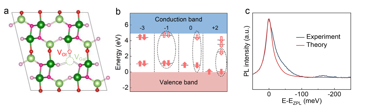
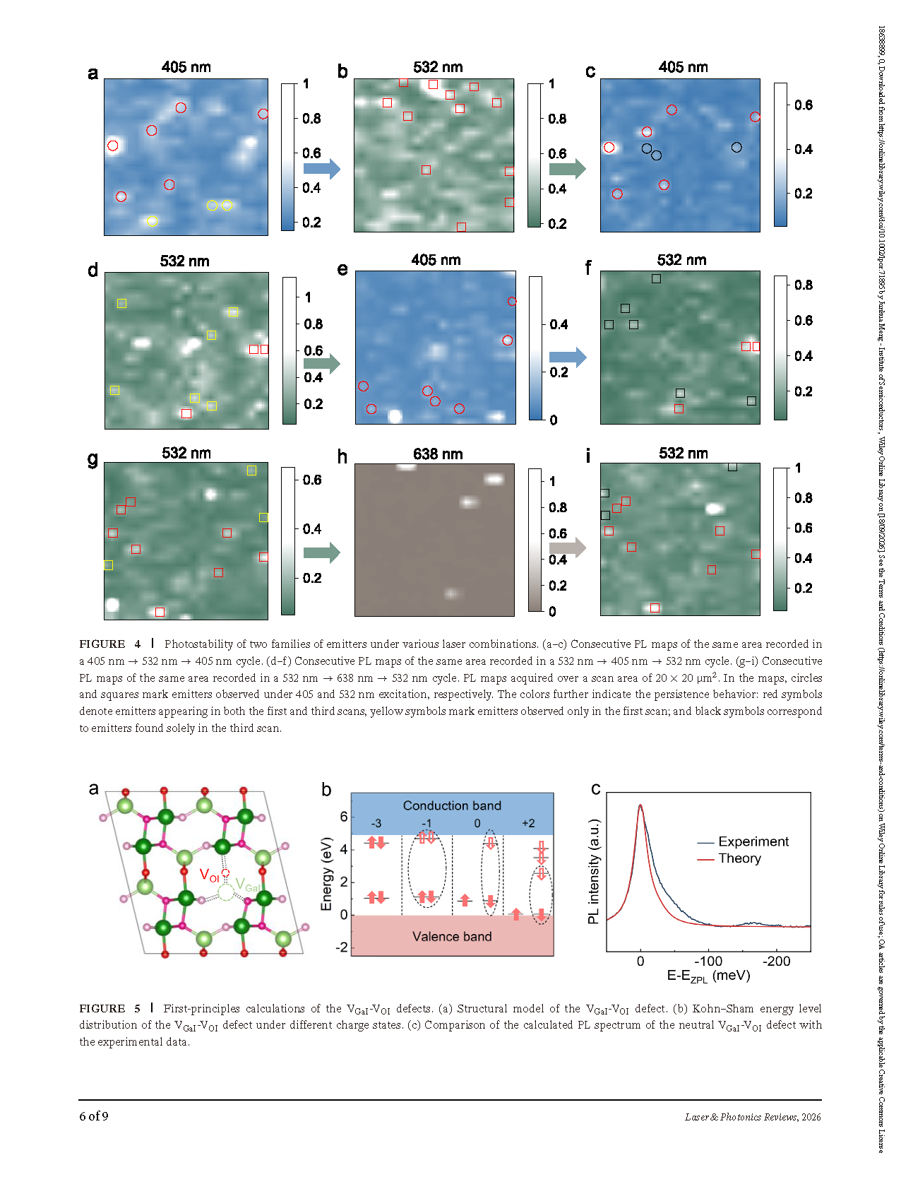
FIGURE 5 First-principles calculations of the VGaI -VOI defects. (a) Structural model of the VGaI -VOI defect. (b) Kohn–Sham energy level distribution of the VGaI -VOI defect under different charge states. (c) Comparison of the calculated PL spectrum of the neutral VGaI -VOI defect with the experimental data.
DOI:
doi.org/10.1002/lpor.71895
Instruction
Official Account

Cooperation
Top
