


Researchers from the Nanjing University, The University of Hong Kong, and Suzhou Institute of Nano-Tech and Nano-Bionics (SINANO), CAS have published a dissertation titled "Normally-Off β-Ga₂O₃ Trench-Gate Current-Aperture Vertical Electron Transistors With High-Voltage Drain-Stress Stability" in IEEE Electron Device Letters.
Background
The demand for efficient power conversion has stimulated rapid development of wide‑ and ultra‑wide bandgap power devices. Among them, β-Ga₂O₃ is attractive for power switching due to its ultra‑wide bandgap, high critical electric field, and availability of melt‑grown native substrates. However, the lack of reliable p‑type doping limits the implementation of conventional junction‑based structures for reliable electric field (E‑field) management. Over the last few years, although various vertical transistors including current‑aperture vertical electron transistors (CAVETs), FinFETs, and UMOSFETs have been demonstrated, the high‑bias reliability has not been reported.
Enhancement‑mode (E‑mode) operation is essential for fail‑safe power switching. Fin‑gate and deeply etched trench‑gate structures can effectively deplete the channel to achieve the E‑mode operation, but high‑energy plasma etching and trench‑corner field crowding have been reported to introduce severe defects and trapping, increased hysteresis, high leakage current, and compromised reliability.
On the other hand, CAVETs provide an alternative approach by using a buried current‑blocking layer (CBL) to shield the top channel region from high E‑field. Nevertheless, in planar‑gate CAVETs, E‑mode operation requires an ultrathin surface channel, the fabrication of which is strongly constrained by the narrow implantation window. To date, normally‑off β-Ga₂O₃ CAVETs with stable high‑voltage operation have rarely been reported.
Abstract
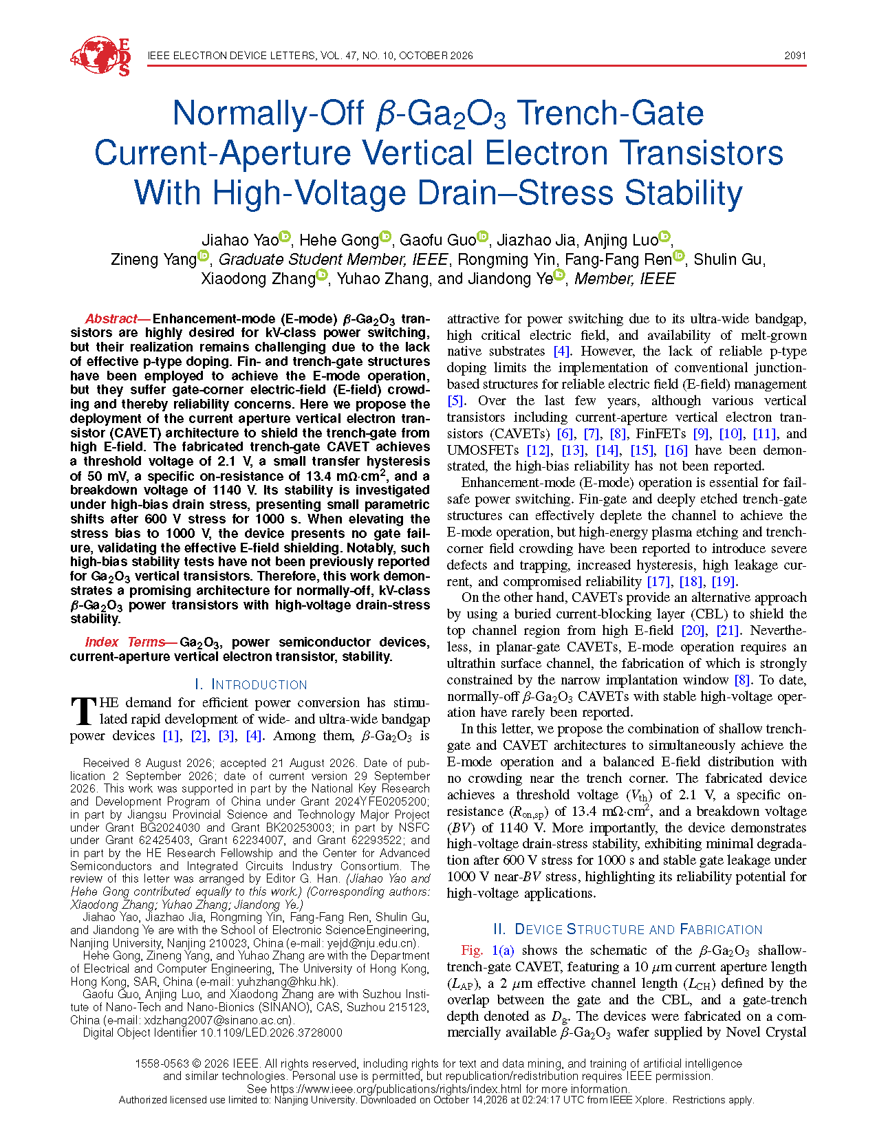
Enhancement-mode (E-mode) β-Ga₂O₃ transistors are highly desired for kV-class power switching, but their realization remains challenging due to the lack of effective p-type doping. Fin- and trench-gate structures have been employed to achieve the E-mode operation, but they suffer gate-corner electric-field (E-field) crowding and thereby reliability concerns. Here we propose the deployment of the current aperture vertical electron transistor (CAVET) architecture to shield the trench-gate from high E-field. The fabricated trench-gate CAVET achieves a threshold voltage of 2.1 V, a small transfer hysteresis of 50 mV, a specific on-resistance of 13.4 mΩ·cm², and a breakdown voltage of 1140 V. Its stability is investigated under high-bias drain stress, presenting small parametric shifts after 600 V stress for 1000 s. When elevating the stress bias to 1000 V, the device presents no gate failure, validating the effective E-field shielding. Notably, such high-bias stability tests have not been previously reported for Ga₂O₃ vertical transistors. Therefore,this work demonstrates a promising architecture for normally-off, kV-classβ-Ga₂O₃ power transistors with high-voltage drain-stress stability.
Highlights
Device innovation: shallow-trench-gate combined with CAVET architecture :The team combines shallow-trench-gate and CAVET (Current-Aperture Vertical Electron Transistor). The buried CBL (Current-Blocking Layer) relocates peak electric field away from trench-gate corners to the buried layer, mitigating field crowding while realizing normally-off operation.
Excellent static device performance :The fabricated device features a threshold voltage of 2.1 V, transfer hysteresis of 50 mV, specific on-resistance of 13.4 mΩ·cm², breakdown voltage of 1140 V and on/off current ratio of ~10⁸, showing compelling comprehensive performance among reported enhancement-mode vertical β-Ga₂O₃ devices.
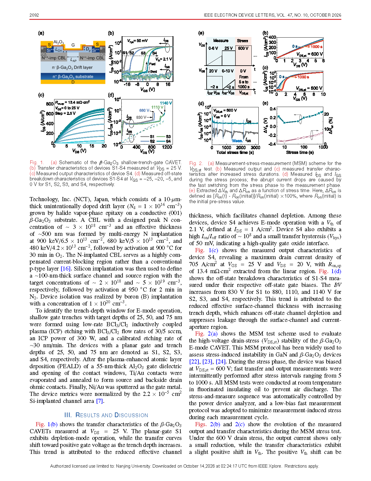
First reported high‑voltage drain‑stress reliability for vertical β-Ga₂O₃ transistors:After 600 V drain stress for 1000 s, the device exhibits ΔVₜₕ < 0.4 V and ΔRₒₙ < 8 %. No gate failure occurs under 1000 V near‑breakdown stress, demonstrating high‑voltage reliability potential.
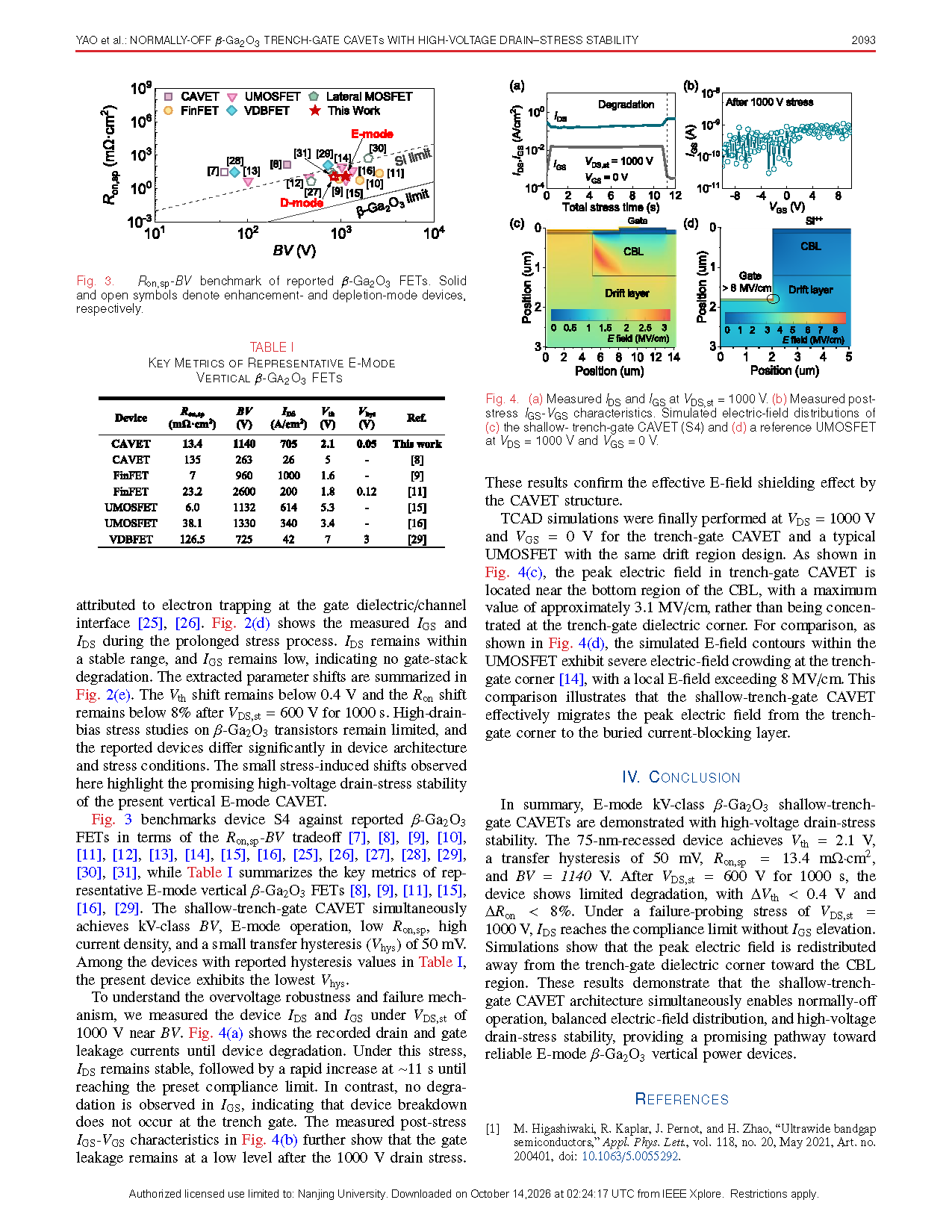
TCAD simulation verifies electric‑field shielding mechanism:TCAD (Technology Computer‑Aided Design) simulations compare electric‑field distributions between UMOSFET and the proposed device, confirming the architecture shifts peak electric‑field to buried current‑blocking layer and relieves high field stress on trench‑gate dielectrics.
Conclusion
In summary, E-mode kV-class β-Ga₂O₃ shallow-trench-gate CAVETs are demonstrated with high-voltage drain-stress stability. The 75-nm-recessed device achieves Vₜₕ = 2.1 V, a transfer hysteresis of 50 mV, Rₒₙ,ₛₚ = 13.4 mΩ·cm², and BV = 1140 V. After VDS,st=600 V for1000s,the device shows limited degradation, with ΔVₜₕ < 0.4 V and ΔRₒₙ< 8 %. Under a failure-probing stress of VDS,st=1000V, IDS reaches the compliance limit without IGS elevation. Simulations show that the peak electric field is redistributed away from the trench-gate dielectric corner toward the CBL region. These results demonstrate that the shallow-trench-gate CAVET architecture simultaneously enables normally-off operation, balanced electric-field distribution, and high-voltage drain-stress stability, providing a promising pathway toward reliable E-mode β-Ga₂O₃ vertical power devices.
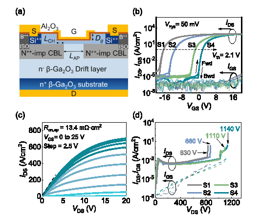
Fig. 1. (a) Schematic of the β-Ga₂O₃ shallow-trench-gate CAVET. (b) Transfer characteristics of devices S1-S4 measured at VDS=25 V. (c) Measured output characteristics of device S4. (d) Measured off-state breakdown characteristics of devices S1-S4 at VGS=-25,-20,-5, and 0 V for S1, S2, S3, and S4, respectively.
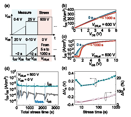
Fig. 2. (a) Measurement-stress-measurement (MSM) scheme for the VDS,st test. (b) Measured output and (c) measured transfer characteristics after increased stress durations. (d) Measured IDS and IGS during the stress process; the abrupt current drops are caused by the fast switching from the stress phase to the measurement phase. (e) Extracted ΔVₜₕ and ΔRₒₙ as a function of stress time. Here, ΔRₒₙ is defined as [Rₒₙ(t)-Rₒₙ(initial)] / Rₒₙ(initial) ×100 %, where Rₒₙ(initial) is the initial pre-stress value.
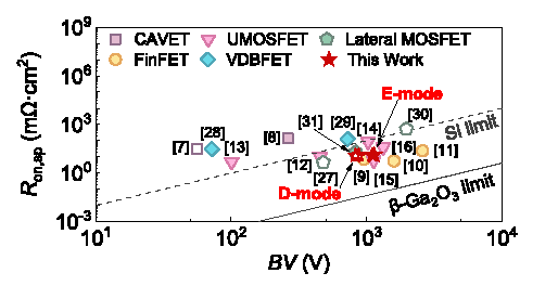
Fig. 3. Rₒₙ,ₛₚ-BV benchmark of reported β-Ga₂O₃ FETs. Solid and open symbols denote enhancement- and depletion-mode devices, respectively.
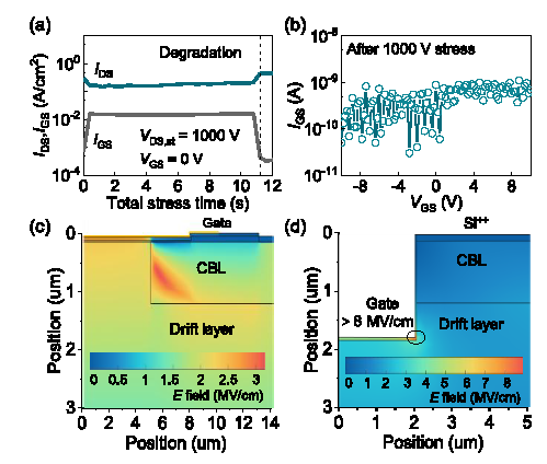
Fig. 4. (a) Measured IDS and IGS at VDS,st=1000 V (b) Measured post-stress IGS-VGS characteristics. Simulated electric-field distributions of (c) the shallow-trench-gate CAVET (S4) and (d) a reference UMOSFET at VDS=1000 V and VGS=0 V.
DOI:
10.1109/LED.2026.3728000
Instruction
Official Account

Cooperation
Top
