


Researchers from the Xidian University have published a dissertation titled "3.23 GW/cm² power figure of merit and 0.69 V turn-on voltage β-Ga₂O₃ heterojunction barrier Schottky diodes with p-i-n junction termination " in Science China-Information Sciences.
Background
Owing to its ultrawide bandgap and high critical breakdown electric field, β-Ga₂O₃ holds great potential for high-voltage power electronic devices. However, the lack of reliable p-type β-Ga₂O₃ restricts the development of high-performance homojunction bipolar devices. Accordingly, fabricating heterojunctions between p-type oxides (especially NiOₓ) and n-type β-Ga₂O₃ has become a feasible approach to boost device performance. For β-Ga₂O₃ heterojunction barrier Schottky (HJBS) diodes, an inherent trade-off exists between breakdown voltage (BV) and turn-on voltage (Vₒₙ): improving voltage blocking capability generally requires a higher effective barrier height, which inevitably increases forward conduction loss. To address this dilemma, acceptor doping is proposed to modulate the Fermi level for enhanced blocking capability without a substantial rise in Vₒₙ. Nitrogen (N) doping has been proven to form a current-blocking layer in β-Ga₂O₃ devices. Moreover, theoretical calculations reveal that co-doping with two impurities enables more efficient electronic-structure modulation than single-impurity doping. Inspired by these findings, this work incorporates a p-i-n junction termination structure realized via N/P co-doping in NiOₓ/β-Ga₂O₃ HJBS diodes. Together with a p-NiOₓ termination ring, this design creates an internal junction with charge-compensation effects at the anode edge. Such a structure tailors the local electric field distribution and mitigates edge electric field crowding. As a result, the breakdown voltage is improved while low forward Vₒₙ and on-resistance (Rₒₙ) are maintained, achieving synergistic enhancement of voltage blocking capability and conduction efficiency.
Abstract
β-Ga2O3 has attracted extensive interest for high-voltage power electronics owing to its ultra-wide bandgap and high critical electric field. However, the lack of reliable p-type β-Ga2O3 fundamentally restricts the realization of high-performance bipolar devices. Heterojunction structures employing p-type oxides,particularly NiOx, provide a feasible pathway, yet they often suffer from a trade-off between breakdown voltage(BV) and turnon voltage(Von).
Conclusion
In summary, NiO/β-Ga₂O₃ HJBS diodes incorporating an N/P co-doped p-i-n termination were demonstrated. The compensated implantation region effectively enhances voltage blocking capability while preserving low forward conduction loss. The devices achieve a BV of 3.9 kV and an Ron,sp of 4.75 mΩ·cm², corresponding to a P-FOM of 3.23 GW/cm². Additionally, stable electrical characteristics up to 150°C indicate robust thermal performance. These results provide an effective strategy for simultaneously improving breakdown capability and conduction efficiency in β-Ga₂O₃ power devices.
Project Support
This work was supported by National Natural Science Foundation of China (Grant Nos. 62222407, 62421005) and Guangdong Basic and Applied Basic Research Foundation (Grant No. 2023B1515040024).
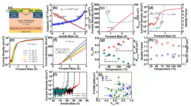
Figure 1 (a) Schematic image of the cross-sectional vertical β-NiO/Ga2O3 HJBS diodes with N/P ion implantation. (b) Measured C–V and extracted 1/C2 –V curves of Ga2O3 HJBS diodes with a radius of 150 µm. (c) Linear-scale J–V curves and log-scale Ron,sp. (d) Log-scale J–V characteristics and the extracted ideality factors. (e) Log-scale and (f) linear-scale T-dependent JF –VF curves measured in steps of 25°C from 25°C to 150°C. (g) Extracted Von and Ron,sp versus temperature from 25°C to 150°C. (h) T-dependent ideality factor and barrier height characteristics at T ranging from 25°C to 150°C. (i) Breakdown characteristics for devices in this work (solid lines) and devices fabricated without ion-implanted termination (dashed lines). (j) Von versus P-FOM benchmark plot comparing our Ga2O3 HJBS diodes and other state-of-the-art Ga2O3 SBDs and JBS diodes.
DOI:
doi.org/10.1007/s11432-025-4862-4
Instruction
Official Account

Cooperation
Top