


Researchers from the Air Force Research Laboratory have published a dissertation titled "Spatially resolved heavy ion microprobe testing of lateral Ga₂O₃ MOSFETs" in Applied Physics Letters.
Background
β-Ga2O3 has been heavily researched over the past decade for next-generation power electronics applications due to its ultrawide bandgap combined with mature liquid-phase bulk crystal growth, facile homoepitaxy, and dopability. Potential space applications of β-Ga2O3 are particularly valuable due to the established susceptibility of SiC and GaN to single event burnout effects due to heavy ion collisions.
There is insufficient investigation to determine the capability of β-Ga2O3 electronics for space applications. Manikanthababu et al. report an increase in leakage current correlated with chemical changes for vertical Ga2O3 Schottky diodes under 120 MeV Ag7+ ion irradiation. Cadena et al. and Islam et al. demonstrate single event burnout in vertical Ga2O3 Schottky diodes. Ma et al. simulated the influence of heavy ion irradiation on β-Ga2O3 MOSFETs, finding that the gate corner near the drain side is the most sensitive location for a single event effect. Zhai et al. report increased leakage current and decreased breakdown voltage of Al2O3/β-Ga2O3 metal-oxide-semiconductor capacitors (MOSCAPs) post heavy ion Ta irradiation.
Abstract
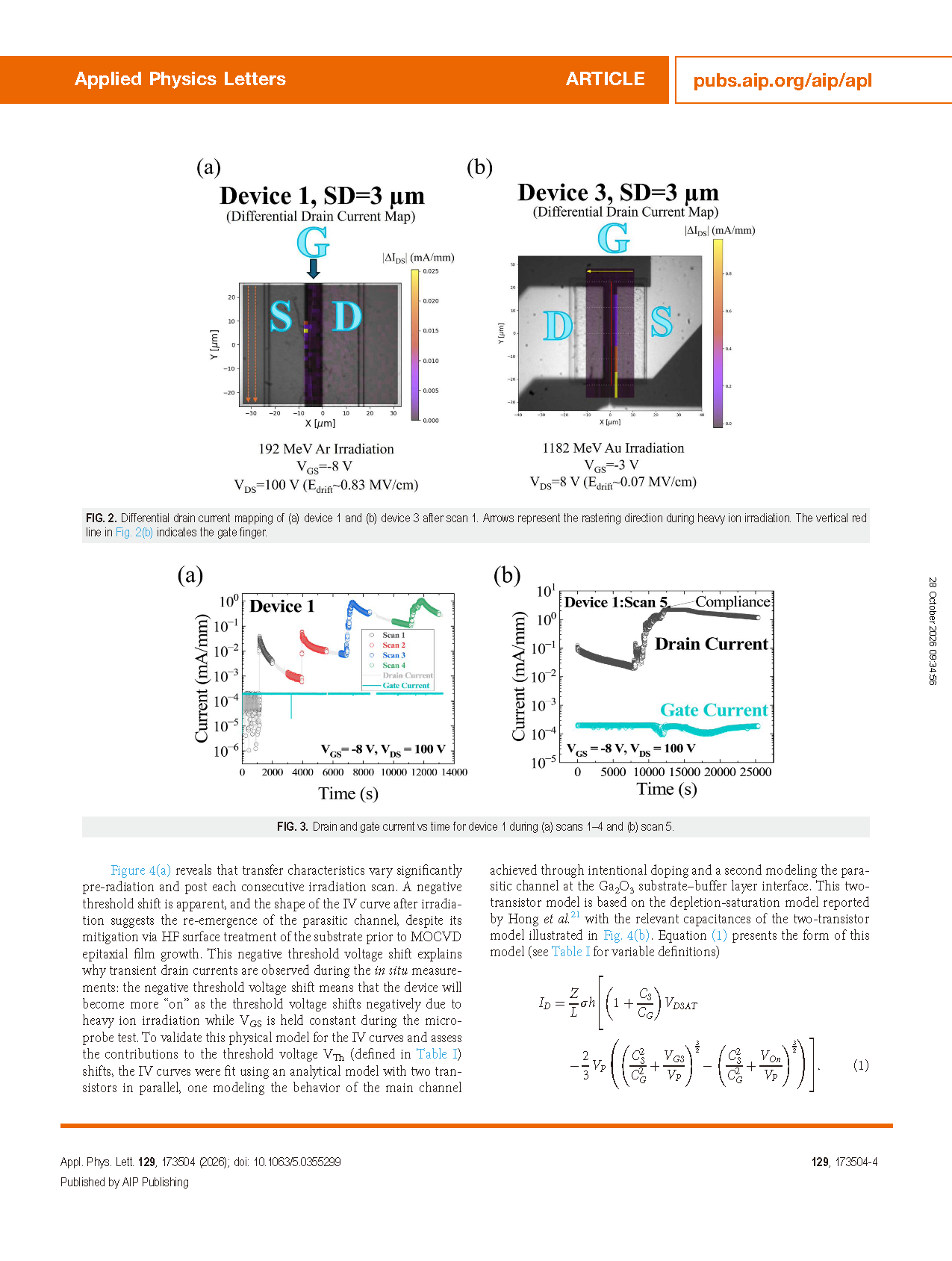
Ultrawide bandgap β-Ga2O3 has been intensively researched for power electronics applications after the first demonstration of high quality MOSFETs and MESFETs in 2012. Testing of β-Ga2O3 transistor structures under heavy ion irradiation is relatively unexplored despite its criticality in developing next-generation radiation-hardened electronics for space applications. Single ion irradiation was performed with 192 MeV Ar and 1182 MeV Au and a lateral spatial resolution of ∼0.5 μm to map the electrical characteristics of β-Ga2O3 MOSFETs as a function of irradiation position and identify the most sensitive regions of the device. This work determines that standard Ga2O3 MOSFETs are not susceptible to single event burnout under in operando irradiation under an applied field of 0.83 MV/cm for Ar irradiation as well as an applied field of 0.07 MV/cm for Au irradiation. Successive irradiations reveal transient increases in drain current associated with threshold voltage shifts attributed to defect generation/ionization in the top atomic layer deposited-Al2O3 dielectric or the semi-insulating Ga2O3 substrate and subsequent thermal relaxation. Fitting in situ transfer curve data reveals that the dominant effect under heavy ion irradiation is the activation of the parasitic channel via the generation of net positive charge at the buffer–substrate interface.
Highlights
Spatially resolved current response measurements were achieved for lateral Ga₂O₃MOSFETs during single-ion irradiation, revealing that the channel region exhibits significant sensitivity to the ion impact location.
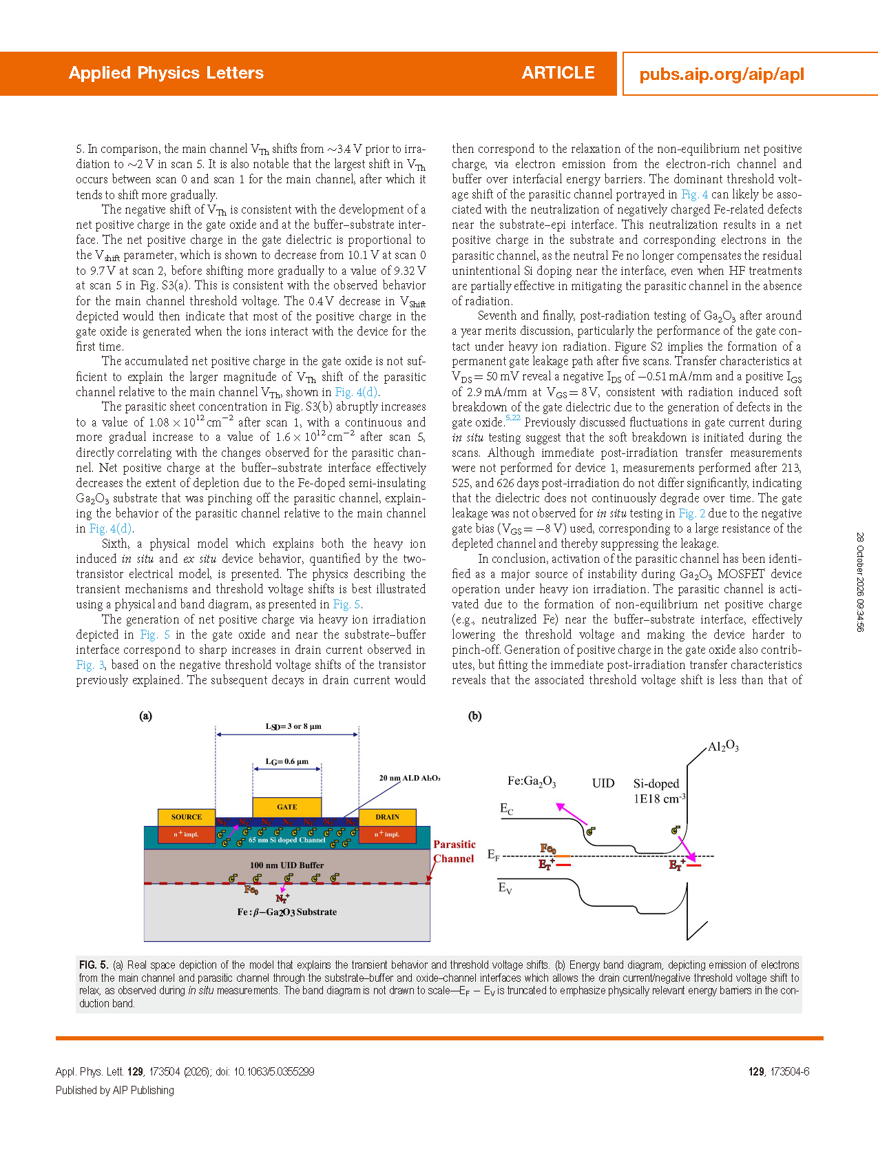
By fitting the transfer characteristics before and after irradiation using a dual-transistor model, we distinguished the changes in threshold voltage between the main channel and the parasitic channel, demonstrating that the threshold voltage drift in the parasitic channel is more pronounced than that in the main channel, and is a significant source of electrical instability in the device following irradiation.
It was found that heavy-ion irradiation may also lead to the formation of permanent leakage paths in the gate dielectric, indicating that gate dielectric reliability and the control of parasitic channels at the buffer-substrate interface are two key areas for enhancing the radiation resistance of Ga₂O₃ MOSFETs.
Conclusion
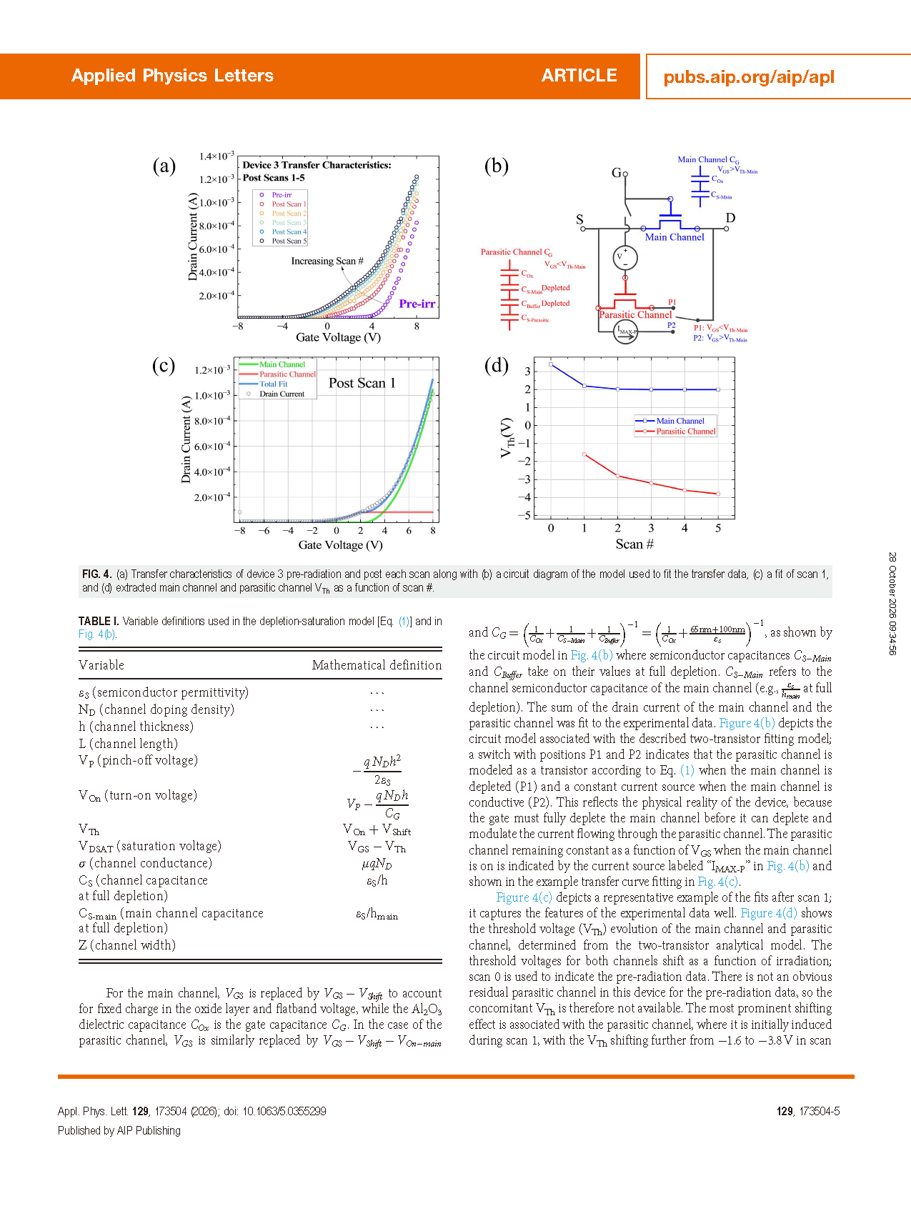
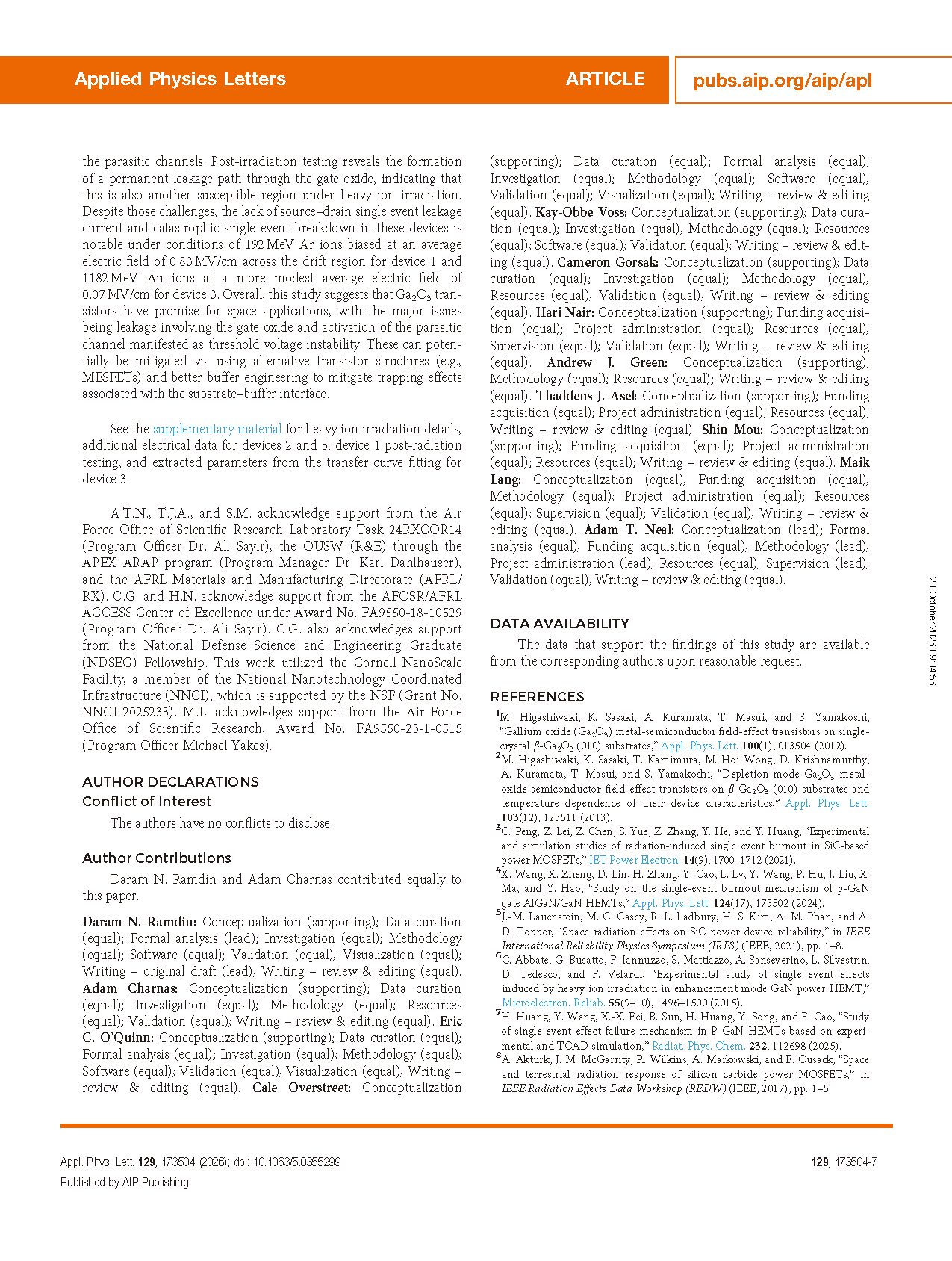
In conclusion, activation of the parasitic channel has been identified as a major source of instability during Ga2O3 MOSFET device operation under heavy ion irradiation. The parasitic channel is activated due to the formation of non-equilibrium net positive charge (e.g., neutralized Fe) near the buffer–substrate interface, effectively lowering the threshold voltage and making the device harder to pinch-off. Generation of positive charge in the gate oxide also contributes, but fitting the immediate post-irradiation transfer characteristics reveals that the associated threshold voltage shift is less than that of the parasitic channels. Post-irradiation testing reveals the formation of a permanent leakage path through the gate oxide, indicating that this is also another susceptible region under heavy ion irradiation. Despite those challenges, the lack of source–drain single event leakage current and catastrophic single event breakdown in these devices is notable under conditions of 192 MeV Ar ions biased at an average electric field of 0.83 MV/cm across the drift region for device 1 and 1182 MeV Au ions at a more modest average electric field of 0.07 MV/cm for device 3. Overall, this study suggests that Ga2O3 transistors have promise for space applications, with the major issues being leakage involving the gate oxide and activation of the parasitic channel manifested as threshold voltage instability. These can potentially be mitigated via using alternative transistor structures (e.g., MESFETs) and better buffer engineering to mitigate trapping effects associated with the substrate–buffer interface.
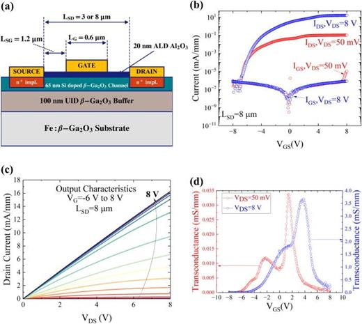
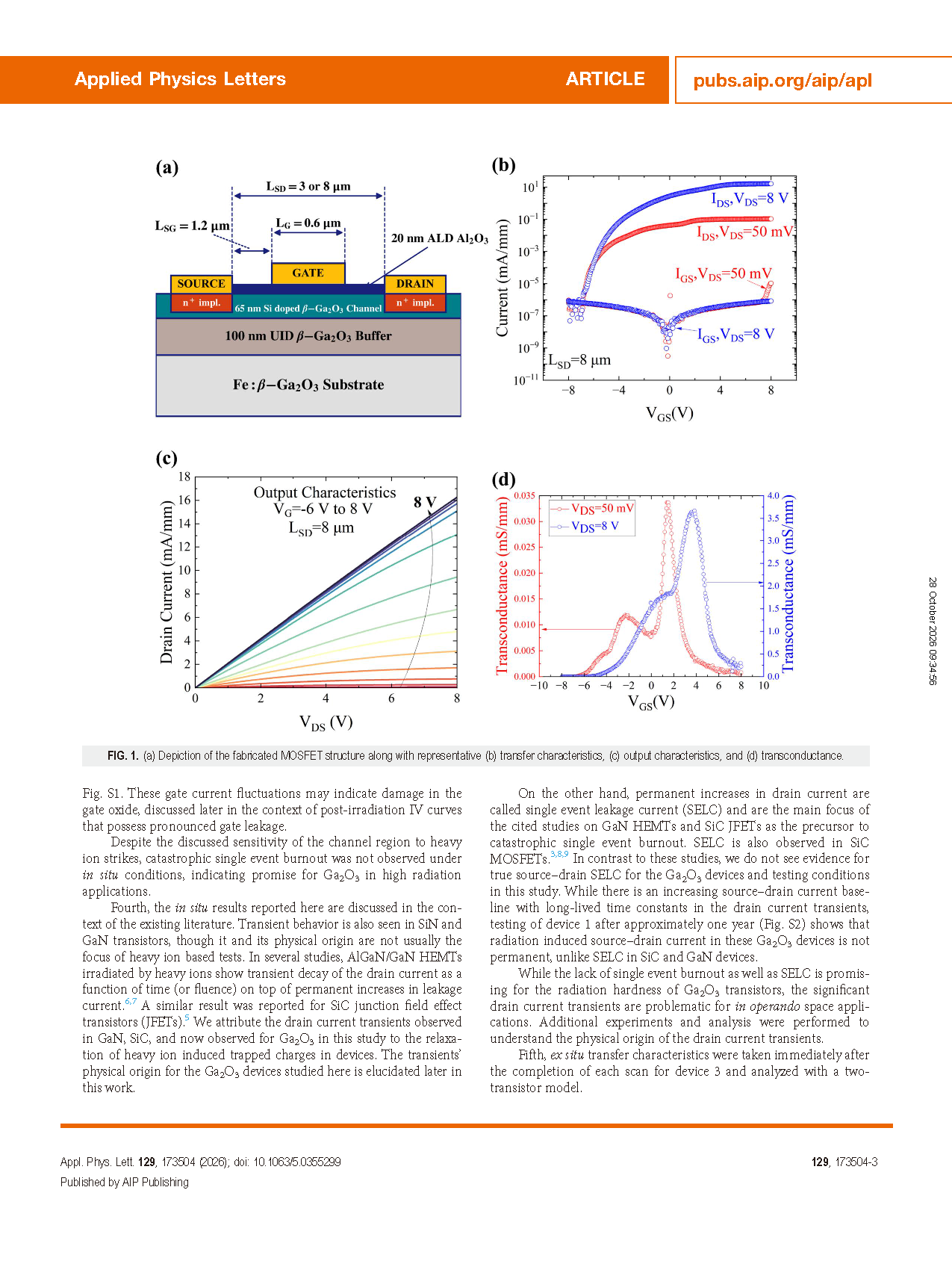
FIG. 1. (a) Depiction of the fabricated MOSFET structure along with representative (b) transfer characteristics, (c) output characteristics, and (d) transconductance.
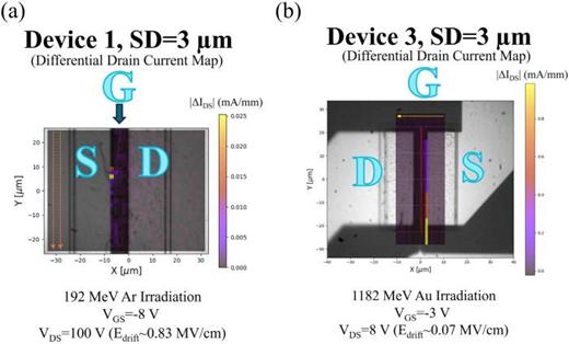
FIG. 2. Differential drain current mapping of (a) device 1 and (b) device 3 after scan 1. Arrows represent the rastering direction during heavy ion irradiation. The vertical red line in Fig. 2(b) indicates the gate finger.
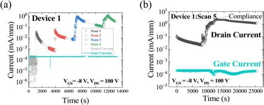
FIG. 3. Drain and gate current vs time for device 1 during (a) scans 1–4 and (b) scan 5.
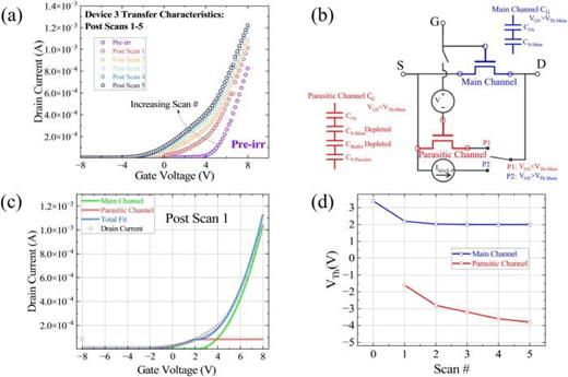
FIG. 4. (a) Transfer characteristics of device 3 pre-radiation and post each scan along with (b) a circuit diagram of the model used to fit the transfer data, (c) a fit of scan 1, and (d) extracted main channel and parasitic channel VTh as a function of scan #.
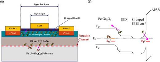
FIG. 5. (a) Real space depiction of the model that explains the transient behavior and threshold voltage shifts. (b) Energy band diagram, depicting emission of electrons from the main channel and parasitic channel through the substrate–buffer and oxide–channel interfaces which allows the drain current/negative threshold voltage shift to relax, as observed during in situ measurements. The band diagram is not drawn to scale—EF − EV is truncated to emphasize physically relevant energy barriers in the conduction band.
DOI:
doi.org/10.1063/5.0355299
Instruction
Official Account

Cooperation
Top
