


Researchers from Xidian University and China Resources Microelectronics have published a dissertation titled 6 A/1.6 kV or 1.4 GW/cm² β-Ga₂O₃ MOS-JFETs with Sandwiched-like RESURF Structure in IEEE Electron Device Letters.
Background
The ultra‑wide bandgap semiconductor β-Ga₂O₃ with large bandgap (Eg) of 4.8 eV and theoretical critical electric field of 8 MV/cm has been widely investigated and developed as the most promising materials for power electronics. Driven by the controllable n‑type doping and low‑cost availability of large‑diameter single‑crystal substrates, Ga₂O₃ devices have experienced rapid development from small to large‑periphery and exhibit strong market competitiveness. The potential of Ga₂O₃ material has been verified by 10‑kV diodes and transistors, high P‑FOM diodes exceeding 10 GW/cm² and JFETs up to 1 GW/cm², and RF transistors with record‑high fT×VDS of 1 THz·V and fmax = 90 GHz. As p‑type material incorporated to harness the potential of Ga₂O₃, 9 mm² Ga₂O₃ diode has been reported with a forward current (IF) up to 120 A and BV of 1.78 kV. Only very recently, the first Ga₂O₃ DC‑DC converter with large periphery of 94 mm has been demonstrated achieving an efficiency of over 90%. Moreover, 4 A / 300 V switching of Ga₂O₃ MOSFET was reported featuring a kilowatt‑class switching.
Abstract
In this work, high performance large‑ and small‑ periphery lateral β-Ga₂O₃ metal‑oxide‑semiconductor junction field‑effect‑transistors (MOS‑JFETs) were reported by employing sandwiched‑like reduced surface field (RESURF) technology. This RESURF structure was constructed with optimized p‑NiO at the gate region to deplete the channel and low permittivity (κ) SiO₂ to sustain higher electric field (E), while another p‑NiO above the SiO₂ layer helps to smooth the concentrated E. Therefore, our small‑ and large‑periphery devices with gate‑to‑drain spacing (LGD) of 8 μm deliver a high breakdown voltage (BV) of 3.24 and 1.63 kV, respectively, yielding a respective averaged E of 4 and 2 MV/cm. Attributed to the p‑NiO deployed between the gate and Ga₂O₃ channel, higher channel doping concentration (ND) was allowed while maintaining a good gate‑controlled turn‑off capability, which guaranteed the higher output current (ID) and lower specific on‑resistance (Ron,sp). The ID up to 6 A for large‑periphery MOS‑JFET with channel width (WCH) of 50 mm and a low Ron,sp of 7.5 mΩ·cm² for small‑periphery device with WCH of 20 μm are achieved, respectively. The Baliga’s power figure of merit (P‑FOM) of small‑ and large‑periphery MOS‑JFETs were calculated to be 1.4 and 0.26 GW/cm², which are one of the highest P‑FOMs among all small‑ and large‑periphery Ga₂O₃ FETs, illustrating the great potential of β-Ga₂O₃ MOS‑JFET with sandwiched‑like RESURF structure to high‑power switching operations.
Highlights
A novel sandwiched‑like charge‑balanced RESURF structure consisting of double p‑NiO layers sandwiching low‑κ SiO₂ is proposed.The bottom p‑NiO depletes the channel, the intermediate SiO₂ sustains high electric field, and the top p‑NiO mitigates electric‑field crowding, effectively alleviating the trade‑off between breakdown voltage and specific on‑resistance.
The RESURF technology is for the first time applied to large‑periphery β‑Ga₂O₃MOS‑JFET.A large‑size device with 50 mm channel width is fabricated, achieving a high output current of 6 A together with a kilovolt‑level breakdown voltage of 1.63 kV.
By inserting p‑NiO between the gate and Ga₂O₃channel, higher channel doping concentration is allowed while preserving satisfactory gate‑controlled turn‑off capability.The small‑periphery device achieves a breakdown voltage of 3.24 kV, a low specific on‑resistance of 7.5 mΩ·cm², and a state‑of‑the‑art power figure‑of‑merit of 1.4 GW/cm² among Ga₂O₃ FETs.
TCAD simulations reveal the suppression of electric‑field peak by the sandwiched‑like RESURF structure.Compared with the control device without RESURF from the same group, the breakdown voltage is boosted from 1.32 kV to 3.24 kV under similar gate‑drain spacing, which quantitatively verifies the enhancement of breakdown performance. Meanwhile, the feasibility of tunable p‑NiO material system is validated.
Conclusions
In summary, we have experimentally demonstrated the deployment of sandwiched‑like RESURF structure to lateral β‑Ga₂O₃ large‑ and small‑periphery MOS‑JFETs with the low‑κ SiO₂ inserted between two layers of the p‑NiO. The large‑periphery RESURF MOS‑JFET has achieved an ID of 6 A, a BV of 1.63 kV and a P‑FOM of 0.26 GW/cm², while the small‑periphery device has achieved an ID of 135 mA/mm, a BV of 3.24 kV and a record P‑FOM of 1.4GW/cm² among β‑Ga₂O₃ MOSFETs. These results indicate that the MOS‑JFETs with the charge‑balanced and sandwiched‑like RESURF architecture are promising technical solutions for advancing Ga₂O₃ device application.
Project Support
This work was supported by the National Natural Science Foundation of China (Grant No.62421005) and Guangdong Basic and Applied Basic Research Foundation (Grant No.2023B1515040024). This work is also supported by Fundamental and Interdisciplinary Disciplines Breakthrough Plan of the Ministry of Education of China with the Grant No. of JYB2025XDXM105.
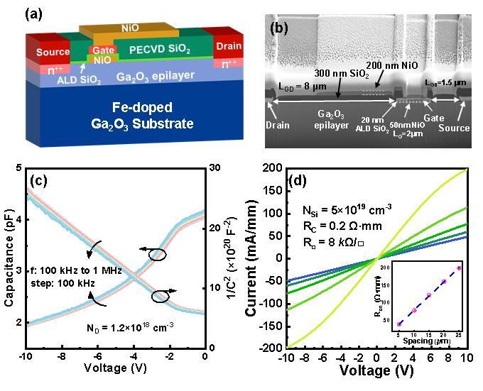
Fig.1 (a) 3-D schematic of the MOS-JFET with RESURF structure; (b) Cross-sectional SEM image of the device; (c) Frequency-dependent C-V and 1/C²-V characteristics of SiO₂/β-Ga₂O₃ MOS capacitor with small dispersion, the extracted epilayer doping ND=1.2×10¹⁸ cm⁻³; (d) I-V characteristics of TLM under NSi =5×10¹⁹ cm⁻³. Inset shows the fitting curve of on-resistance versus spacing, RC=0.2 Ω/mm and R□=8 kΩ/□ are extracted.
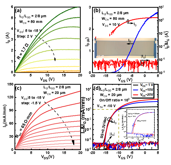
Fig.2 (a), (b) Pulsed output and transfer characteristics of large-periphery device with WCH=50 mm; (c), (d) DC output and transfer characteristics of small-periphery device with WCH=20 μm. The inset in (d) presents double-sweep transfer curves of small-periphery device with threshold hysteresis of 0.3 V.
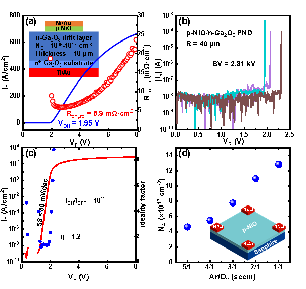
Fig.3 (a) Forward I-V characteristics and specific on-resistance of NiO/Ga₂O₃ PN diode, inset shows cross-sectional schematic; (b) Reverse characteristics of PN diode with low leakage current and 2.31 kV breakdown voltage without termination; (c) Log-scale IF-VF and η-VF characteristics of PN diode, the subthreshold swing is extracted; (d) Hole concentration of p-NiO measured by Van der Pauw Hall measurement as a function of Ar/O₂ ratio.
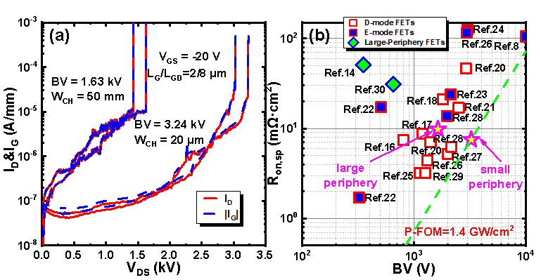
Fig.4 (a) Off-state characteristics of large- and small-periphery devices at VGS = -20 V and LGD =8 μm; (b) Benchmark of Ron,sp versus BV for state-of-the-art lateral β-Ga₂O₃ FETs.
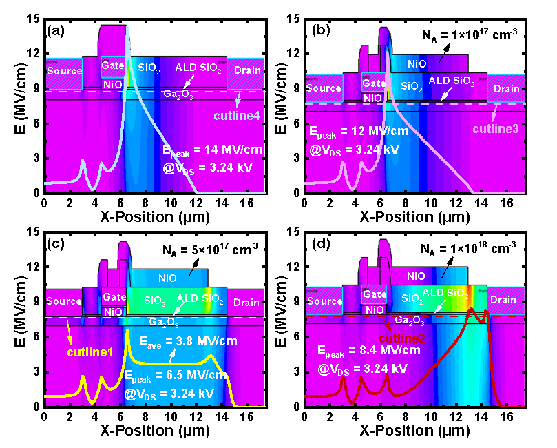
Fig.5 Simulated electric-field contour plots: (a) Ga₂O₃ MOS-JFET without RESURF; RESURF MOS-JFET with p-NiO acceptor concentration of (b) 1×10¹⁷ cm⁻³, (c) 5×10¹⁷ cm⁻³, (d) 1×10¹⁸ cm⁻³.
DOI:
10.1109/LED.2026.3740581
Instruction
Official Account

Cooperation
Top